EP1431988A1 - THIN FILM CAPACITY ELEMENT−USE COMPOSITION, HIGH−PERMITTIVITY INSULATION FILM, THIN FILM CAPACITY ELEMENT AND THIN FILM MULTILAYER CAPACITOR - Google Patents
THIN FILM CAPACITY ELEMENT−USE COMPOSITION, HIGH−PERMITTIVITY INSULATION FILM, THIN FILM CAPACITY ELEMENT AND THIN FILM MULTILAYER CAPACITOR Download PDFInfo
- Publication number
- EP1431988A1 EP1431988A1 EP02760744A EP02760744A EP1431988A1 EP 1431988 A1 EP1431988 A1 EP 1431988A1 EP 02760744 A EP02760744 A EP 02760744A EP 02760744 A EP02760744 A EP 02760744A EP 1431988 A1 EP1431988 A1 EP 1431988A1
- Authority
- EP
- European Patent Office
- Prior art keywords
- film
- thin
- dielectric
- capacitance device
- bismuth layer
- Prior art date
- Legal status (The legal status is an assumption and is not a legal conclusion. Google has not performed a legal analysis and makes no representation as to the accuracy of the status listed.)
- Withdrawn
Links
Images


Classifications
-
- H—ELECTRICITY
- H01—ELECTRIC ELEMENTS
- H01G—CAPACITORS; CAPACITORS, RECTIFIERS, DETECTORS, SWITCHING DEVICES, LIGHT-SENSITIVE OR TEMPERATURE-SENSITIVE DEVICES OF THE ELECTROLYTIC TYPE
- H01G4/00—Fixed capacitors; Processes of their manufacture
- H01G4/002—Details
- H01G4/018—Dielectrics
- H01G4/06—Solid dielectrics
- H01G4/08—Inorganic dielectrics
- H01G4/12—Ceramic dielectrics
-
- H—ELECTRICITY
- H10—SEMICONDUCTOR DEVICES; ELECTRIC SOLID-STATE DEVICES NOT OTHERWISE PROVIDED FOR
- H10P—GENERIC PROCESSES OR APPARATUS FOR THE MANUFACTURE OR TREATMENT OF DEVICES COVERED BY CLASS H10
- H10P14/00—Formation of materials, e.g. in the shape of layers or pillars
- H10P14/60—Formation of materials, e.g. in the shape of layers or pillars of insulating materials
- H10P14/69—Inorganic materials
- H10P14/692—Inorganic materials composed of oxides, glassy oxides or oxide-based glasses
- H10P14/6938—Inorganic materials composed of oxides, glassy oxides or oxide-based glasses the material containing at least one metal element, e.g. metal oxides, metal oxynitrides or metal oxycarbides
- H10P14/6939—Inorganic materials composed of oxides, glassy oxides or oxide-based glasses the material containing at least one metal element, e.g. metal oxides, metal oxynitrides or metal oxycarbides characterised by the metal
- H10P14/69397—Inorganic materials composed of oxides, glassy oxides or oxide-based glasses the material containing at least one metal element, e.g. metal oxides, metal oxynitrides or metal oxycarbides characterised by the metal the material containing two or more metal elements
-
- C—CHEMISTRY; METALLURGY
- C04—CEMENTS; CONCRETE; ARTIFICIAL STONE; CERAMICS; REFRACTORIES
- C04B—LIME, MAGNESIA; SLAG; CEMENTS; COMPOSITIONS THEREOF, e.g. MORTARS, CONCRETE OR LIKE BUILDING MATERIALS; ARTIFICIAL STONE; CERAMICS; REFRACTORIES; TREATMENT OF NATURAL STONE
- C04B35/00—Shaped ceramic products characterised by their composition; Ceramics compositions; Processing powders of inorganic compounds preparatory to the manufacturing of ceramic products
- C04B35/01—Shaped ceramic products characterised by their composition; Ceramics compositions; Processing powders of inorganic compounds preparatory to the manufacturing of ceramic products based on oxide ceramics
- C04B35/46—Shaped ceramic products characterised by their composition; Ceramics compositions; Processing powders of inorganic compounds preparatory to the manufacturing of ceramic products based on oxide ceramics based on titanium oxides or titanates
- C04B35/462—Shaped ceramic products characterised by their composition; Ceramics compositions; Processing powders of inorganic compounds preparatory to the manufacturing of ceramic products based on oxide ceramics based on titanium oxides or titanates based on titanates
- C04B35/475—Shaped ceramic products characterised by their composition; Ceramics compositions; Processing powders of inorganic compounds preparatory to the manufacturing of ceramic products based on oxide ceramics based on titanium oxides or titanates based on titanates based on bismuth titanates
-
- H—ELECTRICITY
- H01—ELECTRIC ELEMENTS
- H01G—CAPACITORS; CAPACITORS, RECTIFIERS, DETECTORS, SWITCHING DEVICES, LIGHT-SENSITIVE OR TEMPERATURE-SENSITIVE DEVICES OF THE ELECTROLYTIC TYPE
- H01G4/00—Fixed capacitors; Processes of their manufacture
- H01G4/002—Details
- H01G4/018—Dielectrics
- H01G4/06—Solid dielectrics
- H01G4/08—Inorganic dielectrics
- H01G4/10—Metal-oxide dielectrics
-
- H—ELECTRICITY
- H01—ELECTRIC ELEMENTS
- H01G—CAPACITORS; CAPACITORS, RECTIFIERS, DETECTORS, SWITCHING DEVICES, LIGHT-SENSITIVE OR TEMPERATURE-SENSITIVE DEVICES OF THE ELECTROLYTIC TYPE
- H01G4/00—Fixed capacitors; Processes of their manufacture
- H01G4/30—Stacked capacitors
-
- H—ELECTRICITY
- H10—SEMICONDUCTOR DEVICES; ELECTRIC SOLID-STATE DEVICES NOT OTHERWISE PROVIDED FOR
- H10D—INORGANIC ELECTRIC SEMICONDUCTOR DEVICES
- H10D84/00—Integrated devices formed in or on semiconductor substrates that comprise only semiconducting layers, e.g. on Si wafers or on GaAs-on-Si wafers
- H10D84/201—Integrated devices formed in or on semiconductor substrates that comprise only semiconducting layers, e.g. on Si wafers or on GaAs-on-Si wafers characterised by the integration of only components covered by H10D1/00 or H10D8/00, e.g. RLC circuits
- H10D84/204—Integrated devices formed in or on semiconductor substrates that comprise only semiconducting layers, e.g. on Si wafers or on GaAs-on-Si wafers characterised by the integration of only components covered by H10D1/00 or H10D8/00, e.g. RLC circuits of combinations of diodes or capacitors or resistors
- H10D84/212—Integrated devices formed in or on semiconductor substrates that comprise only semiconducting layers, e.g. on Si wafers or on GaAs-on-Si wafers characterised by the integration of only components covered by H10D1/00 or H10D8/00, e.g. RLC circuits of combinations of diodes or capacitors or resistors of only capacitors
-
- C—CHEMISTRY; METALLURGY
- C04—CEMENTS; CONCRETE; ARTIFICIAL STONE; CERAMICS; REFRACTORIES
- C04B—LIME, MAGNESIA; SLAG; CEMENTS; COMPOSITIONS THEREOF, e.g. MORTARS, CONCRETE OR LIKE BUILDING MATERIALS; ARTIFICIAL STONE; CERAMICS; REFRACTORIES; TREATMENT OF NATURAL STONE
- C04B2235/00—Aspects relating to ceramic starting mixtures or sintered ceramic products
- C04B2235/02—Composition of constituents of the starting material or of secondary phases of the final product
- C04B2235/30—Constituents and secondary phases not being of a fibrous nature
- C04B2235/32—Metal oxides, mixed metal oxides, or oxide-forming salts thereof, e.g. carbonates, nitrates, (oxy)hydroxides, chlorides
- C04B2235/3205—Alkaline earth oxides or oxide forming salts thereof, e.g. beryllium oxide
- C04B2235/3213—Strontium oxides or oxide-forming salts thereof
-
- C—CHEMISTRY; METALLURGY
- C04—CEMENTS; CONCRETE; ARTIFICIAL STONE; CERAMICS; REFRACTORIES
- C04B—LIME, MAGNESIA; SLAG; CEMENTS; COMPOSITIONS THEREOF, e.g. MORTARS, CONCRETE OR LIKE BUILDING MATERIALS; ARTIFICIAL STONE; CERAMICS; REFRACTORIES; TREATMENT OF NATURAL STONE
- C04B2235/00—Aspects relating to ceramic starting mixtures or sintered ceramic products
- C04B2235/02—Composition of constituents of the starting material or of secondary phases of the final product
- C04B2235/30—Constituents and secondary phases not being of a fibrous nature
- C04B2235/32—Metal oxides, mixed metal oxides, or oxide-forming salts thereof, e.g. carbonates, nitrates, (oxy)hydroxides, chlorides
- C04B2235/3231—Refractory metal oxides, their mixed metal oxides, or oxide-forming salts thereof
- C04B2235/3251—Niobium oxides, niobates, tantalum oxides, tantalates, or oxide-forming salts thereof
-
- C—CHEMISTRY; METALLURGY
- C04—CEMENTS; CONCRETE; ARTIFICIAL STONE; CERAMICS; REFRACTORIES
- C04B—LIME, MAGNESIA; SLAG; CEMENTS; COMPOSITIONS THEREOF, e.g. MORTARS, CONCRETE OR LIKE BUILDING MATERIALS; ARTIFICIAL STONE; CERAMICS; REFRACTORIES; TREATMENT OF NATURAL STONE
- C04B2235/00—Aspects relating to ceramic starting mixtures or sintered ceramic products
- C04B2235/70—Aspects relating to sintered or melt-casted ceramic products
- C04B2235/74—Physical characteristics
- C04B2235/78—Grain sizes and shapes, product microstructures, e.g. acicular grains, equiaxed grains, platelet-structures
- C04B2235/787—Oriented grains
-
- C—CHEMISTRY; METALLURGY
- C04—CEMENTS; CONCRETE; ARTIFICIAL STONE; CERAMICS; REFRACTORIES
- C04B—LIME, MAGNESIA; SLAG; CEMENTS; COMPOSITIONS THEREOF, e.g. MORTARS, CONCRETE OR LIKE BUILDING MATERIALS; ARTIFICIAL STONE; CERAMICS; REFRACTORIES; TREATMENT OF NATURAL STONE
- C04B2235/00—Aspects relating to ceramic starting mixtures or sintered ceramic products
- C04B2235/70—Aspects relating to sintered or melt-casted ceramic products
- C04B2235/96—Properties of ceramic products, e.g. mechanical properties such as strength, toughness, wear resistance
- C04B2235/963—Surface properties, e.g. surface roughness
-
- H—ELECTRICITY
- H10—SEMICONDUCTOR DEVICES; ELECTRIC SOLID-STATE DEVICES NOT OTHERWISE PROVIDED FOR
- H10D—INORGANIC ELECTRIC SEMICONDUCTOR DEVICES
- H10D1/00—Resistors, capacitors or inductors
- H10D1/60—Capacitors
- H10D1/68—Capacitors having no potential barriers
- H10D1/682—Capacitors having no potential barriers having dielectrics comprising perovskite structures
-
- H—ELECTRICITY
- H10—SEMICONDUCTOR DEVICES; ELECTRIC SOLID-STATE DEVICES NOT OTHERWISE PROVIDED FOR
- H10P—GENERIC PROCESSES OR APPARATUS FOR THE MANUFACTURE OR TREATMENT OF DEVICES COVERED BY CLASS H10
- H10P14/00—Formation of materials, e.g. in the shape of layers or pillars
- H10P14/60—Formation of materials, e.g. in the shape of layers or pillars of insulating materials
- H10P14/63—Formation of materials, e.g. in the shape of layers or pillars of insulating materials characterised by the formation processes
- H10P14/6326—Deposition processes
- H10P14/6328—Deposition from the gas or vapour phase
- H10P14/6329—Deposition from the gas or vapour phase using physical ablation of a target, e.g. physical vapour deposition or pulsed laser deposition
Definitions
- the present invention relates to compositions for thin-film capacitance device, high-dielectric constant insulating film, thin-film capacitance device, and thin-film multilayer capacitor. More particularly, the invention relates to compositions for thin-film capacitance device used as dielectric thin-films or so for thin-film capacitance device of every kind, such as condenser or capacitor having conductor-insulator-conductor structure and thin-film capacitance device such as condenser or capacitor wherein said compositions for thin-film capacitance device is used as dielectric thin-film.
- thin-film capacitor using a layer dielectric thin-film in respect of integrated circuit with active component such as transistor, is delayed for more compact body. This is a factor of obstruction for realizing ultrahigh integrated circuit. More compact body for thin-film capacitor is delayed because dielectric constant of dielectric materials used for the thin-film capacitor was low. Accordingly, in order to realize more compact body and relatively high capacitance, the use of dielectric materials with high dielectric constant is important.
- each layer for dielectric layer is desired to be further thinner as much as possible(further thinner layer) and the number of laminated layers for dielectric layer at a fixed size is desired to improve as much as possible(multiple layers).
- sheet method(A method comprising the following steps.
- Dielectric green sheet layer is formed such as by doctor blade method on carrier film using dielectric layer paste.
- internal electrode paste is printed by fixed pattern. Afterwards, these are peeled off and laminated by each layer.
- the dielectric layer was difficult to be further thinner, for instance, 2 ⁇ m or less.
- the number of laminated layers had its limit.
- printing method(A method, using screen printing method or so which plural number of dielectric layer paste and internal electrode paste are alternately printed on carrier film and then the carrier film is peeled off.
- dielectric thin-film formed by the methods described in these publications have bad surface smoothing property and when too many of the dielectric thin-film are layered, electrode may short-circuit in some cases. Accordingly, the number of laminated layers of at most 12 to 13 or so can only be produced, so that even capacitor was capable of realizing more compact body, it was not capable of higher capacitance.
- composition composes a bulk bismuth layer-structured compound dielectric obtained by sintering method; a composition expressed by formula: (Bi 2 O 2 ) 2+ (A m-1 B m O 3m+1 ) 2- or Bi 2 A m-1 B m O 3m+3 wherein symbol m is selected from positive numbers of 1 to 8, symbol A is at least one element selected from Na, K, Pb, Ba, Sr, Ca and Bi and B is at least one element selected from Fe, Co, Cr, Ga, Ti, Nb, Ta Sb, V, Mo and W.
- this article did not describe under which condition(ex. the relation between substrate surface and degree of c-axis orientation) the compositions shown by abovementioned formula are made further thinner(ex. 1 ⁇ m or less) in order to obtain the following thin-film.
- a thin-film which is, when made further thinner, capable of providing relatively high dielectric constant and low loss, and also superior leak property, break-down voltage, temperature characteristic of dielectric constant and surface smoothness property.
- the object of the invention is to provide compositions for thin-film capacitance device that are, even made further thinner, capable of providing relatively high dielectric constant and low-loss, and also superior leak property, break-down voltage, temperature characteristic of dielectric constant and surface smoothness property, and to provide thin-film capacitance device using the compositions.
- another object of the present invention is, by using these thin-film capacitance device compositions as dielectric thin-film, to provide a thin-film multilayer capacitor which can give more compact body and relatively high capacitance.
- the present invention is also to provide high-dielectric constant insulating film which provide, even made further thinner, relatively high dielectric constant and low-loss, also superior leak property, break-down voltage, temperature characteristic of dielectric constant and surface smoothness property.
- the inventors of the present invention have earnestly considered of dielectric thin-film materials used for capacitor and its crystal structure.
- a bismuth layer-structured compound having specific composition moreover, by orientating c-axis([001]orientation) of the bismuth layer-structured compound vertically to substrate surface and composing dielectric thin-film as thin-film capacitance device compositions, that is, by forming c-axis orientation film(thin-film normal is parallel to c-axis) of bismuth layer-structured compound on to the substrate surface, it was found that thin-film capacitance device compositions and thin-film capacitance device using the compositions could be provided.
- the thin-film capacitance device compositions are, even made further thinner, relatively high dielectric constant and low-loss(low tan ⁇ ) can be provided, and also superior leak property, break-down voltage, temperature characteristic of dielectric constant and surface smoothness property.
- these thin-film capacitance device compositions as dielectric thin-film, it was found that number of laminated layers can be increased and thin-film multilayer capacitor which can give more compact body and relatively high capacitance can be provided. This brought completion of the present invention.
- these compositions as high dielectric constant insulating film, it was found that the compositions can be applied other than as thin-film capacitance device, which brought completion of the present invention.
- thin-film capacitance device compositions including a bismuth layer-structured compound whose c-axis is oriented vertically to a substrate surface wherein said bismuth layer-structured compound is expressed by a formula: (Bi 2 O 2 ) 2+ (A m-1 B m O 3m+1 ) 2- or Bi 2 A m-1 B m O 3m+3 in which symbol "m” is selected from odd numbers, symbol "A” is at least one element selected from Na, K, Pb, Ba, Sr, Ca and Bi and symbol “B” is at least one element selected from Fe, Co, Cr, Ga, Ti, Nb, Ta Sb, V, Mo and W.
- Thin-film is a film for materials whose thickness is about several ⁇ to several ⁇ m and formed by thin-film forming method of every kind.
- Thin-film excludes a thick-film bulk whose thickness is about several hundreds ⁇ m or more and formed by sintering method.
- Thin-film includes continuous film which covers fixed area continuously and also intermittent film which covers optional intervals intermittently.
- Thin-film may be formed at a part of substrate surface and may also be formed at the entire surface.
- the thickness of dielectric thin-film(or high dielectric constant insulating film) formed by thin-film capacitance device compositions according to the invention is preferably 5 to 1000nm. When at this thickness, the present invention is quite effective.
- the process of manufacturing thin-film capacitance device compositions according to the invention is not particularly limited but it can be manufactured by, for instance, using substrates of cubic system, tetragonal system, orthorhombic system, or monoclinic system that are [100] oriented, and forming thin-film capacitance device compositions including a bismuth layer-structured compound which is expressed by a formula: (Bi 2 O 2 ) 2+ (A m-1 B m O 3m+1 ) 2- or Bi 2 A m-1 B m O 3m+3 wherein symbol "m” is selected from odd numbers, symbol "A” is at least one element selected from Na, K, Pb, Ba, Sr, Ca and Bi and symbol "B” is at least one element selected from Fe, Co, Cr, Ga, Ti, Nb, Ta Sb, V, Mo and W.
- the abovementioned substrate is preferably composed by single crystal.
- Thin-film capacitance device of the invention is characterized in a thin-film capacitance device wherein lower electrode, dielectric thin-film and upper electrode are formed one by one on the substrate and said dielectric thin-film is composed of abovementioned thin-film capacitance device compositions of the invention.
- Thin-film multilayer capacitor of the invention comprising dielectric thin-films and internal electrode thin-films alternately layered on a substrate, wherein said dielectric thin-films are composed of abovementioned thin-film capacitance device compositions of the invention.
- a bismuth layer-structured compound whose c-axis is oriented 100% vertically to the substrate surface that is, a bismuth layer-structured compound whose degree of c-axis orientation is 100%, which is particularly preferable.
- the degree of c-axis orientation may not be complete 100%.
- said bismuth layer-structured compound whose degree of c-axis orientation is 80% or more, more preferably, 90% or more, most preferably, 95% or more.
- degree of c-axis orientation is 80% or more, more preferably, 90% or more, most preferably, 95% or more.
- "m” in the formula composing said bismuth layer-structured compound is 1, 3, 5 or 7, more preferably, 1, 3 or 5. This is due to the easiness of manufacturing.
- said thin-film capacitance device compositions further include rare-earth element(at least one element selected from Sc, Y, La, Ce, Pr, Nd, Pm, Sm, Eu, Gd, Tb, Dy, Ho, Er, Tm, Yb and Lu).
- rare-earth element at least one element selected from Sc, Y, La, Ce, Pr, Nd, Pm, Sm, Eu, Gd, Tb, Dy, Ho, Er, Tm, Yb and Lu.
- said rare-earth element is "Re" and when said bismuth layer-structured compound is expressed by formula: Bi 2 A m-1-x Re x B m O 3m+3 , said x is 0.4 to 1.8, more preferably, 1.0 to 1.4.
- Including rare-earth element decreases leak current and short ratio, and also Curie temperature can be -100°C or more to 100°C or less:
- said thin-film capacitance device compositions have Curie temperature of -100°C or more to 100°C or less.
- said internal electrode thin-film is composed of noble metal, base metal or conductive oxide.
- said substrate may be composed of amorphous material.
- Lower electrode(or internal electrode thin-film) formed on the substrate is preferably [100] oriented. By forming lower electrode to [100] orientation, c-axis of a bismuth layer-structured compound composing dielectric thin-film formed on the lower electrode can orient vertically to the substrate surface.
- Thin-film capacitance device compositions of the invention and dielectric thin-film as their example are composed of c-axis oriented bismuth layer-structured compound having specific composition.
- Thin-film capacitance device compositions composed of c-axis oriented bismuth layer-structured compound having specific composition are, even when film thickness is made further thinner, relatively high dielectric constant(ex. more than 200) and low loss(tan ⁇ is 0.02 or less) can be provided. They can also provide superior leak property(ex. leak current is 1 ⁇ 10 -7 A/cm 2 or less and short ratio is 10% or less when measured at 50kV/cm electrolytic strength), improved break-down voltage(ex. 1000kV/cm or more), superior temperature characteristic of dielectric constant(ex. average change rates of dielectric constant to temperature is within ⁇ 500ppm/ °C at reference temperature of 25°C) and superior surface smoothness property(ex. surface roughness: Ra is 2nm or less).
- thin-film capacitance device compositions according to the present invention are, when its film thickness is made further thinner, relatively high dielectric constant can be provided. Moreover, due to the satisfactory surface smoothness, increasing number of laminated layers for dielectric thin-film as said thin-film capacitance device compositions is capable. Therefore, by using the thin-film capacitance device compositions, thin-film multilayer capacitor that can give more compact body and relatively high capacitance can be provided.
- thin-film capacitance device compositions and thin-film capacitance device of the invention are superior in frequency characteristic(ex. At specific temperature, ratio of dielectric constant value at high frequency domain of 1MHz and those at lower than the above frequency domain of 1kHz is 0.9 to 1.1 in absolute value.) and also in voltage characteristic (ex. At specific frequency, ratio of dielectric constant value at measuring voltage of 0.1V and those at measuring voltage of 5V is 0.9 to 1.1 in absolute value).
- thin-film capacitance device compositions of the invention are superior in temperature characteristic for electrostatic capacity(average change rates of the electrostatic capacity to temperature is within ⁇ 500ppm/°C at reference temperature of 25°C).
- conductor -insulator-conductor structured condenser (ex. single layer typed thin-film capacitor or multilayer typed thin-film multilayer capacitor) or capacitor(ex. such as for DRAM) are exemplified.
- dielectric thin-film compositions for condenser or dielectric thin-film compositions for capacitor are exemplified.
- High dielectric constant insulating film of the invention is composed of the same compositions as thin-film capacitance device compositions of the invention.
- High dielectric constant insulating film of the invention can be used as, other than thin-film dielectric film for thin-film capacitance device or capacitor, gate-insulating film of semiconductor device or intermediate insulating film between gate electrode and floating gate or so.
- thin-film capacitor 2 includes substrate 4, and on the substrate 4, lower electrode thin-film 6 is formed. On lower electrode thin-film 6, dielectric thin-film 8 is formed. On dielectric thin-film 8, upper electrode thin-film 10 is formed.
- Substrate 4 is composed of single crystal with high matched lattice (ex. single crystal of SrTiO 3 , MgO or LaAl O 3 ), amorphous materials(ex. glass, fused quartz or SiO 2 /Si) and other materials(ex ZrO 2 /Si or CeO 2 /Si) or so. Particularly, composed of substrate oriented to such as [100] orientation e.g. cubic system, tetragonal system, orthorhombic system, or monoclinic system, are preferable. Thickness of substrate 4 is not particularly limited but is about 100 to 1000 ⁇ m.
- lower electrode thin-film 6 is preferably composed of conductive oxide, such as CaRuO 3 or SrRuO 3 , or noble metal such as Pt or Ru, more preferably, [100] oriented conductive oxide or noble metal.
- conductive oxide or noble metal which is [100] oriented can be formed on its surface.
- temperature of substrate 4 for forming lower electrode thin-film 6 on its surface is preferably 300°C or more, more preferably 500°C or more.
- Lower electrode thin-film 6 using amorphous materials for substrate 4 can be composed of conductive glass such as ITO.
- conductive glass such as ITO.
- [100] oriented lower electrode thin-film 6 can easily be formed on the surface. Due to this, degree of c-axis orientation of dielectric thin-film 8 formed on the lower electrode thin-film 6 tends to increase.
- amorphous materials such as glass for substrate 4
- noble metal such as gold(Au), palladium(Pd), Silver(Ag) or their alloys and also base metal such as Nickel(Ni), Copper(Cu) or their alloys can be used.
- the thickness of lower electrode thin-film 6 is not limited but preferably 10 to 1000nm, more preferably 50 to 100nm or so.
- Upper electrode thin-film 10 can be composed of the same material as said lower electrode thin-film 6. And the thickness can also be the same.
- Dielectric thin-film 8 is an example of thin-film capacitance device compositions of the invention, and include bismuth layer-structured compound expressed by formula: (Bi 2 O 2 ) 2+ (A m-1 B m O 3m+1 ) 2- or Bi 2 A m-1 B m O 3m+3.
- bismuth layer-structured compound shows a laminar structure which upper and lower parts of laminar perovskite layer, which perovskite lattice composed of (m-1) numbers of ABO 3 is ranged, are sandwiched by a pair of Bi and O layer.
- the bismuth layer-structured compound improves its degree of orientation to [001] orientation, that is, degree of c-axis orientation .
- c-axis of bismuth layer-structured compound is vertically oriented to substrate 4 to form dielectric thin-film 8.
- the degree of c-axis orientation for the bismuth layer-structured compound is 100%, however, the degree of c-axis orientation may not be complete 100%.
- the degree of c-axis orientation may be c-axis oriented.
- the degree of c-axis orientation of the bismuth layer-structured compound may be preferably 80% or more.
- the degree of c-axis orientation of the bismuth layer-structured compound may be preferably 90% or more, more preferably, 95% or more.
- P is ( ⁇ ⁇ I(001)/ ⁇ I(hkl) ⁇ ) showing the ratio of the sum ⁇ I(001) of reflecting strength I(001) from (001) surface to the sum ⁇ I(hkl) of reflecting strength I(hkl) from each crystal surface(hkl) and P0 is the same.
- c-axis of the bismuth layer-structured compound signifies an orientation which a pair of (Bi 2 O 2 ) 2+ layers are connected to, that is, [001] orientation.
- dielectric characteristic of dielectric thin-film 8 give its full ability. That is, even making thickness of dielectric thin-film 8 further thinner, such as 100nm or less, relatively high dielectric constant and low-loss(tan ⁇ is low) can be provided. And it also provides superior leak property, improved break-down voltage, superior temperature characteristic of dielectric constant and superior surface smoothness property. When tan ⁇ decreases, loss Q(1/tan ⁇ ) value increases.
- the symbol “A” is composed of at least one element selected from Na, K, Pb, Ba, Sr, Ca and Bi. Further, when the symbol “A” is composed of two or more elements, the ratio of those elements is optional.
- the symbol “B” is composed of at least one element selected from Fe, Co, Cr, Ga, Ti, Nb, Ta, Sb, V, Mo and W. Further, when the symbol “B” is composed of two or more elements, the ratio of those elements is optional.
- Dielectric thin-film 8 to said bismuth layer-structured compound, further include at least one element(rare-earth element: Re) selected from Sc, Y, La, Ce, Pr, Nd, Pm, Sm, Eu, Gd, Tb, Dy, Ho, Er, Tm, Yb and Lu is preferable.
- Curie temperature(temperature of phase transition from ferroelectric to paraelectric) of dielectric thin-film 8 can be kept, preferably, -100°C or more to 100°C or less, more preferably -50°C or more to 50°C or less.
- Curie point is -100°C to +100°C
- dielectric constant of dielectric thin-film 8 increases.
- Curie temperature can be measured by DSC(differential scanning calorimetry) or so. Further, when Curie point is less than ambient temperature(25°C), tan ⁇ further decreases and consequently, the loss Q value further increases.
- dielectric thin-film 8 even without rare-earth element Re, is superior in leak characteristic as following. However, with substitution of Re, leak characteristic can be further superior.
- leak current measured when 50kV/cm field intensity can be preferably 1 ⁇ 10 -7 A/cm 2 or less, more preferably 5 ⁇ 10 -8 A/cm 2 or less, further, short ratio can be preferably 10% or less, more preferably, 5% or less.
- leak current measured under the same condition can be preferably 5 ⁇ 10 -8 A/cm 2 or less, more preferably 1 ⁇ 10 -8 A/cm 2 or less, further, short ratio can be preferably 5% or less, more preferably, 3% or less.
- Dielectric thin-film 8 has preferably film thickness of 200nm or less and considering higher capacitance, more preferably those of 100nm or less. Further, the minimum of film thickness, considering insulating character of film, is preferably about 30nm.
- surface roughness(Ra) based upon JIS ⁇ B0601 is preferably 2nm or less, more preferably 1 nm or less.
- dielectric constant at 25°C(ambient temperature) and 100kHz(AC20mV) metering frequency is preferably more than 200, more preferably 250 or more.
- tan ⁇ at 25 °C (ambient temperature) and 100kHz(AC20mV) metering frequency is preferably 0.02 or less, more preferably 0.01 or less. Further, the loss Q value is preferably 50 or more, more preferably 100 or more.
- dielectric constant change(particularly a decline) is small.
- ratio of dielectric constant value at high frequency domain of 1MHz and those at lower than above frequency domain of 1kHz can be 0.9 to 1.1 in absolute value. Namely, frequency characteristic is satisfactory.
- dielectric thin-film 8 even when metering voltage(impressed voltage) at specific frequency(ex. 10kHz, 100 kHz or 1MHz) is changed to about 5V or so, dielectric constant change is small.
- ratio of dielectric constant value at metering voltage of 0.1V and those at metering voltage of 5V can be 0.9 to 1.1. Namely, voltage characteristic is satisfactory.
- Such dielectric thin-film 8 can be formed by thin-film forming method of every kind such as vacuum evaporation method, high frequency sputtering method, pulsed laser deposition method(PLD), MOCVD(Metal Organic Chemical Vapor Deposition)method or sol-gel method.
- thin-film forming method of every kind such as vacuum evaporation method, high frequency sputtering method, pulsed laser deposition method(PLD), MOCVD(Metal Organic Chemical Vapor Deposition)method or sol-gel method.
- dielectric thin-film 8 is formed.
- substrate 4 composed of amorphous material is more preferable.
- dielectric thin-film 8 a bismuth layer-structured compound having specific composition is composed by orientating to c-axis.
- Dielectric thin-film 8 and thin-film capacitor 2 using the dielectric thin-film 8 are, even film thickness of dielectric thin-film is made thinner, such as 100nm or less, relatively high dielectric constant and low loss can be provided. They can also provide superior leak property, improved break-down voltage, superior temperature characteristic of dielectric constant and superior surface smoothness property.
- dielectric thin-film 8 and thin-film capacitor 2 are also superior in frequency characteristic or voltage characteristic.
- the present embodiment is described by exemplifying, as thin-film capacitance device, a thin-film multilayer capacitor forming multilayer dielectric thin-film.
- thin-film multilayer capacitor 20 includes capacitor body 22.
- the capacitor body 22 has multilayer structure which on the substrate 4a, a multiple number of dielectric thin-film 8a and internal electrode thin-film 24 and 26 are alternately arranged and protection film 30 is formed to cover dielectric thin-film 8a arranged at the most external part.
- a pair of external electrodes 28 and 29 is formed.
- the pair of external electrodes 28 and 29 is electrically connected to each of the exposed edge faces of a multiple number of internal electrode thin-film 24 and 26 that are alternately arranged inside capacitor body 22 to form capacitor circuit.
- the shape of capacitor body 22 is not particularly limited but normally, rectangular parallelepiped. Further, its size is not limited but for instance, it has about length of (0.01 to 10 mm) ⁇ width of (0.01 to 10 mm) ⁇ height of (0.01 to 1 mm).
- Substrate 4a is composed of the same material as substrate 4 in abovementioned first embodiment.
- Dielectric thin-film 8a is composed of the same material as dielectric thin-film 8 in abovementioned first embodiment.
- Internal electrode thin-films 24 and 26 are composed of the same material as lower electrode thin-film 6 and upper electrode thin-film 10 in abovementioned first embodiment.
- Material of external electrode 28 and 29 is not limited and the external electrode is composed of conductive oxide such as CaRuO 3 or SrRuO 3 ; base metal such as Cu, Cu alloys, Ni or Ni alloys; noble metal such as Pt, Ag, Pd or Ag-Pd alloys.
- the thickness is not limited but for instance, 10 to 1000nm or so.
- Material of protection film 30 is not limited but composed of such as silicon oxide film or aluminum oxide film.
- Thin-film multilayer capacitor 20 have first layer of internal electrode thin-film 24 formed on substrate 4a by masking with metal mask or so, then, dielectric thin-film 8a formed on the internal electrode thin-film 24 and further, second layer of internal electrode thin-film 26 formed on the dielectric thin-film 8a. After these processes are repeated for multiple times, dielectric thin-film 8a arranged at the most external part and opposite side of the substrate 4a is covered with protection film 30. And on the substrate 4a, a multiple number of internal electrode thin-film 24 and 26 and dielectric thin-film 8a alternately arranged capacitor body 22 is formed. Covering the protection film 30 can decrease the effect of moisture in atmosphere on internal part of capacitor body 22.
- substrate 4a composed of amorphous material is more preferable.
- Dielectric thin-film 8a of the present embodiment is, even when made thinner, relatively high dielectric constant can be provided and moreover, surface smoothness property is satisfactory. Due to these, the number of laminated layers can be 20 or more, preferably 50 or more. Accordingly, thin-film multilayer capacitor 20 which may be small-sized and relatively high capacitance can be provided.
- average change rates( ⁇ ) of dielectric constant is preferably within ⁇ 500ppm/ °C (25 °C reference temperature), and more preferably within ⁇ 250ppm/°C.
- Dielectric constant(no unit) was calculated from electrostatic capacity, electrode dimension and interelectrode distance of capacitor sample.
- the electrostatic capacity was measured by using digital LCR meter(4274A, YHP made) at capacitor sample, at ambient temperature(25 °C) and 100kHz(AC20mV) metering frequency.
- Tan ⁇ was measured under the same condition as above electrostatic capacity was measured and the loss Q value was also calculated.
- Leak current characteristic(Unit is A/cm 2 ) was measured at 50kV/cm field intensity.
- Short ratio(Unit is %) was determined by measuring 20 upper electrodes and calculating the ratio of which short-circuit among them.
- c-axis orientation film for bismuth' layer-structured compound of example 1 is inferior in dielectric constant, but superior in leak characteristic. Accordingly, not only even thinner-film can be expected but higher capacitance for thin-film capacitor can be expected. Moreover, at example 1, it was confirmed that in comparison to the other orientation directions of comparative examples land 2, its temperature characteristic was superior. Further, it was also confirmed that since Example 1 was superior in surface smoothness property in comparison to comparative examples land 2, it can be preferable thin-film material for manufacturing multilayer structure. Namely, according to example1, validity of c-axis orientation film for bismuth layer-structured compound was confirmed.
- the result is shown that as the film thickness of PZT thin-film was made thinner to 500nm, 200nm and 80nm, the dielectric constant(@1kHz) decreased to 300, 250 and 100 respectively.
- Reference 2 (Y. Takeshima, K. Tanaka and Y. Sakabe, Jpn. J. Appl. Phys.
- Curie point(Unit is °C) of dielectric thin-film is obtained by temperature change of dielectric constant.
- Composition (x ) Curie Point (°C) Dielectric Constant tan ⁇
- composition "x" for c-axis orientation film of SBTT increased, Curie point decreased and dielectric constant at ambient temperature(25°C) increased.
- composition "x" was about 1
- Curie point was around ambient temperature, and dielectric constant at ambient temperature was at maximum.
- composition "x” was about 1 or more, it became paraelectric phase at ambient temperature that the loss Q value increased. Namely, it was confirmed that, when high capacitance was required, composition range of 1.0 ⁇ x ⁇ 1.2 was suitable.
- composition range of 1.0 ⁇ x ⁇ 1.4 was suitable.
- SrTiO 3 single crystal substrate(thickness of 0.3mm) 4a (See Fig. 2, the same for following), which was [100] oriented, was prepared. And on the substrate 4a, by masking with metal mask of given pattern, with pulsed laser deposition method, 100nm film thickness of CaRuO 3 made electrode thin-film as internal electrode thin-film 24 was formed(pattern 1).
- SBTT thin-film as dielectric thin-film 8a was formed in the same way as example 1, except film thickness was 100nm.
- XRD X-ray diffraction
- SBTT thin-film as dielectric thin-film 8a was formed again in the same way as example 1, except film thickness was 100nm.
- a pair of external electrodes 28 and 29 composed of Ag is formed to obtain rectangular parallelepiped configuration of thin-film multilayer capacitor sample having length of 1mm ⁇ width of 0.5mm ⁇ thickness of 0.4mm.
- Electric characteristic(dielectric constant, dielectric loss, Q value, leak current and short ratio) of obtained capacitor sample were evaluated in the same way as example 1. The results were 250 dielectric constant, 0.01 tan ⁇ , 100 loss Q value and 1 ⁇ 10 -7 A/cm 2 leak current and were satisfactory. Further, temperature characteristic of dielectric constant for capacitor sample was evaluated in the same way as example 1 and its temperature coefficient was 190ppm/°C.
- composition range of 0.4 ⁇ x ⁇ 1.4 was suitable.
- thin-film capacitor sample manufactured at example 1 frequency characteristic and voltage characteristic were evaluated.
- Frequency characteristic was evaluated as following. At the capacitor sample, by changing frequency from 1kHz to 1MHz at ambient temperature(25°C), electrostatic capacity was measured and also dielectric constant was calculated. The results are shown in Figure 3. For the measurement of electrostatic capacity, LCR meter was used. As shown in Fig.3, even changing frequency to 1MHz at specific temperature, it was confirmed that dielectric constant value does not change. Namely, it was confirmed that frequency characteristic is superior.
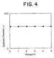
- Voltage characteristic was evaluated as following. At the capacitor sample, by changing metering voltage(impressed voltage) at specific frequency(100 kHz) from 0.1V(50kV/cm electrolytic strength) to 5V(250kV/cm electrolytic strength), electrostatic capacity was measured(Metering temperature was 25°C) at specific voltage and also dielectric constant was calculated. The results are shown in Figure 4. For the measurement of electrostatic capacity, LCR meter was used. As shown in Figure 4, even changing metering voltage to 5V at specific frequency, it was confirmed that dielectric constant value does not change. Namely, it was confirmed that voltage characteristic is superior.
- high dielectric constant insulating film of the invention is suitable for a gate insulating film.
Landscapes
- Engineering & Computer Science (AREA)
- Power Engineering (AREA)
- Chemical & Material Sciences (AREA)
- Manufacturing & Machinery (AREA)
- Ceramic Engineering (AREA)
- Microelectronics & Electronic Packaging (AREA)
- Inorganic Chemistry (AREA)
- Materials Engineering (AREA)
- Structural Engineering (AREA)
- Organic Chemistry (AREA)
- Fixed Capacitors And Capacitor Manufacturing Machines (AREA)
- Inorganic Insulating Materials (AREA)
- Ceramic Capacitors (AREA)
Abstract
Description
| Substrate Surface Orientation | Film Orientation | Surface Roughness Ra (nm) | Leak Current (A/cm2) | Short Ratio (%) | |
| Ex. 1 | [100] | [001] | 0.5 | 1×10⁻⁸ | 5 |
| Comp. Ex.1 | [110] | [118] | 3 | 5×10⁻⁷ | 40 |
| Comp. Ex.2 | [111] | [104] | 15 | 5×10⁻⁵ | 80 |
| Dielectric Constant | Temperature Coefficient (ppm/°C) | tan δ | The Loss Q Value | |
| Ex. 1 | 250 | <±200 | <0.01 | >100 |
| Comp. Ex.1 | 350 | ±1000 | >0.01 | <100 |
| Comp. Ex.2 | 350 | ±1000 | >0.01 | <100 |
| Film Thickness (nm) | Surface Roughness Ra(nm) | Leak Current (A/cm2) | Break-down Voltage (kV/cm) | Dielectric Constant | |
| Ex. 2 | 35 | 0.5 | 4×10⁻⁷ | >1000 | 250 |
| Ex. 3 | 50 | 0.5 | 1×10⁻⁷ | >1000 | 250 |
| Ex. 4 | 100 | 0.5 | 3×10⁻⁸ | >1000 | 250 |
| Temperature Coefficient(ppm/°C) | tan δ | The Loss Q Value | |
| Ex. 2 | <±200 | <0.04 | >25 |
| Ex. 3 | <±200 | <0.02 | >50 |
| Ex. 4 | <±200 | <0.01 | >100 |
| Composition (x=) | Curie Point (°C) | Dielectric Constant | tan δ | The Loss Q Value | |
| Ex. 5 | 0.4 | 500 | 150 | <0.02 | >50 |
| Ex. 5 | 0.6 | 350 | 170 | <0.025 | >40 |
| Ex. 5 | 0.8 | 200 | 200 | <0.05 | >20 |
| Ex. 5 | 1.0 | 50 | 250 | <0.02 | >50 |
| Ex. 5 | 1.2 | <-55 | 220 | <0.01 | >100 |
| Composition (x=) | Curie Point (°C) | Dielectric Constant | tan δ | The Loss Q Value | |
| Ex. 6 | 0 | 700 | 140 | <0.02 | >50 |
| Ex. 6 | 0.4 | 500 | 150 | <0.02 | >50 |
| Ex. 6 | 0.6 | 400 | 160 | <0.02 | >50 |
| Ex. 6 | 0.8 | 300 | 180 | <0.025 | >40 |
| Ex. 6 | 1.0 | 150 | 200 | <0.05 | >20 |
| Ex. 6 | 1.2 | 0 | 240 | <0.01 | >100 |
| Ex. 6 | 1.4 | <-55 | 210 | <0.005 | >200 |
| Composition (x=) | Leak Current (A/cm2) | Short Ratio (%) | |
| Ex. 7 | 0 | 1×10⁻⁷ | 10 |
| Ex. 7 | 0.4 | 5×10⁻⁸ | 5 |
| Ex. 7 | 0.6 | 4×10⁻⁸ | 5 |
| Ex. 7 | 0.8 | 4×10⁻⁸ | 5 |
| Ex. 7 | 1.0 | 5×10⁻⁸ | 5 |
| Ex. 7 | 1.2 | 5×10⁻⁸ | 5 |
| Ex. 7 | 1.4 | 5×10⁻⁸ | 5 |
| Film Thickness (nm) | Surface Roughness Ra (nm) | Leak Current (A/cm2) | Break-down Voltage (kV/cm) | Dielectric Constant | |
| Ex. 10 | 50 | 2 | 1×10⁻⁷ | >500 | 100 |
| Ex. 12 | 50 | 1 | 5×10⁻⁸ | >1000 | 200 |
| Temperature Coefficient(ppm/°C) | tan δ | The Loss Q Value | |
| Ex. 10 | <±300 | <0.02 | >50 |
| Ex. 12 | <±200 | <0.01 | >100 |
| Composition (x=) | Dielectric Constant (RT) @100kHz | Leak Current (A/cm2) @1V | |
| Ex. 11 | 0 | 100 | 1×10⁻⁷ |
| Ex. 11 | 0.2 | 105 | 5×10⁻⁸ |
| Ex. 11 | 0.4 | 110 | 3×10⁻⁸ |
| Ex. 11 | 0.6 | 120 | 3×10⁻⁸ |
Claims (37)
- A thin-film capacitance device composition including a bismuth layer-structured compound whose c-axis is oriented vertically to a substrate surface, wherein
said bismuth layer-structured compound is expressed by a formula: (Bi2O2)2+(Am-1BmO3m+1)2- or Bi2Am-1BmO3m+3 in which symbol "m" is selected from odd numbers, symbol "A" is at least one element selected from Na, K, Pb, Ba, Sr, Ca and Bi and symbol "B" is at least one element selected from Fe, Co, Cr, Ga, Ti, Nb, Ta, Sb, V, Mo and W. - The thin-film capacitance device composition as in claim 1, characterized in degree of c-axis orientation for said bismuth layer-structured compound is 80% or more.
- The thin-film capacitance device composition as in claim 1 or 2, further includes rare-earth element(at least one element selected from Sc, Y, La, Ce, Pr, Nd, Pm, Sm, Eu, Gd, Tb, Dy, Ho, Er, Tm, Yb and Lu).
- The thin-film capacitance device composition as in claim 3, wherein when said rare-earth element is "Re" and said bismuth layer-structured compound is expressed by formula: Bi2Am-1-xRexBmO3m+3, said "x" is 0.4 to 1.8.
- The thin-film capacitance device composition as in any one of claims 1 to 4, wherein Curie temperature is -100°C or more to 100°C or less.
- The thin-film capacitance device composition as in any one of claim 1 to 5, wherein "m" in the formula composing said bismuth layer-structured compound is any one of 1, 3, 5 and 7.
- A thin-film capacitance device comprising lower electrode, dielectric thin-film and upper electrode formed one by one on a substrate, wherein said dielectric thin-film is composed of thin-film capacitance device composition,
the thin-film capacitance device composition include a bismuth layer-structured compound whose c-axis is oriented vertically to the substrate surface,
and
the bismuth layer-structured compound is expressed by a formula: (Bi2O2)2+(Am-1BmO3m+1)2- or Bi2Am-1BmO3m+3 wherein symbol "m" is selected from odd numbers, symbol "A" is at least one element selected from Na, K, Pb, Ba, Sr, Ca and Bi and symbol "B" is at least one element selected from Fe, Co, Cr, Ga, Ti, Nb, Ta, Sb, V, Mo and W. - The thin-film capacitance device as in claim 7, characterized in degree of c-axis orientation for said bismuth layer-structured compound is 80% or more.
- The thin-film capacitance device as in claim 7 or 8, wherein said thin-film capacitance device composition further includes rare-earth element(at least one element selected from Sc, Y, La, Ce, Pr, Nd, Pm, Sm, Eu, Gd, Tb, Dy, Ho, Er, Tm, Yb and Lu).
- The thin-film capacitance device as in claim 9, wherein when said rare-earth element is "Re" and said bismuth layer-structured compound is expressed by formula: Bi2Am-1-xRexBmO3m+3, said x is 0.4 to 1.8.
- The thin-film capacitance device as in any one of claims 7 to 10, wherein said thin-film capacitance device composition has Curie temperature of -100°C or more to 100°C or less.
- The thin-film capacitance device as in any one of claims 7 to 11, wherein said substrate is composed of amorphous material.
- The thin-film capacitance device as in any one of claims 7 to 12, wherein thickness of said dielectric thin-film is 5 to 1000nm.
- The thin-film capacitance device as in any one of claims 7 to 13, wherein "m" in the formula composing said bismuth layer-structured compound is any one of 1, 3, 5 and 7.
- The thin-film capacitance device as in any one of claims 7 to 14, wherein said lower electrode is formed by epitaxial growth on said substrate to [100] orientation.
- A thin-film multilayer capacitor comprising multiple dielectric thin-films and internal electrode thin-films alternately layered on a substrate, wherein
said dielectric thin-films are composed of thin-film capacitance device compositions,
the thin-film capacitance device compositions include a bismuth layer-structured compound whose c-axis is oriented vertically to the substrate surface, and
said bismuth layer-structured compound is expressed by a formula: (Bi2O2)2+(Am-1BmO3m+1)2- or Bi2Am-1BmO3m+3 wherein symbol "m" is selected from odd numbers, symbol "A" is at least one element selected from Na, K, Pb, Ba, Sr, Ca and Bi and symbol "B" is at least one element selected from Fe, Co, Cr, Ga, Ti, Nb, Ta, Sb, V, Mo and W. - The thin-film multilayer capacitor as in claim 16, characterized in degree of c-axis orientation for said bismuth layer-structured compound is 80% or more.
- The thin-film multilayer capacitor as in claim 16 or 17, wherein said thin-film capacitance device composition further includes rare-earth element(at least one element selected from Sc, Y, La, Ce, Pr, Nd, Pm, Sm, Eu, Gd, Tb, Dy, Ho, Er, Tm, Yb and Lu).
- The thin-film multilayer capacitor as in claim 18, wherein when said rare-earth element is "Re" and said bismuth layer-structured compound is expressed by formula: Bi2Am-1-xRexBmO3m+3, said x is 0.4 to 1.8.
- The thin-film multilayer capacitor as in any one of claims 16 to 19, wherein said thin-film capacitance device composition has Curie temperature of -100°C or more to 100°C or less.
- The thin-film multilayer capacitor as in any one of claims 16 to 20, characterized in said internal electrode thin-film is composed of noble metal, base metal or conductive oxide.
- The thin-film multilayer capacitor as in any one of claims 16 to 21, wherein said substrate is composed of amorphous material.
- The thin-film multilayer capacitor as in any one of claims 16 to 22, wherein thickness of said dielectric thin-film is 5 to 1000nm.
- The thin-film multilayer capacitor as in any one of claims 16 to 23, wherein "m" in the formula composing said bismuth layer-structured compound is any one of 1, 3, 5 and 7.
- The thin-film multilayer capacitor as in any one of claims 16 to 24, wherein said internal electrode thin-film is formed to [100] orientation.
- A dielectric thin-film composition for capacitor including a bismuth layer-structured compound whose c-axis is oriented vertically to a substrate surface, wherein
said bismuth layer-structured compound is expressed by a formula: (Bi2O2)2+(Am-1BmO3m+1)2- or Bi2Am-1BmO3m+3 in which symbol "m" is selected from odd numbers, symbol "A" is at least one element selected from Na, K, Pb, Ba, Sr, Ca and Bi and symbol "B" is at least one element selected from Fe, Co, Cr, Ga, Ti, Nb, Ta, Sb, V, Mo and W. - The dielectric thin·film composition for capacitor as in claim 26, characterized in degree of c-axis orientation for said bismuth layer-structured compound is 80% or more.
- The dielectric thin-film composition for capacitor as in claim 26 or 27, further including rare-earth element(at least one element selected from Sc, Y, La, Ce, Pr, Nd, Pm, Sm, Eu, Gd, Tb, Dy, Ho, Er, Tm, Yb and Lu).
- The dielectric thin-film composition for capacitor as in any one of claims 26 to 28, wherein Curie temperature is -100°C or more to 100°C or less.
- A thin-film capacitor comprising lower electrode, dielectric thin-film and upper electrode formed one by one on a substrate, wherein
said dielectric thin-film is composed of dielectric thin-film composition, the dielectric thin-film composition include a bismuth layer-structured compound whose c-axis is oriented vertically to the substrate surface,
and
the bismuth layer-structured compound is expressed by a formula: (Bi2O2)2+(Am-1BmO3m+1)2- or Bi2Am-1BmO3m+3 wherein symbol "m" is selected from odd numbers, symbol "A" is at least one element selected from Na, K, Pb, Ba, Sr, Ca and Bi and symbol "B" is at least one element selected from Fe, Co, Cr, Ga, Ti, Nb, Ta, Sb, V, Mo and W. - The thin-film capacitor as in claim 30, characterized in degree of c-axis orientation for said bismuth layer-structured compound is 80% or more.
- The thin-film capacitor as in claim 30 or 31, wherein said dielectric thin-film composition further includes rare-earth element(at least one element selected from Sc, Y, La, Ce, Pr, Nd, Pm, Sm, Eu, Gd, Tb, Dy, Ho, Er, Tm, Yb and Lu).
- The thin-film capacitor as in any one of claims 30 to 32, wherein said dielectric thin-film composition has Curie temperature of -100°C or more to 100°C or less.
- A high-dielectric constant insulating film including a bismuth layer-structured compound whose c-axis is oriented vertically to a substrate surface, wherein,
said bismuth layer-structured compound is expressed by a formula: (Bi2O2)2+(Am-1BmO3m+1)2- or Bi2Am-1BmO3m+3 wherein symbol "m" is selected from odd numbers, symbol "A" is at least one element selected from Na, K, Pb, Ba, Sr, Ca and Bi and symbol "B" is at least one element selected from Fe, Co, Cr, Ga, Ti, Nb, Ta, Sb, V, Mo and W. - The high-dielectric constant insulating film as in claim 34, characterized in degree of c-axis orientation for said bismuth layer structured compound is 80% or more.
- The high-dielectric constant insulating film as in claim 34 or 35, wherein said bismuth layer-structured compound further include rare-earth element(at least one element selected from Sc, Y, La, Ce, Pr, Nd, Pm, Sm, Eu, Gd, Tb, Dy, Ho, Er, Tm, Yb and Lu).
- The high-dielectric constant insulating film as in claim 36, wherein when said rare-earth element is "Re" and said bismuth layer-structured compound is expressed by formula: Bi2Am-1-xRexBmO3m+3, said x is 0.4 to 1.8.
Applications Claiming Priority (5)
| Application Number | Priority Date | Filing Date | Title |
|---|---|---|---|
| JP2001257481 | 2001-08-28 | ||
| JP2001257481 | 2001-08-28 | ||
| JP2002055734 | 2002-03-01 | ||
| JP2002055734 | 2002-03-01 | ||
| PCT/JP2002/008573 WO2003021615A1 (en) | 2001-08-28 | 2002-08-26 | Thin film capacity element-use composition, high-permittivity insulation film, thin film capacity element and thin film multilayer capacitor |
Publications (2)
| Publication Number | Publication Date |
|---|---|
| EP1431988A1 true EP1431988A1 (en) | 2004-06-23 |
| EP1431988A4 EP1431988A4 (en) | 2008-10-22 |
Family
ID=26621103
Family Applications (1)
| Application Number | Title | Priority Date | Filing Date |
|---|---|---|---|
| EP02760744A Withdrawn EP1431988A4 (en) | 2001-08-28 | 2002-08-26 | COMPOSITION USING THIN FILM CAPACITOR ELEMENT, HIGH PERMITTIVITY INSULATING FILM, THIN FILM CAPACITOR ELEMENT, AND THIN FILM MULTILAYER CAPACITOR |
Country Status (6)
| Country | Link |
|---|---|
| US (1) | US7145198B2 (en) |
| EP (1) | EP1431988A4 (en) |
| JP (1) | JP3856142B2 (en) |
| KR (2) | KR20060135077A (en) |
| CN (1) | CN100431066C (en) |
| WO (1) | WO2003021615A1 (en) |
Families Citing this family (14)
| Publication number | Priority date | Publication date | Assignee | Title |
|---|---|---|---|---|
| JP2004165370A (en) * | 2002-11-12 | 2004-06-10 | Tdk Corp | Power supply noise reduction thin film capacitor |
| WO2005102958A1 (en) * | 2004-04-26 | 2005-11-03 | Tdk Corporation | Composition for thin film capacitive device, insulating film with high dielectric constant, thin film capacitive device, thin-film laminated capacitor and process for producing thin film capacitive device |
| JP4600687B2 (en) * | 2007-03-29 | 2010-12-15 | Tdk株式会社 | Electronic component and manufacturing method thereof |
| US8179025B1 (en) | 2008-02-29 | 2012-05-15 | University Of Maryland College Park | Lead-free piezoceramic materials |
| KR20140083509A (en) * | 2012-12-26 | 2014-07-04 | 삼성전기주식회사 | Dielectric composition, and multilayer ceramic capacitor comprising dielectric layer the same |
| JP2016060647A (en) * | 2014-09-12 | 2016-04-25 | エプコス アクチエンゲゼルシャフトEpcos Ag | Dielectric composition, dielectric element, electronic component and laminated electronic component |
| US20160293334A1 (en) * | 2015-03-31 | 2016-10-06 | Tdk Corporation | Thin film capacitor |
| CN106328376A (en) * | 2015-07-03 | 2017-01-11 | 华硕电脑股份有限公司 | Method for manufacturing capacitor |
| CN105036735A (en) * | 2015-08-24 | 2015-11-11 | 陕西科技大学 | Z7R-type multilayer ceramic capacitor dielectric material and preparation method thereof |
| US11276531B2 (en) | 2017-05-31 | 2022-03-15 | Tdk Corporation | Thin-film capacitor and method for manufacturing thin-film capacitor |
| KR102527062B1 (en) * | 2017-09-21 | 2023-05-02 | 다이요 유덴 가부시키가이샤 | Ceramic electronic device and manufacturing method of ceramic electronic device |
| JP2022142212A (en) | 2021-03-16 | 2022-09-30 | 太陽誘電株式会社 | Ceramic electronic component, mounting substrate, and method for manufacturing ceramic electronic component |
| JP2022142213A (en) * | 2021-03-16 | 2022-09-30 | 太陽誘電株式会社 | Ceramic electronic component, mounting substrate, and manufacturing method of ceramic electronic component |
| JP2022142214A (en) | 2021-03-16 | 2022-09-30 | 太陽誘電株式会社 | Ceramic electronic component, mounting substrate, and manufacturing method of ceramic electronic component |
Family Cites Families (24)
| Publication number | Priority date | Publication date | Assignee | Title |
|---|---|---|---|---|
| JPS56144523A (en) | 1980-04-11 | 1981-11-10 | Tdk Electronics Co Ltd | Method of manufacturing laminated capacitor |
| JPH0682783B2 (en) * | 1985-03-29 | 1994-10-19 | 三菱電機株式会社 | Capacity and manufacturing method thereof |
| KR100325967B1 (en) * | 1992-04-20 | 2002-06-20 | 윌리엄 비. 켐플러 | Electrical connections to dielectric material |
| JPH05335174A (en) | 1992-05-28 | 1993-12-17 | Murata Mfg Co Ltd | Laminated ceramic electronic component |
| JPH05335173A (en) | 1992-05-28 | 1993-12-17 | Murata Mfg Co Ltd | Laminated ceramic electronic component and manufacture thereof |
| US6537830B1 (en) * | 1992-10-23 | 2003-03-25 | Symetrix Corporation | Method of making ferroelectric FET with polycrystalline crystallographically oriented ferroelectric material |
| US5828080A (en) | 1994-08-17 | 1998-10-27 | Tdk Corporation | Oxide thin film, electronic device substrate and electronic device |
| JP3363301B2 (en) * | 1995-03-08 | 2003-01-08 | シャープ株式会社 | Ferroelectric thin film-coated substrate, method of manufacturing the same, and nonvolatile memory constituted by ferroelectric thin-film-coated substrate |
| JPH08253324A (en) | 1995-03-10 | 1996-10-01 | Sumitomo Metal Mining Co Ltd | Ferroelectric thin film structure |
| JP3310881B2 (en) | 1995-08-04 | 2002-08-05 | ティーディーケイ株式会社 | Laminated thin film, substrate for electronic device, electronic device, and method of manufacturing laminated thin film |
| JP3137880B2 (en) | 1995-08-25 | 2001-02-26 | ティーディーケイ株式会社 | Ferroelectric thin film, electronic device, and method of manufacturing ferroelectric thin film |
| JP3435966B2 (en) * | 1996-03-13 | 2003-08-11 | 株式会社日立製作所 | Ferroelectric element and method of manufacturing the same |
| JP3193302B2 (en) * | 1996-06-26 | 2001-07-30 | ティーディーケイ株式会社 | Film structure, electronic device, recording medium, and method of manufacturing ferroelectric thin film |
| US5985404A (en) | 1996-08-28 | 1999-11-16 | Tdk Corporation | Recording medium, method of making, and information processing apparatus |
| JP4032189B2 (en) | 1996-10-06 | 2008-01-16 | ソニー株式会社 | Method for producing layered crystal structure oxide |
| JPH10200059A (en) * | 1997-01-10 | 1998-07-31 | Sharp Corp | Ferroelectric thin film element and method of manufacturing the same |
| JPH10194894A (en) | 1997-01-13 | 1998-07-28 | Sony Corp | Method for producing Bi-based layered structure perovskite ferroelectric film |
| US6174463B1 (en) | 1997-03-27 | 2001-01-16 | Sony Corporation | Layer crystal structure oxide, production method thereof and memory element using the same |
| JPH10298739A (en) * | 1997-04-26 | 1998-11-10 | Mikuni:Kk | Preparation method of bismuth layer structure ferroelectric thin film |
| JP3975518B2 (en) | 1997-08-21 | 2007-09-12 | 株式会社豊田中央研究所 | Piezoelectric ceramics |
| JPH11214245A (en) | 1998-01-23 | 1999-08-06 | Murata Mfg Co Ltd | Thin film monolithic capacitor and manufacture thereof |
| JP4228437B2 (en) | 1998-10-21 | 2009-02-25 | 株式会社村田製作所 | Thin film multilayer capacitor and manufacturing method thereof |
| US6194754B1 (en) * | 1999-03-05 | 2001-02-27 | Telcordia Technologies, Inc. | Amorphous barrier layer in a ferroelectric memory cell |
| JP2001144263A (en) * | 1999-11-11 | 2001-05-25 | Tokyo Ohka Kogyo Co Ltd | Dielectric element and method of manufacturing dielectric element |
-
2002
- 2002-08-26 US US10/487,782 patent/US7145198B2/en not_active Expired - Lifetime
- 2002-08-26 JP JP2003525866A patent/JP3856142B2/en not_active Expired - Lifetime
- 2002-08-26 KR KR1020067024708A patent/KR20060135077A/en not_active Ceased
- 2002-08-26 KR KR10-2004-7002892A patent/KR20040034671A/en not_active Ceased
- 2002-08-26 EP EP02760744A patent/EP1431988A4/en not_active Withdrawn
- 2002-08-26 WO PCT/JP2002/008573 patent/WO2003021615A1/en not_active Ceased
- 2002-08-26 CN CNB028214560A patent/CN100431066C/en not_active Expired - Lifetime
Also Published As
| Publication number | Publication date |
|---|---|
| CN1578994A (en) | 2005-02-09 |
| US7145198B2 (en) | 2006-12-05 |
| JP3856142B2 (en) | 2006-12-13 |
| CN100431066C (en) | 2008-11-05 |
| WO2003021615A1 (en) | 2003-03-13 |
| KR20040034671A (en) | 2004-04-28 |
| US20040217445A1 (en) | 2004-11-04 |
| EP1431988A4 (en) | 2008-10-22 |
| JPWO2003021615A1 (en) | 2004-12-24 |
| KR20060135077A (en) | 2006-12-28 |
Similar Documents
| Publication | Publication Date | Title |
|---|---|---|
| US7242044B2 (en) | Compositions for thin-film capacitance device, high-dielectric constant insulating film, thin-film capacitance device, and thin-film multilayer capacitor | |
| US7312514B2 (en) | High-permittivity insulation film, thin film capacity element, thin film multilayer capacitor, and production method of thin film capacity element | |
| US7319081B2 (en) | Thin film capacity element composition, high-permittivity insulation film, thin film capacity element, thin film multilayer capacitor, electronic circuit and electronic apparatus | |
| US7145198B2 (en) | Compositions for thin-film capacitance device, high-dielectric constant insulating film, thin-film capacitance device, and thin-film multilayer capacitor | |
| JP4623005B2 (en) | Composition for thin film capacitor, high dielectric constant insulating film, thin film capacitor, thin film multilayer capacitor, and method for manufacturing thin film capacitor | |
| US7745869B2 (en) | Thin film capacitance element composition, high permittivity insulation film, thin film capacitance element, thin film multilayer capacitor and production method of thin film capacitance element | |
| JP4529902B2 (en) | Composition for thin film capacitor, high dielectric constant insulating film, thin film capacitor, thin film multilayer capacitor, and method for manufacturing thin film capacitor | |
| US6977806B1 (en) | Multi-layered unit including electrode and dielectric layer | |
| US6958900B2 (en) | Multi-layered unit including electrode and dielectric layer | |
| JP2004165370A (en) | Power supply noise reduction thin film capacitor | |
| JP4088477B2 (en) | Thin film capacitor and thin film multilayer capacitor | |
| JP2004165596A (en) | Composition for thin film capacitive element, high dielectric constant insulation film, thin film capacitive element, thin film multilayer capacitor, electric circuit, and electronic apparatus | |
| US6788522B1 (en) | Multi-layered unit including electrode and dielectric layer | |
| US20040167035A1 (en) | Multi-layered unit |
Legal Events
| Date | Code | Title | Description |
|---|---|---|---|
| PUAI | Public reference made under article 153(3) epc to a published international application that has entered the european phase |
Free format text: ORIGINAL CODE: 0009012 |
|
| 17P | Request for examination filed |
Effective date: 20040301 |
|
| AK | Designated contracting states |
Kind code of ref document: A1 Designated state(s): DE FR GB NL |
|
| A4 | Supplementary search report drawn up and despatched |
Effective date: 20080918 |
|
| 17Q | First examination report despatched |
Effective date: 20091001 |
|
| RAP1 | Party data changed (applicant data changed or rights of an application transferred) |
Owner name: TDK CORPORATION |
|
| GRAP | Despatch of communication of intention to grant a patent |
Free format text: ORIGINAL CODE: EPIDOSNIGR1 |
|
| RIC1 | Information provided on ipc code assigned before grant |
Ipc: H01G 4/10 20060101ALI20141029BHEP Ipc: C04B 35/475 20060101AFI20141029BHEP Ipc: H01G 4/30 20060101ALI20141029BHEP Ipc: H01L 27/08 20060101ALI20141029BHEP Ipc: H01L 49/02 20060101ALI20141029BHEP Ipc: H01L 21/316 20060101ALI20141029BHEP |
|
| INTG | Intention to grant announced |
Effective date: 20141124 |
|
| STAA | Information on the status of an ep patent application or granted ep patent |
Free format text: STATUS: THE APPLICATION IS DEEMED TO BE WITHDRAWN |
|
| 18D | Application deemed to be withdrawn |
Effective date: 20150408 |