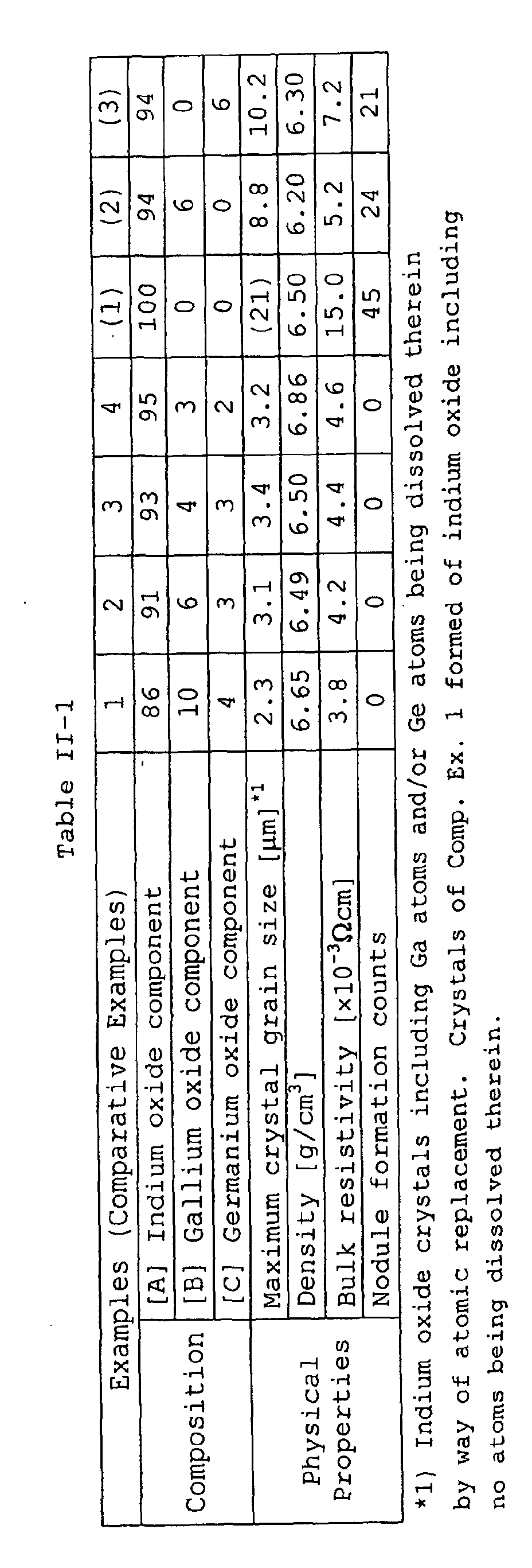
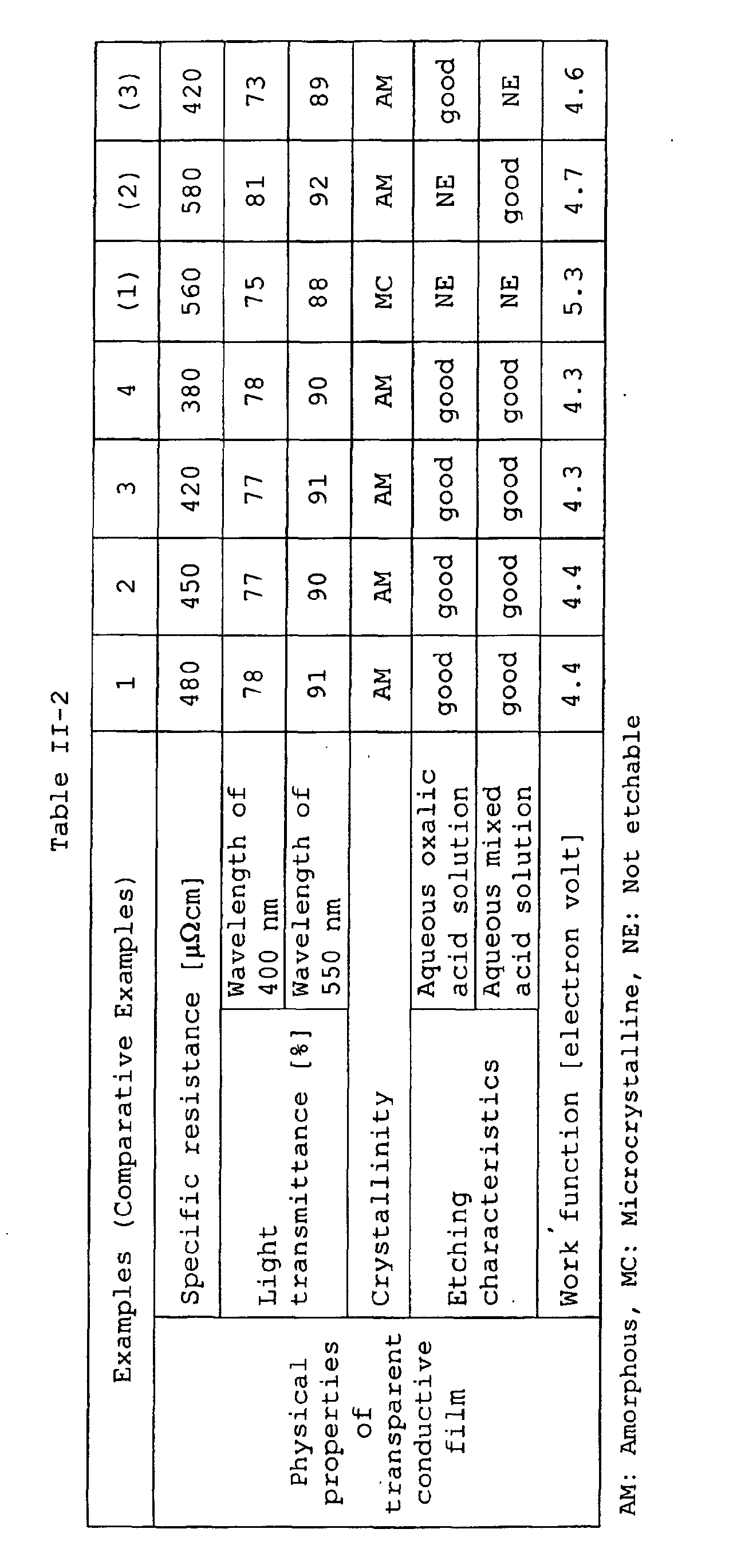
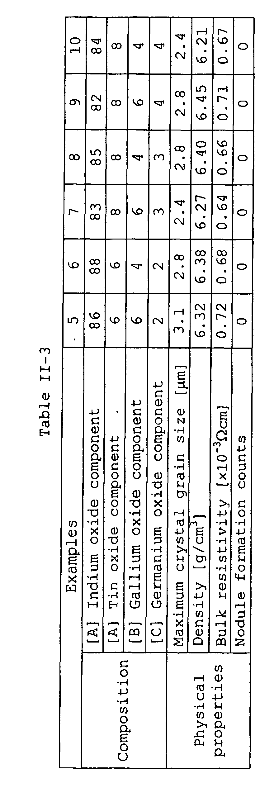
Technical Field
-
The present invention relates to a sputtering target
which inhibits formation of nodules during sputtering so as
to form a transparent conductive film, thereby reliably
forming the film, and to a transparent conductive film
exhibiting excellent etching processability.
Technical Field
-
By virtue of their excellent display performance and
small electric power consumption, liquid crystal display
devices and electroluminescence display devices are widely
employed as display units in cellular phones, personal
computers, word processors, television sets, etc. In any of
these apparatuses, such a display unit has a sandwich
structure in which a display element is sandwiched between
transparent conductive films. Among others, indium tin oxide
(hereinafter abbreviated as ITO) film is usually employed as
transparent conductive film used in these display units,
because ITO film exhibits excellent transparency and
conductivity, etching processability, and excellent adhesion
to a substrate. The ITO film is generally produced through
sputtering.
-
Although, as mentioned above, ITO film has excellent
performance as transparent conductive film, the film also has
a drawback. That is, when ITO film is formed through
sputtering of a sputtering target, black deposits
(protrusions) called nodules are formed on the surface of the
target, thereby reducing the film formation speed. Also,
discharge voltage is elevated, causing anomalous electric
discharge, and in this case, nodules scatter to deposit on a
substrate for film formation, thereby causing contamination
of the formed transparent conductive film. In the case in
which such nodules have been formed, film formation operation
must be stopped so as to remove nodules formed on the surface
of the target by polishing. Therefore, productivity of
transparent conductive film is detrimentally decreased.
-
In order to prevent contamination of transparent
conductive film caused by diffusion of nodules without
stopping operation of forming transparent conductive film,
there has been studied provision, in an electric power
circuit of a film formation apparatus, of means for
suppressing anomalous electric discharge. However, even when
the means is employed, formation of nodules has not been
prevented completely. For the purpose of prevention of
nodule formation, a target having a theoretical relative
density of about 99% has been produced through high-temperature
sintering so as to attain high density and reduce
pores. However, also in this case, nodule formation cannot
be prevented completely. Under such circumstances, it is
desired to develop a target for forming transparent
conductive film, which target can suppress formation of
nodules when the film is formed through sputtering and which
attains reliable formation of transparent conductive film.
-
From another aspect, the formed ITO film is etched by
use of a strong acid or aqua regia so as to form circuit
patterns. The etching raises a problem that aluminum serving
as a wiring material for fabricating a thin-film transistor
is generally corroded. Therefore, it is also desired to
develop a transparent conductive film which allows etching
without adversely affecting such a wiring material.
-
Thus, an object of the present invention is to provide
a sputtering target which suppresses formation of nodules
during sputtering so as to form a transparent conductive film,
thereby reliably forming the film. Another object of the
invention is to provide a transparent conductive film
exhibiting excellent etching processability.
Disclosure of the Invention
-
The present inventors have carried out extensive
studies in order to overcome the above drawbacks, and have
found that nodules formed on a target for forming ITO film
are basically attributed to unsputtered portions remaining on
the surface of the target, and that the ease of forming such
unsputtered portions depends on the crystal grain size of a
metal oxide constituting the target. Briefly, the inventors
have found that occurrence of nodule formation on the surface
of the target markedly increases when the crystal grain size
of indium oxide-a metal oxide constituting the
target-exceeds a specific grain size. The present
invention has been accomplished on the basis of these
findings. The present invention includes a first invention
and a second invention.
-
Accordingly, the gist of the first invention includes
the following:
- (1) a sputtering target formed of a sintered body of
metal oxide including indium oxide, gallium oxide, and zinc
oxide, wherein the metal oxide contains one or more hexagonal
layered compounds selected from the group consisting of
In2O3(ZnO)m (wherein m is an integer from 2 to 10), In2Ga2ZnO7,
InGaZnO4, InGaZn2O5, InGaZn3O6, InGaZn4O7, InGaZn5O8, InGaZn6O9,
and InGaZn7O10, and the sintered body is composed of indium
oxide in an amount of 90 to 99 mass% and a combination of
gallium oxide and zinc oxide in a total amount of 1 to 10
mass%;
- (2) a sputtering target as described in (1) above,
wherein the sintered body of metal oxide is composed of
indium oxide in an amount of 90 to 98 mass% and a combination
of gallium oxide and zinc oxide in a total amount of 2 to 10
mass%;
- (3) a sputtering target as described in (1) above,
wherein the sintered body of metal oxide is composed of
indium oxide in an amount of 92 to 97 mass% and a combination
of gallium oxide and zinc oxide in a total amount of 3 to 8
mass%;
- (4) a sputtering target as described in any of (1) to
(3) above, wherein the hexagonal layered compounds have a
maximum crystal grain size of 5 µm or less;
- (5) a sputtering target as described in (4) above,
wherein the maximum crystal grain size is 3 µm or less;
- (6) a sputtering target formed of a sintered body of
metal oxide including indium oxide, tin oxide, gallium oxide,
and zinc oxide, wherein the metal oxide contains one or more
hexagonal layered compounds selected from the group
consisting of In2O3(ZnO)m (wherein m is an integer from 2 to
10), In2Ga2ZnO7, InGaZnO4, InGaZn2O5, InGaZn3O6, InGaZn4O7,
InGaZn5O8, InGaZn6O9, and InGaZn7O10, and the sintered body is
composed of indium oxide in an amount of 70 to 94 mass%, tin
oxide in an amount of 5 to 20 mass%, and a combination of
gallium oxide and zinc oxide in a total amount of 1 to 10
mass%;
- (7) a sputtering target as described in (6) above,
wherein the sintered body of metal oxide is composed of
indium oxide in an amount of 75 to 93 mass%, tin oxide in an
amount of 5 to 15 mass%, and a combination of gallium oxide
and zinc oxide in a total amount of 2 to 10 mass%;
- (8) a sputtering target as described in (6) above,
wherein the sintered body of metal oxide is composed of
indium oxide in an amount of 80 to 90 mass%, tin oxide in an
amount of 7 to 12 mass%, and a combination of gallium oxide
and zinc oxide in a total amount of 3 to 8 mass%;
- (9) a sputtering target as described in any of (6) to
(8) above, wherein the hexagonal layered compounds have a
maximum crystal grain size of 5 µm or less;
- (10) a sputtering target as described in (9) above,
wherein the maximum crystal grain size is 3 µm or less;
- (11) a transparent conductive film formed of a metal
oxide including indium oxide, gallium oxide, and zinc oxide,
wherein the metal oxide is composed of indium oxide in an
amount of 90 to 99 mass% and a combination of gallium oxide
and zinc oxide in a total amount of 1 to 10 mass%;
- (12) a transparent conductive film as described in (11)
above, wherein the metal oxide is composed of indium oxide in
an amount of 90 to 98 mass% and a combination of gallium
oxide and zinc oxide in a total amount of 2 to 10 mass%;
- (13) a transparent conductive film as described in (11)
above, wherein the metal oxide is composed of indium oxide in
an amount of 92 to 97 mass% and a combination of gallium
oxide and zinc oxide in a total amount of 3 to 8 mass%;
- (14) a transparent conductive film formed of a metal
oxide including indium oxide, tin oxide, gallium oxide, and
zinc oxide, wherein the metal oxide is composed of indium
oxide in an amount of 70 to 94 mass%, tin oxide in an amount
of 5 to 20 mass%, and a combination of gallium oxide and zinc
oxide in a total amount of 1 to 10 mass%;
- (15) a transparent conductive film as described in (14)
above, wherein the metal oxide is composed of indium oxide in
an amount of 75 to 93 mass%, tin oxide in an amount of 5 to
15 mass%, and a combination of gallium oxide and zinc oxide
in a total amount of 2 to 10 mass%;
- (16) a transparent conductive film as described in (14)
above, wherein the metal oxide is composed of indium oxide in
an amount of 80 to 90 mass%, tin oxide in an amount of 7 to
12 mass%, and a combination of gallium oxide and zinc oxide
in a total amount of 3 to 8 mass%;
- (17) a transparent conductive film which is produced by
subjecting a transparent conductive film as recited in any of
(14) to (16) above to heat treatment at 230°C or higher;
- (18) a transparent conductive film which is produced by
subjecting a transparent conductive film as recited in any of
(14) to (16) above to patterning and subsequent heat
treatment at 230°C or higher; and
- (19) a method for producing a transparent conductive
film characterized in that the method comprises sputtering a
sputtering target as recited in any of (1) to (10) above for
forming film.
-
-
The gist of the second invention includes the
following:
- (1) a sputtering target formed of a sintered body of
metal oxide comprising indium oxide (a1) [A1] in an amount of
85 to 99 mass% and a combination of gallium oxide [B] and
germanium oxide [C] in a total amount of 1 to 15 mass%,
wherein at least the indium oxide present in the sintered
body includes gallium atoms and germanium atoms, the two
atomic species being dissolved therein by way of atomic
replacement;
- (2) a sputtering target as described in (1) above,
wherein the sputtering target is formed of the sintered body
of metal oxide composed of the component [A1] in an amount of
90 to 97 mass% and a combination of the component [B] and the
component [C] in a total amount of 3 to 10 mass%;
- (3) a sputtering target as described in (1) or (2)
above, wherein indium oxide crystals including the gallium
atoms or indium oxide crystals including the germanium atoms,
the two atomic species being dissolved therein by way of
atomic replacement, have a maximum grain size of 5 µm or
less;
- (4) a sputtering target as described in (3) above,
wherein the maximum grain size is 3 µm or less;
- (5) a sputtering target formed of a sintered body of
metal oxide comprising a combination of indium oxide (a2) and
tin oxide (a3) [A2] in a total amount of 90 to 99 mass% and a
combination of gallium oxide [B] and germanium oxide [C] in a
total amount of 1 to 10 mass%, wherein at least the indium
oxide present in the sintered body includes tin atoms,
gallium atoms, and germanium atoms, the three atomic species
being dissolved therein by way of atomic replacement;
- (6) a sputtering target as described in (5) above,
wherein the sputtering target is formed of the sintered body
of metal oxide composed of the component [A2] in an amount of
90 to 98 mass% and a combination of the component [B] and the
component [C] in a total amount of 2 to 10 mass%;
- (7) a sputtering target as described in (5) above,
wherein the sputtering target is formed of the sintered body
of metal oxide composed of the component [A2] in an amount of
92 to 97 mass% and a combination of the component [B] and the
component [C] in a total amount of 3 to 8 mass%;
- (8) a sputtering target as described in any of (5) to
(7) above, wherein indium oxide crystals including tin atoms,
indium oxide crystals including gallium atoms, or indium
oxide crystals including germanium atoms, the three atomic
species being dissolved therein by way of atomic replacement,
have a maximum grain size of 5 µm or less;
- (9) a sputtering target as described in (8) above,
wherein the maximum grain size is 3 µm or less;
- (10) a transparent conductive film formed of a metal
oxide comprising indium oxide (a1) [A1] in an amount of 85 to
99 mass% and a combination of gallium oxide [B] and germanium
oxide [C] in a total amount of 1 to 10 mass%, wherein at
least the indium oxide present in a sintered body serving as
the source of the film includes gallium atoms and germanium
atoms, the two atomic species being dissolved therein by way
of atomic replacement;
- (11) a transparent conductive film as described in (10)
above, wherein the film is formed of a metal oxide composed
of the component [A1] in an amount of 90 to 97 mass% and a
combination of the component [B] and the component [C] in a
total amount of 3 to 10 mass%;
- (12) a transparent conductive film formed of a metal
oxide comprising a combination of indium oxide (a2) and tin
oxide (a3) [A2] in a total amount of 90 to 99 mass% and a
combination of gallium oxide [B] and germanium oxide [C] in a
total amount of 1 to 10 mass%, wherein at least the indium
oxide present in a sintered body serving as the source of the
film includes tin atoms, gallium atoms, and germanium atoms,
the three atomic species being dissolved therein by way of
atomic replacement;
- (13) a transparent conductive film as described in (12)
above, wherein the film is formed of a metal oxide composed
of the component [A2] in an amount of 90 to 98 mass% and a
combination of the component [B] and the component [C] in a
total amount of 2 to 10 mass%;
- (14) a transparent conductive film as described in (12)
above, wherein the film is formed of a metal oxide composed
of the component [A2] in an amount of 92 to 97 mass% and a
combination of the component [B] and the component [C] in a
total amount of 3 to 8 mass%;
- (15) a transparent conductive film which is produced by
subjecting a transparent conductive film as recited in any of
(12) to (14) above to heat treatment at 230°C or higher; and
- (16) a method for producing a transparent conductive
film characterized in that the method comprises sputtering a
sputtering target as recited in any of (1) to (9) above for
forming film.
-
Best Modes for Carrying Out the Invention
-
Embodiments of the present invention will next be
described.
[I] First invention
-
The sputtering target according to the first invention
(in this section, hereinafter "the first invention" may be
referred to simply as "the present invention") is formed of a
sintered body of metal oxide including indium oxide, gallium
oxide, and zinc oxide, wherein the metal oxide contains one
or more hexagonal layered compounds selected from the group
consisting of In2O3(ZnO)m (wherein m is an integer from 2 to
10), In2Ga2ZnO7, InGaZnO4, InGaZn2O5, InGaZn3O6, InGaZn4O7,
InGaZn5O8, InGaZn6O9, and InGaZn7O10, and the sintered body is
composed of indium oxide in an amount of 90 to 99 mass% and a
combination of gallium oxide and zinc oxide in a total amount
of 1 to 10 mass%.
-
Among hexagonal layered compounds which are contained
in the metal oxide formed of indium oxide, gallium oxide, and
zinc oxide, the metal oxide represented by formula In2O3(ZnO)m
may be any of compounds in which m is any integer from 2 to
10. However, among them, those having an m value of 2 to 7
are more preferred, from the viewpoint of low volume
resistivity.
-
The metal oxide formed of indium oxide, gallium oxide,
and zinc oxide is composed of indium oxide in an amount of 90
to 99 mass% and a combination of gallium oxide and zinc oxide
in a total amount of 1 to 10 mass%. The reasons why the
metal oxide has the foregoing composition are as follows.
When the total amount of gallium oxide and zinc oxide is less
than 1 mass%, etching processability of the transparent
conductive film obtained by sputtering the sputtering target
is reduced, whereas when the total amount of gallium oxide
and zinc oxide is in excess of 10 mass%, conductivity of the
obtained transparent conductive film decreases. Regarding
the composition of the metal oxide, the amount of indium
oxide and the total amount of gallium oxide and zinc oxide
are preferably 90 to 98 mass% and 2 to 10 mass%, respectively,
more preferably 92 to 97 mass% and 3 to 8 mass%, respectively.
-
Preferably, the amount of gallium oxide contained in
the metal oxide is equal to or greater than that of zinc
oxide contained in the metal oxide, since the transparent
conductive film obtained by sputtering the sputtering target
has excellent transparency. The gallium oxide content is
more preferably at least 1.5 times the zinc oxide content,
further more preferably at least twice the zinc oxide content.
-
The hexagonal layered compounds contained in the metal
oxide preferably have a maximum crystal grain size of 5 µm or
less. This is because, in the sintered body of the metal
oxide, when the maximum crystal grain size of the hexagonal
layered compounds present in the grain boundary of indium
oxide crystals is controlled to 5 µm or less, growth of
indium oxide crystals in contact with the hexagonal layered
compounds can be suppressed, and the maximum grain size of
indium oxide crystals can be controlled to 10 µm or less.
Thus, more preferably, the maximum crystal grain size of the
hexagonal layered compounds is controlled to 3 µm or less,
whereby the maximum grain size of indium oxide crystals
present in the sintered body can be controlled to 7 µm or
less. Thus, when the grain size of the crystals present in
the sintered body of metal oxide is reduced, nodule formation
can be prevented during film formation by sputtering the
sputtering target formed of the sintered body. From another
aspect, the effect of reducing the grain size of indium oxide
crystals can be enhanced as the hexagonal layered compound
content is elevated. However, since conductivity of the
transparent conductive film obtained by sputtering the
sputtering target decreases in this case, the hexagonal
layered compounds are formed in amounts corresponding to a
total amount of gallium oxide and zinc oxide of 10 mass% or
less.
-
Meanwhile, hexagonal layered compounds present in the
metal oxide can be identified through analysis; for example,
X-ray diffraction analysis or EPMA (Electron Probe Micro-Analysis).
The maximum grain size of hexagonal layered
compound crystals is determined through the following
procedure. After the surface of the sputtering target has
been polished, the surface is observed at five points under a
scanning electron microscope at a magnification of ×2,500.
In the case where the sputtering target has a circular cross-section,
the five points include the center of the circle
(one point) and midpoints (four points) between the periphery
and the center, the midpoints located on two lines which
intersect each other at right angle at the center. In the
case where the sputtering target has a square cross-section,
the five points include the center of the square (one point)
and respective midpoints (four points) between the vertices
and the center, the midpoints located on the two diagonals
which intersect each other at the center. The longest
diameter of the largest grain observed at each point (frame
of 50 µm × 50 µm) is measured, and the longest diameter
values measured in the five frames are averaged.
-
Alternatively, the sputtering target according to the
present invention may be formed of a sintered body of 4-component
metal oxide including indium oxide, tin oxide,
gallium oxide, and zinc oxide, wherein the metal oxide
contains one or more hexagonal layered compounds selected
from the group consisting of In2O3(ZnO)m (wherein m is an
integer from 2 to 10), In2Ga2ZnO7, InGaZnO4, InGaZn2O5,
InGaZn3O6, InGaZn4O7, InGaZn5O8, InGaZn6O9, and InGaZn7O10, and
the sintered body is composed of indium oxide in an amount of
70 to 94 mass%, tin oxide in an amount of 5 to 20 mass%, and
a combination of gallium oxide and zinc oxide in a total
amount of 1 to 10 mass%.
-
The amount of the tin oxide component present in the
sputtering target formed of a sintered body of a 4-component
metal oxide is controlled to 5 to 20 mass%. The reasons why
the target has the foregoing composition are as follows.
When the tin oxide content is less than 5 mass%, electric
resistance of the sputtering target may fail to sufficiently
decrease, whereas when the tin oxide content is in excess of
20 mass%, the electric resistance may excessively increase.
Thus, the tin oxide content of the sintered body is more
preferably 5 to 15 mass%, further more preferably 7 to 12
mass%. Furthermore, the total amount of the gallium oxide
component and the zinc oxide component contained in the
sputtering target is controlled to 1 to 10 mass%. The
criteria of the amount are as follows. When the total amount
of gallium oxide and zinc oxide is less than 1 mass%, the
produced transparent conductive film has a crystalline nature,
thereby reducing etching processability, whereas when the
total amount of gallium oxide and zinc oxide is in excess of
10 mass%, conductivity of the obtained transparent conductive
film decreases.
-
The metal oxide constituting the sputtering target
formed of the sintered body of a 4-component metal oxide is
preferably composed of indium oxide in an amount of 75 to 93
mass%, tin oxide in an amount of 5 to 15 mass%, and a
combination of gallium oxide and zinc oxide in a total amount
of 2 to 10 mass%. More preferably, the metal oxide is
composed of indium oxide in an amount of 80 to 90 mass%, tin
oxide in an amount of 7 to 12 mass%, and a combination of
gallium oxide and zinc oxide in a total amount of 3 to 8
mass%.
-
Preferably, the amount of tin oxide contained in the
sputtering target is greater than that of zinc oxide
contained in the sputtering target, since conductivity of the
transparent conductive film obtained by sputtering the
sputtering target can be enhanced. The tin oxide content is
preferably at least 1.5 times the zinc oxide content, more
preferably at least twice the zinc oxide content.
-
The hexagonal layered compounds contained in the
sputtering target preferably have a maximum crystal grain
size of 5 µm or less. This is because, in the sintered body
of the metal oxide, by controlling the maximum crystal grain
size of the hexagonal layered compounds present in the grain
boundary of indium oxide crystals to 5 µm or less, growth of
indium oxide crystals in contact with the hexagonal layered
compounds can be suppressed, and the maximum grain size of
indium oxide crystals can be suppressed to 10 µm or less.
More preferably, the maximum crystal grain size of the
hexagonal layered compounds is controlled to 3 µm or less,
whereby the maximum grain size of indium oxide crystals
present in the sintered body can be suppressed to 7 µm or
less. Thus, when the grain size of indium oxide crystals
present in the sintered body constituting the sputtering
target is reduced, nodule formation can be prevented during
film formation.
-
Next, the sputtering target can be produced through,
for example, the following procedure. Powders of indium
oxide, gallium oxide, zinc oxide, and optional tin oxide are
mixed and pulverized, to thereby produce fine powder. The
fine powder is granulated through casting or spray drying,
and the formed granules are press-molded and sintered. The
sintered body is cut, to thereby produce the sputtering
target. Mixing and pulverization of metal oxides serving as
raw materials can be performed by means of a wet-type mixing-pulverizer;
e.g., a wet ball mill or a beads mill, or through
ultrasonication. Raw material powders are preferably
pulverized so that the pulverized product has a mean particle
size of 1 µm or less.
-
The above metal oxide is fired in air or an oxygen-containing
atmosphere at 1,300 to 1,700°C, preferably 1,450
to 1,600°C for 2 to 36 hours, preferably 4 to 24 hours. The
temperature elevation rate during firing preferably falls
within a range of 2 to 10 °C/min. The thus-obtained sintered
body is cut, to thereby form sputtering target having a
suitable shape adaptable to a sputtering apparatus. The
target is attached to a jig for placing the target in the
sputtering apparatus.
-
The transparent conductive film according to the
present invention is formed on a substrate by sputtering the
aforementioned sputtering target. A substrate of high
transparency is preferably employed as the substrate, and
conventionally used glass substrates and transparent
synthetic resin film and sheets can be employed. Examples of
the synthetic resin to be employed include polycarbonate
resin, poly(methyl methacrylate) resin, polyester resin,
polyether sulfone resin, and polyarylate resins.
-
A variety of sputtering apparatuses can be employed for
forming the transparent conductive film through sputtering.
Particularly, a magnetron sputtering apparatus is preferably
used. When such a magnetron sputtering apparatus is used,
plasma power-one of the sputtering conditions for forming
a film-varies depending on the surface area of the target
employed and the thickness of the transparent conductive film
to be produced. However, a transparent conductive film
having a desired film thickness can be produced generally
under the following sputtering conditions: plasma power; 0.3
to 4 W/cm2 (i.e., 1 cm2 of the surface area of the target),
and film formation time; 5 to 120 minutes. The thickness of
the transparent conductive film, which varies depending on
the display apparatus to which the film is applied, is
generally 200 to 6,000 Å, preferably 300 to 2,000 Å.
-
The thus-produced transparent conductive film of the
present invention is formed of a metal oxide including indium
oxide, gallium oxide, and zinc oxide, wherein the metal oxide
is composed of indium oxide in an amount of 90 to 99 mass%
and a combination of gallium oxide and zinc oxide in a total
amount of 1 to 10 mass%.
-
Since the transparent conductive film is formed of a
metal oxide composed of indium oxide in an amount of 90 to 99
mass% and a combination of gallium oxide and zinc oxide in a
total amount of 1 to 10 mass%, the film exhibits excellent
transparency and conductivity and has excellent etching
characteristics by virtue of its amorphous nature. When the
total amount of gallium oxide and zinc oxide is less than 1
mass%, the transparent conductive film has a crystalline
nature, thereby reducing etching processability, whereas when
the total amount of gallium oxide and zinc oxide is in excess
of 10 mass%, conductivity of the transparent conductive film
decreases. In addition, the transparent conductive film
preferably has a composition in which the amount of indium
oxide and the total amount of gallium oxide and zinc oxide
are 90 to 98 mass% and 2 to 10 mass%, respectively, from the
viewpoint of more excellent conductivity and etching
characteristics. More preferably, the film has a composition
in which the amount of indium oxide and the total amount of
gallium oxide and zinc oxide are 92 to 97 mass% and 3 to 8
mass%, respectively.
-
The transparent conductive film of the present
invention is formed of a 4-component metal oxide including
indium oxide, tin oxide, gallium oxide, and zinc oxide,
wherein the metal oxide is composed of indium oxide in an
amount of 70 to 94 mass%, tin oxide in an amount of 5 to 20
mass%, and a combination of gallium oxide and zinc oxide in a
total amount of 1 to 10 mass%.
-
Since the transparent conductive film is formed of the
4-component metal oxide including indium oxide, tin oxide,
gallium oxide, and zinc oxide, wherein the metal oxide is
composed of indium oxide in an amount of 70 to 94 mass%, tin
oxide in an amount of 5 to 20 mass%, and a combination of
gallium oxide and zinc oxide in a total amount of 1 to 10
mass%, the film exhibits excellent transparency and
conductivity and has excellent etching characteristics by
virtue of its amorphous nature. Herein, the amount of the
tin oxide component present in the transparent conductive
film is controlled to 5 to 20 mass%. This is because, when
the tin oxide content is less than 5 mass%, electric
resistance of the film may fail to decrease, whereas when the
tin oxide content is in excess of 20 mass%, the electric
resistance of the transparent conductive film may increase.
Thus, the tin oxide content of the sintered body is more
preferably 5 to 15 mass%, further more preferably 7 to 12
mass%.
-
Preferably, the amount of tin oxide contained in the
transparent conductive film formed of a 4-component metal
oxide is greater than that of zinc oxide from the viewpoint
of excellent conductivity. The tin oxide content of the
transparent conductive film is more preferably at least 1.5
times the zinc oxide content, further more preferably at
least twice the zinc oxide content.
-
The total amount of gallium oxide and zinc oxide
contained in the transparent conductive film formed of the
metal oxide is controlled to 1 to 10 mass%. The criteria of
the amount are as follows. When the total amount of gallium
oxide and zinc oxide is less than 1 mass%, the transparent
conductive film has a crystalline nature, thereby reducing
etching processability, whereas when the total amount is in
excess of 10 mass%, conductivity of the transparent
conductive film decreases. The total amount of gallium oxide
and zinc oxide contained in the transparent conductive film
is preferably 2 to 10 mass%, more preferably 3 to 8 mass%.
-
When the amorphous transparent conductive film formed
of the 4-component metal oxide is subjected to heat treatment
at 230°C or higher after film formation, the transparent
conductive film becomes crystalline, thereby producing a
transparent conductive film having higher conductivity. The
heat treatment is preferably performed at 250°C or higher,
more preferably 260°C or higher. In this case, the heat
treatment is performed for 0.1 to five hours. The heat
treatment is performed preferably after completion of
patterning of the amorphous transparent conductive film
obtained by sputtering the sputtering target. The patterning
can be performed through a conventional method such as
photolithography.
-
The thus-produced transparent conductive film is
endowed with excellent light transmittance; i.e., about 75%
for a beam of 400 nm and about 90% for a beam of 550 nm; high
conductivity; and a work function of 4.6 eV or lower. Thus,
when the film is used in an organic electroluminescence
element, contact resistance with an electron injection layer
can be lowered. Accordingly, the transparent conductive film
of the present invention is suitably employed as a
transparent electrode used in a variety of display devices
such as liquid crystal display devices and organic
electroluminescence display elements, which are required to
have high transparency and conductivity.
-
The present invention will next be described in more
detail by way of Examples and Comparative Examples.
[Example I-1]
(1) Production of sputtering target
-
Indium oxide powder, gallium oxide powder, and zinc
oxide powder, serving as raw materials, were mixed such that
the compositional proportions of the components were adjusted
to 93 mass%, 4 mass%, and 3 mass%, respectively. The thus-prepared
metal oxide powder mixture was fed to a wet ball
mill and pulverized through mixing for 10 hours, to thereby
form a raw material powder having a mean particle size of 1.8
to 2 µm. The thus-formed raw material powder was dried and
granulated by means of a spray drier. The resultant granules
were charged into a metal mold and press-molded by means of a
presser, to thereby obtain a molded disk (diameter: 10 cm,
thickness: 5 mm).
-
The obtained molded disk was placed in a sintering
furnace and sintered in a pressurized oxygen gas atmosphere
for six hours, while the sintering temperature was maintained
within a range of 1,420 to 1,480°C.
-
Analysis X-ray diffractometry and EPMA of the above
sintered body revealed that hexagonal layered compounds
represented by In2O3(ZnO)4 or InGaZnO4 had been formed in the
sintered body. The maximum crystal grain size of the
sintered body was determined to be 2.8 µm through the
following procedure. Briefly, the sintered disk product was
photographed at five points under a scanning electron
microscope at a magnification of ×2,500, wherein the five
points included the center of the circle (one point) and
midpoints (four points) between the periphery and the center,
the midpoints located on two lines which intersect each other
at right angle at the center. The longest diameter of the
largest grain observed at each point (frame of 50 µm × 50 µm)
was measured, and the longest diameter values measured in the
five frames were averaged. The sintered body was found to
have a density of 6.6 g/cm3, which is 94% the corresponding
theoretical density. The bulk resistivity of the sintered
body, as determined through the four-probe method, was found
to be 2.4 × 10⁻³ Ω·cm.
-
The thus-produced sintered body was cut, to thereby
produce a sputtering target having a diameter of about 10 cm
and a thickness of about 5 mm.
(2) Observation of nodule formation
-
The sputtering target which had been produced in (1)
above was bonded to a copper plate and set in a DC magnetron
sputtering apparatus. Sputtering was performed continuously
for 30 hours in an atmosphere of a mixture gas of argon
containing 3% hydrogen. Other sputtering conditions employed
were as follows: pressure; 3 × 10⁻¹ Pa, base pressure; 5 × 10
4 Pa, substrate temperature; 25°C, and input power; 100 W.
Notably, the hydrogen was added to the atmosphere so as to
promote formation of nodules.
-
The surface conditions of the target after sputtering
were observed under a stereoscopic microscope at a
magnification of ×50, and the following procedure was
employed: counting the number of nodules having a size of 20
µm or greater formed in each field of vision (3 mm2) and
averaging the values. Through this procedure, no nodule was
identified on the surface of the sputtering target used
herein.
-
The composition, physical properties, and observation
regarding nodule formation of the sputtering target produced
in Example I-1 are shown in Table I-1.
-
In the Table, "Example I-1" is abbreviated as "Example
1" for the sake of convenience. The same convention is
applied to other Examples and Comparative Examples and to
Tables I-1 to I-6.
(3) Production of transparent conductive film
-
The sputtering target which had been produced in (1)
above was set in a DC magnetron sputtering apparatus.
Transparent conductive film was formed on a glass substrate
by sputtering the target at room temperature. The sputtering
conditions employed were as follows: atmosphere; mixture gas
of argon containing a small amount of oxygen, sputtering
pressure; 3 × 10⁻¹ Pa, base pressure; 5 × 10⁻⁴ Pa, substrate
temperature; 25°C, input power; 100 W, and sputtering time;
20 minutes.
-
As a result, a transparent conductive film having a
thickness of about 2,000 Å was formed on the glass substrate,
whereby a transparent glass plate was produced.
(4) Evaluation of transparent conductive film
-
The transparent conductive film serving as a surface
layer of the transparent conductive glass plate obtained in
(3) above was evaluated in terms of the following properties.
The results are shown in Table I-2.
(1) Conductivity
-
As an index for conductivity, specific resistance of
the transparent conductive film was measured through the
four-probe method and found to be 290 × 10-6 Ω·cm.
(2) Transparency
-
As an index for transparency, light transmittance of
the film was measured by means of a spectrophotometer and
found to be 75% for a beam of 400 nm and 91% for a beam of
550 nm.
(3) Crystallinity
-
Crystallinity of the film was determined through X-ray
diffractometry, revealing that the transparent conductive
film was amorphous.
(4) Etching characteristics
-
In order to investigate etching characteristics of the
film, etching was performed at 30°C by use of a 3.5 mass%
aqueous oxalic acid solution as an etchant. The etched
surface conditions of the transparent conductive film after
etching were observed under a spectroscopic microscope. No
etching residue was observed on the etched surface of the
transparent conductive film.
-
The above procedure was repeated, except that a mixed
acid (nitric acid : phosphoric acid : acetic acid : water =
2 : 17 : 1,800 : 1,000) was employed as an etchant, to
thereby evaluate etching characteristics. No etching residue
was observed on the etched surface of the transparent
conductive film.
(5) Work function
-
Work function of the transparent conductive film was
measured through atmospheric ultraviolet photoelectron
spectroscopy and was found to be 4.38 eV.
[Example I-2]
(1) Production of sputtering target and observation of nodule
formation
-
The procedure of Example I-1 (1) was repeated, except
that indium oxide, gallium oxide, and zinc oxide were used as
raw materials in amounts of 91 parts by mass, 6 parts by mass,
and 3 parts by mass, respectively, to thereby produce a
sputtering target. In the produced sputtering target,
formation of a hexagonal layered compound represented by
In2Ga2ZnO7 was confirmed.
-
In a manner similar to that employed in Example I-1 (2),
the sputtering target was observed so as to identify nodule
formation during sputtering.
-
The composition, physical properties, and observation
regarding nodule formation of the sputtering target are shown
in Table I-1.
(2) Production and evaluation of transparent conductive film
-
The procedure of Example I-1 (3) was repeated, except
that the sputtering target which had been produced in (1)
above was sputtered, to thereby produce a transparent
conductive film.
-
In a manner similar to that employed in Example I-1 (4),
the transparent conductive film was evaluated. The results
are shown in Table I-2.
[Example I-3]
(1) Production of sputtering target and observation of nodule
formation
-
The procedure of Example I-1 (1) was repeated, except
that indium oxide, gallium oxide, and zinc oxide were used as
raw materials in amounts of 94 parts by mass, 4 parts by mass,
and 2 parts by mass, respectively, to thereby produce a
sputtering target. In the produced sputtering target,
formation of a hexagonal layered compound represented by
InGaZnO4 was confirmed.
-
In a manner similar to that employed in Example I-1 (2),
the sputtering target was observed so as to identify nodule
formation during sputtering.
-
The composition, physical properties, and observation
regarding nodule formation of the sputtering target are shown
in Table I-1.
(2) Production and evaluation of transparent conductive film
-
The procedure of Example I-1 (3) was repeated, except
that the sputtering target which had been produced in (1)
above was sputtered, to thereby produce a transparent
conductive film.
-
In a manner similar to that employed in Example I-1 (4),
the transparent conductive film was evaluated. The results
are shown in Table I-2.
[Example I-4]
(1) Production of sputtering target and observation of nodule
formation
-
The procedure of Example I-1 (1) was repeated, except
that indium oxide, gallium oxide, and zinc oxide were used as
raw materials in amounts of 92 parts by mass, 6 parts by mass,
and 2 parts by mass, respectively, to thereby produce a
sputtering target. In the produced sputtering target,
formation of a hexagonal layered compound represented by
In2Ga2ZnO7 was confirmed.
-
In a manner similar to that employed in Example I-1 (2),
the sputtering target was observed so as to identify nodule
formation during sputtering.
-
The composition, physical properties, and observation
regarding nodule formation of the sputtering target are shown
in Table I-1.
(2) Production and evaluation of transparent conductive film
-
The procedure of Example I-1 (3) was repeated, except
that the sputtering target which had been produced in (1)
above was sputtered, to thereby produce a transparent
conductive film.
-
In a manner similar to that employed in Example I-1 (4),
the transparent conductive film was evaluated. The results
are shown in Table I-2.
[Comparative Example I-1]
(1) Production of sputtering target and observation of nodule
formation
-
The procedure of Example I-1 (1) was repeated, except
that indium oxide (90 parts by mass) and gallium oxide (10
parts by mass) were used as raw materials, to thereby produce
a sputtering target. In the produced sputtering target,
formation of a hexagonal layered compound was not confirmed.
-
In a manner similar to that employed in Example I-1 (2),
the sputtering target was observed so as to identify nodule
formation during sputtering. Through observation at a
magnification of ×50, 21 nodules were identified in a field
of vision (3 mm2) on the surface of the sputtering target
after completion of sputtering for continuous 30 hours.
-
The composition, physical properties, and observation
regarding nodule formation of the sputtering target are shown
in Table I-1.
(2) Production and evaluation of transparent conductive film
-
The procedure of Example I-1 (3) was repeated, except
that the sputtering target which had been produced in (1)
above was sputtered, to thereby produce a transparent
conductive film.
-
In a manner similar to that employed in Example I-1 (4),
the transparent conductive film was evaluated. The results
are shown in Table I-2.
[Comparative Example I-2]
(1) Production of sputtering target and observation of nodule
formation
-
The procedure of Example I-1 (1) was repeated, except
that indium oxide and zinc oxide were used as raw materials
in amounts of 90 parts by mass and 10 parts by mass,
respectively, to thereby produce a sputtering target. In the
produced sputtering target, formation of a hexagonal layered
compound represented by In2O3(ZnO)7 was confirmed.
-
In a manner similar to that employed in Example I-1 (2),
the sputtering target was observed so as to identify nodule
formation during sputtering. Through observation at a
magnification of ×50, no nodule was identified in a field of
vision (3 mm2) on the surface of the sputtering target after
completion of sputtering for continuous 30 hours.
-
The composition, physical properties, and observation
regarding nodule formation of the sputtering target are shown
in Table I-1.
(2) Production and evaluation of transparent conductive film
-
The procedure of Example I-1 (3) was repeated, except
that the sputtering target which had been produced in (1)
above was sputtered, to thereby produce a transparent
conductive film.
-
In a manner similar to that employed in Example I-1 (4),
the transparent conductive film was evaluated. The results
are shown in Table I-2.
[Comparative Example I-3]
(1) Production of sputtering target and observation of nodule
formation
-
The procedure of Example I-1 (1) was repeated, except
that indium oxide and gallium oxide were used as raw
materials in amounts of 95 parts by mass and 5 parts by mass,
respectively, to thereby produce a sputtering target. In the
produced sputtering target, formation of a hexagonal layered
compound was not confirmed.
-
In a manner similar to that employed in Example I-1 (2),
the sputtering target was observed so as to identify nodule
formation during sputtering. Through observation at a
magnification of ×50, 32 nodules were identified in a field
of vision (3 mm2) on the surface of the sputtering target
after completion of sputtering for continuous 30 hours.
-
The composition, physical properties, and observation
regarding nodule formation of the sputtering target are shown
in Table I-1.
(2) Production and evaluation of transparent conductive film
-
The procedure of Example I-1 (3) was repeated, except
that the sputtering target which had been produced in (1)
above was sputtered, to thereby produce a transparent
conductive film.
-
In a manner similar to that employed in Example I-1 (4),
the transparent conductive film was evaluated. The results
are shown in Table I-2.
[Comparative Example I-4]
(1) Production of sputtering target and observation of nodule
formation
-
The procedure of Example I-1 (1) was repeated, except
that indium oxide and zinc oxide were used as raw materials
in amounts of 97 parts by mass and 3 parts by mass,
respectively, to thereby produce a sputtering target. In the
produced sputtering target, formation of a hexagonal layered
compound represented by In2O3(ZnO)4 was confirmed.
-
In a manner similar to that employed in Example I-1 (2),
the sputtering target was observed so as to identify nodule
formation during sputtering. Through observation at a
magnification of ×50, 12 nodules were identified in a field
of vision (3 mm2) on the surface of the sputtering target
after completion of sputtering for continuous 30 hours.
-
The composition, physical properties, and observation
regarding nodule formation of the sputtering target are shown
in Table I-1.
(2) Production and evaluation of transparent conductive film
-
The procedure of Example I-1 (3) was repeated, except
that the sputtering target which had been produced in (1)
above was sputtered, to thereby produce a transparent
conductive film.
-
In a manner similar to that employed in Example I-1 (4),
the transparent conductive film was evaluated. The results
are shown in Table I-2.
[Example I-5]
(1) Production of sputtering target and observation of nodule
formation
-
The procedure of Example I-1 (1) was repeated, except
that indium oxide, tin oxide, gallium oxide, and zinc oxide
were used as raw materials in amounts of 86 parts by mass, 6
parts by mass, 6 parts by mass, and 2 parts by mass,
respectively, to thereby produce a sputtering target. In the
produced sputtering target, formation of a hexagonal layered
compound represented by In2Ga2ZnO7 was confirmed.
-
In a manner similar to that employed in Example I-1 (2),
the sputtering target was observed so as to identify nodule
formation during sputtering.
-
The composition, physical properties, and observation
regarding nodule formation of the sputtering target are shown
in Table I-3.
(2) Production and evaluation of transparent conductive film
-
The procedure of Example I-1 (3) was repeated, except
that the sputtering target which had been produced in (1)
above was sputtered, to thereby produce a transparent
conductive film.
-
In a manner similar to that employed in Example I-1 (4),
the transparent conductive film was evaluated. The results
are shown in Table I-4.
[Example I-6]
(1) Production of sputtering target and observation of nodule
formation
-
The procedure of Example I-1 (1) was repeated, except
that indium oxide, tin oxide, gallium oxide, and zinc oxide
were used as raw materials in amounts of 86 parts by mass, 6
parts by mass, 4 parts by mass, and 2 parts by mass,
respectively, to thereby produce a sputtering target. In the
produced sputtering target, formation of a hexagonal layered
compound represented by In2Ga2ZnO7 was confirmed.
-
In a manner similar to that employed in Example I-1 (2),
the sputtering target was observed so as to identify nodule
formation during sputtering.
-
The composition, physical properties, and observation
regarding nodule formation of the sputtering target are shown
in Table I-3.
(2) Production and evaluation of transparent conductive film
-
The procedure of Example I-1 (3) was repeated, except
that the sputtering target which had been produced in (1)
above was sputtered, to thereby produce a transparent
conductive film.
-
In a manner similar to that employed in Example I-1 (4),
the transparent conductive film was evaluated. The results
are shown in Table I-4.
[Example I-7]
(1) Production of sputtering target and observation of nodule
formation
-
The procedure of Example I-1 (1) was repeated, except
that indium oxide, tin oxide, gallium oxide, and zinc oxide
were used as raw materials in amounts of 84 parts by mass, 8
parts by mass, 5 parts by mass, and 3 parts by mass,
respectively, to thereby produce a sputtering target. In the
produced sputtering target, formation of a hexagonal layered
compound represented by InGaZnO4 was confirmed.
-
In a manner similar to that employed in Example I-1 (2),
the sputtering target was observed so as to identify nodule
formation during sputtering.
-
The composition, physical properties, and observation
regarding nodule formation of the sputtering target are shown
in Table I-3.
(2) Production and evaluation of transparent conductive film
-
The procedure of Example I-1 (3) was repeated, except
that the sputtering target which had been produced in (1)
above was sputtered, to thereby produce a transparent
conductive film.
-
In a manner similar to that employed in Example I-1 (4),
the transparent conductive film was evaluated. The results
are shown in Table I-4.
[Example I-8]
(1) Production of sputtering target and observation of nodule
formation
-
The procedure of Example I-1 (1) was repeated, except
that indium oxide, tin oxide, gallium oxide, and zinc oxide
were used as raw materials in amounts of 85 parts by mass, 8
parts by mass, 4 parts by mass, and 3 parts by mass,
respectively, to thereby produce a sputtering target. In the
produced sputtering target, formation of a hexagonal layered
compound represented by InGaZnO4 was confirmed.
-
In a manner similar to that employed in Example I-1 (2),
the sputtering target was observed so as to identify nodule
formation during sputtering.
-
The composition, physical properties, and observation
regarding nodule formation of the sputtering target are shown
in Table I-3.
(2) Production and evaluation of transparent conductive film
-
The procedure of Example I-1 (3) was repeated, except
that the sputtering target which had been produced in (1)
above was sputtered, to thereby produce a transparent
conductive film.
-
In a manner similar to that employed in Example I-1 (4),
the transparent conductive film was evaluated. The results
are shown in Table I-4.
[Example I-9]
(1) Production of sputtering target and observation of nodule
formation
-
The procedure of Example I-1 (1) was repeated, except
that indium oxide, tin oxide, gallium oxide, and zinc oxide
were used as raw materials in amounts of 85 parts by mass, 8
parts by mass, 3 parts by mass, and 4 parts by mass,
respectively, to thereby produce a sputtering target. In the
produced sputtering target, formation of a hexagonal layered
compound represented by InGaZn2O5 was confirmed.
-
In a manner similar to that employed in Example I-1 (2),
the sputtering target was observed so as to identify nodule
formation during sputtering.
-
The composition, physical properties, and observation
regarding nodule formation of the sputtering target are shown
in Table I-3.
(2) Production and evaluation of transparent conductive film
-
The procedure of Example I-1 (3) was repeated, except
that the sputtering target which had been produced in (1)
above was sputtered, to thereby produce a transparent
conductive film.
-
In a manner similar to that employed in Example I-1 (4),
the transparent conductive film was evaluated. The results
are shown in Table I-4.
[Example I-10]
(1) Production of sputtering target and observation of nodule
formation
-
The procedure of Example I-1 (1) was repeated, except
that indium oxide, tin oxide, gallium oxide, and zinc oxide
were used as raw materials in amounts of 86 parts by mass, 8
parts by mass, 2 parts by mass, and 4 parts by mass,
respectively, to thereby produce a sputtering target. In the
produced sputtering target, formation of a hexagonal layered
compound represented by In2O3(ZnO)4 and a hexagonal layered
compound represented by InGaZnO4 were confirmed.
-
In a manner similar to that employed in Example I-1 (2),
the sputtering target was observed so as to identify nodule
formation during sputtering.
-
The composition, physical properties, and observation
regarding nodule formation of the sputtering target are shown
in Table I-3.
(2) Production and evaluation of transparent conductive film
-
The procedure of Example I-1 (3) was repeated, except
that the sputtering target which had been produced in (1)
above was sputtered, to thereby produce a transparent
conductive film.
-
In a manner similar to that employed in Example I-1 (4),
the transparent conductive film was evaluated. The results
are shown in Table I-4.
[Comparative Example I-5]
(1) Production of sputtering target and observation of nodule
formation
-
The procedure of Example I-1 (1) was repeated, except
that indium oxide and tin oxide were used as raw materials in
amounts of 90 parts by mass and 10 parts by mass,
respectively, to thereby produce a sputtering target. In the
produced sputtering target, formation of a hexagonal layered
compound was not confirmed.
-
In a manner similar to that employed in Example I-1 (2),
the sputtering target was observed so as to identify nodule
formation during sputtering. Through observation at a
magnification of ×50, 43 nodules were identified in a field
of vision (3 mm2) on the surface of the sputtering target
after completion of sputtering for continuous 30 hours.
-
The composition, physical properties, and observation
regarding nodule formation of the sputtering target are shown
in Table I-5.
(2) Production and evaluation of transparent conductive film
-
The procedure of Example I-1 (3) was repeated, except
that the sputtering target which had been produced in (1)
above was sputtered, to thereby produce a transparent
conductive film.
-
In a manner similar to that employed in Example I-1 (4),
the transparent conductive film was evaluated. The results
are shown in Table I-6.
[Comparative Example I-6]
(1) Production of sputtering target and observation of nodule
formation
-
The procedure of Example I-1 (1) was repeated, except
that indium oxide, tin oxide, and zinc oxide were used as raw
materials in amounts of 88 parts by mass, 9 parts by mass,
and 3 parts by mass, respectively, to thereby produce a
sputtering target. In the produced sputtering target,
formation of a hexagonal layered compound was not confirmed.
-
In a manner similar to that employed in Example I-1 (2),
the sputtering target was observed so as to identify nodule
formation during sputtering.
-
The composition, physical properties, and observation
regarding nodule formation of the sputtering target are shown
in Table I-5.
(2) Production and evaluation of transparent conductive film
-
The procedure of Example I-1 (3) was repeated, except
that the sputtering target which had been produced in (1)
above was sputtered, to thereby produce a transparent
conductive film.
-
In a manner similar to that employed in Example I-1 (4),
the transparent conductive film was evaluated. The results
are shown in Table I-6.
| (Comparative Examples) | (5) | (6) |
| Composition | Indium oxide | 90 | 88 |
| Tin oxide | 10 | 9 |
| Gallium oxide | 0 | 0 |
| Zinc oxide | 0 | 3 |
| Physical properties | Maximum crystal grain size [µm] | 7.8 | 3.5 |
| Density [g/cm3] | 6.98 | 6.68 |
| Bulk resistivity [×10-3Ωcm] | 0.48 | 0.61 |
| Nodule formation counts | 43 | 18 |
| (Comparative Examples) | (5) | (6) |
| Physical properties of transparent conductive film | Specific resistance [µΩcm] | 560 | 380 |
| Light transmittance [%] | Wavelength of 400 nm | 75 | 67 |
| Wavelength of 550 nm | 88 | 90 |
| Crystallinity | MC | AM |
| Etching Characteristics | Aqueous oxalic acid solution | ER | good |
| Aqueous mixed acid solution | ER | good |
| Specific resistance after heat treatment [µΩcm] | 130 | 190 |
| AM: Amorphous, MC: Microcrystalline, ER: Etching residue observed |
[II] Second invention
-
The sputtering target according to the second invention
(in this section, hereinafter "the second invention" may be
referred to simply as "the present invention") is formed of a
sintered body of metal oxide comprising indium oxide (a1)
[A1] in an amount of 85 to 99 mass% and a combination of
gallium oxide [B] and germanium oxide [C] in a total amount
of 1 to 15 mass%, wherein at least the indium oxide present
in the sintered body includes gallium atoms and germanium
atoms, the two atomic species being dissolved therein by way
of atomic replacement.
-
The indium oxide present in the sintered body including
gallium atoms and germanium atoms, the two atomic species
being dissolved therein by way of atomic replacement, are
formed by way of atomic replacement of indium atoms contained
in a portion of indium oxide crystals by gallium atoms and
germanium atoms during sintering a finely divided raw
material powder containing indium oxide, gallium oxide, and
germanium oxide. In this case, when the entirety of gallium
oxide and germanium oxide form a solid solution with indium
oxide crystals by way of atomic replacement, growth of such
indium oxide crystals proceeds. Furthermore, when the indium
oxide crystals grow to have a grain size in excess of about
10 µm, the number of formed nodules increases.
-
According to the sputtering target of the present
invention, indium oxide crystals form a solid solution with a
portion of gallium oxide and germanium oxide-serving as
sources of the sintered body-by way of atomic replacement,
whereby crystal growth of indium oxide can be suppressed.
The remainder portions of gallium oxide and germanium oxide
are present in crystal grain boundaries of indium oxide and
further suppress crystal growth of indium oxide. According
to the constitution of the present invention, nodule
formation during sputtering can be prevented.
-
The component (a1) of the sputtering target
predominantly contains indium oxide, a portion of which
includes gallium atoms and germanium atoms, the two atomic
species being dissolved therein by way of atomic replacement.
Such indium oxide including gallium and such indium oxide
including germanium, the two atomic species being dissolved
therein by way of atomic replacement, can be identified
through analysis; for example, EPMA (Electron Probe Micro-Analysis).
-
The maximum grain size of the indium oxide crystals
including gallium atoms and germanium atoms, the two atomic
species being dissolved therein by way of atomic replacement,
is determined through the following procedure. After the
surface of the sputtering target has been polished, the
surface is observed at five points under a scanning electron
microscope at a magnification of ×2,500. In the case where
the sputtering target has a circular cross-section, the five
points include the center of the circle (one point) and
midpoints (four points) between the periphery and the center,
the midpoints located on two lines which intersect each other
at right angle at the center. In the case where the
sputtering target has a square cross-section, the five points
include the center of the square (one point) and respective
midpoints (four points) between the vertices and the center,
the midpoints located on the two diagonals which intersect
each other at the center. The longest diameter of the
largest grain observed at each point (frame of 50 µm × 50 µm)
is measured, and the longest diameter values measured in the
five frames are averaged.
-
The indium oxide crystals which include gallium atoms
or germanium atoms and are present in the sputtering target,
the two atomic species being dissolved therein by way of
atomic replacement, preferably have a maximum grain size
controlled to 5 µm or less. This is because when the maximum
grain size of indium oxide crystals including gallium atoms
or germanium atoms, the two atomic species being dissolved
therein by way of atomic replacement, is in excess of 5 µm,
growth of indium oxide crystals including no metallic atoms
to be dissolved therein by way of atomic replacement proceeds.
In other words, by controlling the maximum grain size of
indium oxide crystals including gallium atoms or germanium
atoms, the two atomic species being dissolved therein by way
of atomic replacement, to be 5 µm or less, growth of indium
oxide crystals can be prevented. More preferably, the
maximum grain size of indium oxide crystals including gallium
atoms or germanium atoms, the two atomic species being
dissolved therein by way of atomic replacement, is 3 µm or
less.
-
The composition of the sintered body used for producing
the sputtering target is controlled such that the sintered
body contains the [A1] component in an amount of 85 to 99
mass% and a combination the [B] component and the [C]
component in a total amount of 1 to 15 mass%. The reasons
why the total amount of the [B] component and the [C]
component is controlled to 1 to 15 mass% are as follows.
When the total amount of the two components is less than 1
mass%, the amounts of gallium atoms and germanium atoms
dissolved in indium oxide crystals by way of atomic
replacement decrease, failing to attain sufficient effect of
preventing growth of indium oxide crystals, whereas when the
total amount of the two components is in excess of 15 mass%,
the grain size of indium oxide crystals including gallium
atoms and germanium atoms, the two species being dissolved
therein by way of atomic replacement, is difficult to control,
and conductivity of the obtained transparent conductive film
decreases. Regarding the compositional proportions of the
components constituting the sintered body, the sintered body
is preferably composed of the component [A1] in an amount of
90 to 97 mass% and a combination of the component [B] and the
component [C] in a total amount of 3 to 10 mass%.
-
Preferably, the component [B] (gallium oxide component)
content is equal to or greater than the component [C]
(germanium oxide component) content, since the transparent
conductive film obtained by sputtering the sputtering target
has excellent light transmittance. The component [B] content
is more preferably at least 1.5 times the component [C]
content, further more preferably at least twice the component
[C] content.
-
The sputtering target according to the present
invention may also be formed of a sintered body of 4-component
metal oxide comprising a combination of indium
oxide (a2) and tin oxide (a3) [A2] in a total amount of 90 to
99 mass% and a combination of gallium oxide [B] and germanium
oxide [C] in a total amount of 1 to 10 mass%, wherein at
least the indium oxide present in the sintered body includes
tin atoms, gallium atoms, and germanium atoms, the three
atomic species being dissolved therein by way of atomic
replacement.
-
The indium oxide present in the sintered body including
tin atoms, gallium atoms, and germanium atoms present in the
sintered body, the three atomic species being dissolved
therein by way of atomic replacement, are formed by way of
atomic replacement of indium atoms contained in a portion of
indium oxide crystals by tin atoms, gallium atoms, and
germanium atoms during sintering a finely divided raw
material powder containing indium oxide, tin oxide, gallium
oxide, and germanium oxide.
-
When the entirety of tin oxide, gallium oxide, and
germanium oxide form a solid solution with indium oxide
crystals through atomic replacement, growth of such indium
oxide crystals proceeds, thereby increasing the number of
formed nodules. Thus, according to the present invention,
indium oxide crystals form a solid solution with a portion of
tin oxide, gallium oxide, and germanium oxide by way of
atomic replacement, whereby crystal growth of indium oxide
can be suppressed. The other portions of tin oxide, gallium
oxide, and germanium oxide are present in crystal grain
boundaries of indium oxide and further suppress crystal
growth of indium oxide, thereby preventing nodule formation
during sputtering.
-
The indium oxide crystals which include, tin atoms,
gallium atoms, or germanium atoms and are present in the
sputtering target formed of the 4-component metal oxide, the
three atomic species being dissolved therein by way of atomic
replacement, preferably have a maximum grain size controlled
to 5 µm or less. This is because when the grain size of
indium oxide crystals including tin atoms, gallium atoms, or
germanium atoms, the three atomic species being dissolved
therein by way of atomic replacement, is in excess of 5 µm,
growth of indium oxide crystals including no metallic atoms
to be dissolved therein by way of atomic replacement proceeds.
In other words, by controlling the maximum grain size of
indium oxide crystals including tin atoms, gallium atoms, or
germanium atoms, the three atomic species being dissolved
therein by way of atomic replacement, to be 5 µm or less,
growth of indium oxide crystals can be prevented. More
preferably, the maximum grain size of indium oxide crystals
including tin atoms, gallium atoms, or germanium atoms, the
three atomic species being dissolved therein by way of atomic
replacement, is 3 µm or less.
-
The composition of the sintered body used for producing
the sputtering target of metal oxide is controlled such that
the sintered body contains the [A2] component in an amount of
90 to 99 mass% and a combination the [B] component and the
[C] component in a total amount of 1 to 10 mass%. The
reasons why the total amount of the [B] component and the [C]
component is controlled to 1 to 10 mass% are as follows.
When the total amount of the two components is less than 1
mass%, the amounts of tin atoms, gallium atoms, and germanium
atoms dissolved in indium oxide crystals by way of atomic
replacement decrease, failing to attain sufficient effect of
, preventing growth of indium oxide crystals, and etching
characteristics of the transparent conductive film formed by
sputtering the sputtering target are deteriorated, whereas
when the total amount of the two components is in excess of
10 mass%, the grain size of indium oxide crystals including
tin atoms, gallium atoms, and germanium atoms, the three
species being dissolved therein by way of atomic replacement,
is difficult to control, and conductivity of the obtained
transparent conductive film decreases.
-
Regarding the compositional proportions of the
components constituting the sintered body, the sintered body
is more preferably composed of the component [A2] in an
amount of 90 to 98 mass% and a combination of the component
[B] and the component [C] in a total amount of 2 to 10 mass%.
Still more preferably, the sintered body is composed of the
component [A2] in an amount of 92 to 97 mass% and a
combination of the component [B] and the component [C] in a
total amount of 3 to 8 mass%.
-
The amount of tin oxide component serving as the (a3)
component contained in the [A2] component-is preferably 3
to 20 mass%. The reasons why the amount of the tin oxide
component preferably falls within the above range are as
follows. When the amount of tin oxide component is less than
3 mass%, sufficient doping effect on the transparent
conductive film produced by sputtering the sputtering target
fails to be attained during heat treatment, and conductivity
of the film may fail to increase, whereas when the amount of
the tin oxide component is in excess of 20 mass%,
crystallinity of the transparent conductive film cannot be
enhanced upon heat treatment, thereby requring higher heat
treatment temperature. The amount of the component (a3) is
more preferably 5 to 15 mass%, further more preferably 5 to
12 mass%.
-
Regarding the amounts of the component [B] and the
component [C] constituting the sputtering target, the
component [B] (gallium oxide component) content is preferably
equal to or greater than the component [C] (germanium oxide
component) content, since the transparent conductive film
obtained by sputtering the sputtering target has excellent
light transmittance. The component [B] content is more
preferably at least 1.5 times the component [C] content,
further more preferably at least twice the component [C]
content.
-
Next, the sputtering target can be produced through,
for example, the following procedure. Powders of indium
oxide, gallium oxide, germanium oxide, and optional tin oxide
are mixed and pulverized, to thereby produce fine powder.
The fine powder is granulated through casting or spray drying,
and the formed granules are press-molded and sintered. The
sintered body is cut, to thereby produce the sputtering
target. Mixing and pulverization of metal oxides serving as
raw materials can be performed by means of a wet-type mixing-pulverizer;
e.g., a wet ball mill or a beads mill, or through
ultrasonication. Raw material powders are preferably
pulverized so that the pulverized product has a mean particle
size of 1 µm or less.
-
The above metal oxide is fired in air or an oxygen-containing
atmosphere at 1,300 to 1,700°C, preferably 1,450
to 1,600°C for 2 to 36 hours, preferably 4 to 24 hours. The
temperature elevation rate during firing preferably falls
within a range of 2 to 10 °C/min. The thus-obtained sintered
body is cut, to thereby form sputtering target having a
suitable shape adaptable to a sputtering apparatus. The
target is attached to a jig for placing the target in the
sputtering apparatus.
-
The transparent conductive film of the present
invention is formed on a substrate by sputtering the
aforementioned sputtering target. The same substrates as
mentioned in relation to the first invention can be employed
as the substrate.
-
A variety of sputtering apparatuses can be employed for
forming the film through sputtering. Particularly, a
magnetron sputtering apparatus is preferably used. When such
a magnetron sputtering apparatus is used, the same conditions
as mentioned in relation to the first invention can be
employed.
-
The thus-produced transparent conductive film of the
present invention is formed of a metal oxide comprising
indium oxide (a1) [A1] in an amount of 85 to 99 mass% and a
combination of gallium oxide [B] and germanium oxide [C] in a
total amount of 1 to 15 mass%, wherein at least the indium
oxide present in a sintered body serving as the source of the
film includes gallium atoms and germanium atoms, the two
atomic species being dissolved therein by way of atomic
replacement.
-
Since the transparent conductive film is composed of
the component [A1] in an amount of 85 to 99 mass% and a
combination of the component [B] and the component [C] in a
total amount of 1 to 15 mass%, the film exhibits excellent
transparency and conductivity and has excellent etching
characteristics by virtue of its amorphous nature. When the
total amount of the component [B] and the component [C] is
less than 1 mass%, the transparent conductive film has a
crystalline nature, thereby reducing etching processability,
whereas when the total amount of the component [B] and the
component [C] is in excess of 15 mass%, conductivity of the
transparent conductive film decreases. In addition, the
transparent conductive film preferably has a composition in
which the amount of the component [A1] and the total amount
of the component [B] and the component [C] are 90 to 97 mass%
and 3 to 10 mass%, respectively, from the viewpoint of more
excellent conductivity and etching characteristics.
-
The transparent conductive film of the present
invention is formed of a 4-component metal oxide comprising a
combination of indium oxide (a2) and tin oxide (a3) [A2] in a
total amount of 90 to 99 mass% and a combination of gallium
oxide [B] and germanium oxide [C] in a total amount of 1 to
10 mass%, wherein at least the indium oxide present in a
sintered body serving as the source of the film includes tin
atoms, gallium atoms, and germanium atoms, the three atomic
species being dissolved therein by way of atomic replacement.
-
Since the transparent conductive film is formed of the
4-component metal oxide composed of the component [A2] (i.e.,
the (a2) component and the (a3) component) in a total amount
of 90 to 99 mass% and a combination of the component [B] and
the component [C] in a total amount of 1 to 10 mass%, the
film exhibits excellent transparency and conductivity and has
excellent etching characteristics by virtue of its amorphous
nature. When the total amount of the component [B] and the
component [C] is less than 1 mass%, the transparent
conductive film has a crystalline nature, thereby reducing
etching processability, whereas when the total amount of the
component [B] and the component [C] is in excess of 10 mass%,
conductivity of the transparent conductive film decreases.
In addition, the transparent conductive film preferably has a
composition in which the amount of the component [A2] and the
total amount of the component [B] and the component [C] are
90 to 98 mass% and 2 to 10 mass%, respectively. More
preferably, the transparent conductive film is has a
composition in which the amount of the component [A2] and the
total amount of the component [B] and the component [C] are
92 to 97 mass% and 3 to 8 mass%, respectively.
-
When the transparent conductive film formed of the 4-component
metal oxide is subjected to heat treatment at 230°C
or higher after film formation, a crystalline transparent
conductive film having excellent conductivity can be produced.
The heat treatment is preferably performed at 250°C or higher,
more preferably 260°C or higher. In this case, the heat
treatment is performed for 0.1 to five hours. The heat
treatment is performed preferably after completion of
patterning of the amorphous transparent conductive film
obtained by sputtering the sputtering target. The patterning
can be performed through a conventional method such as
photolithography.
-
The thus-produced transparent conductive film is
endowed with excellent light transmittance; i.e., 75 to 80%
for a beam of 400 nm and 90% or higher for a beam of 550 nm.
The film also has high conductivity and a work function lower
than 4.6 eV. Thus, when the film is used in an organic
electroluminescence element, contact resistance with an
electron injection layer can be suppressed to a low level.
Accordingly, the transparent conductive film is suitably
employed as a transparent electrode used in a variety of
display devices such as liquid crystal display devices and
organic electroluminescence display elements, which are
required to have high transparency and conductivity.
-
The present invention will next be described in more
detail by way of Examples and Comparative Examples.
[Example II-1]
(1) Production of sputtering target
-
Indium oxide powder, gallium oxide powder, and
germanium oxide powder, serving as raw materials, were mixed
such that the compositional proportions of the components
were adjusted to 86 parts by mass, 10 parts by mass, and 4
parts by mass, respectively. The thus-prepared metal oxide
powder mixture was fed to a wet ball mill and pulverized
through mixing for 10 hours, to thereby form a raw material
powder having a mean particle size of 1.8 to 2 µm. The thus-formed
raw material powder was dried and granulated by means
of a spray drier. The resultant granules were charged into a
metal mold and press-molded by means of a presser, to thereby
obtain a molded disk (diameter: 10 cm, thickness: 5 mm).
-
The obtained molded disk was placed in a sintering
furnace and sintered in a pressurized oxygen gas atmosphere
for six hours, while the sintering temperature was maintained
within a range of 1,420 to 1,480°C.
-
Through composition analysis, the thus-formed sintered
body was found to be composed of the component [A1] in an
amount of 86 mass%, the component [B] in an amount of 10
mass%, and the component [C] in an amount of 4 mass%. EPMA
of the above sintered body revealed that the product
contained indium oxide crystals including gallium atoms and
indium oxide crystals including germanium atoms, the two
atomic species being dissolved therein by way of atomic
replacement. In addition, gallium oxide including indium
atoms and germanium oxide including indium atoms, the indium
atoms being dissolved therein by way of atomic replacement,
were also identified. The maximum crystal grain size of the
sintered body was determined to be 2.3 µm through the
following procedure. Briefly, the sintered disk product was
photographed at five points under a scanning electron
microscope at a magnification of ×2,500, wherein the five
points included the center of the circle (one point) and
midpoints (four points) between the periphery and the center,
the midpoints located on two lines which intersect each other
at right angle at the center. The longest diameter of the
largest grain observed at each point (frame of 50 µm × 50 µm)
was measured, and the longest diameter values measured in the
five frames were averaged. The sintered body was found to
have a density of 6.65 g/cm3, which is 96% the corresponding
theoretical density. The bulk resistivity of the sintered
body, as determined through the four-probe method, was found
to be 3.8 × 10⁻³ Ω·cm.
-
The thus-produced sintered body was cut, to thereby
produce a sputtering target having a diameter of about 10 cm
and a thickness of about 5 mm.
(2) Observation of nodule formation
-
The surface conditions of the target were observed
through the same procedure as mentioned in relation to the
first invention. Through this procedure, no nodule was
identified on the surface of the sputtering target used
herein.
-
The composition, physical properties, and observation
regarding nodule formation of the sputtering target produced
in the Example are shown in Table II-1.
-
In the Table, "Example II-1" is abbreviated as "Example
1" for the sake of convenience. The same convention is
applied to Comparative Examples and to Tables II-1 to II-6.
(3) Production of transparent conductive film
-
The transparent conductive film was produced through
the same procedure as mentioned in relation to the first
invention. As a result, a transparent conductive film having
a thickness of about 2,000 Å was formed on the glass
substrate, whereby a transparent glass plate was produced.
(4) Evaluation of transparent conductive film
-
The transparent conductive film serving as a surface
layer of the transparent conductive glass plate obtained in
(3) above was evaluated in terms of the following properties.
The results are shown in Table II-2.
(1) Conductivity
-
As an index for conductivity, specific resistance of
the transparent conductive film was measured through the
four-probe method and found to be 480 × 10-6 Ω·cm.
(2) Transparency
-
As an index for transparency, light transmittance of
the film was measured by means of a spectrophotometer and
found to be 78% for a beam of 400 nm and 91% for a beam of
550 nm.
(3) Crystallinity
-
Crystallinity of the film was determined through X-ray
diffractometry, revealing that the transparent conductive
film was amorphous.
(4) Etching characteristics
-
Etching characteristics were investigated through the
same procedure as mentioned in relation to the first
invention. No etching residue was observed on the etched
surface of the transparent conductive film.
(5) Work function
-
Work function of the transparent conductive film was
measured through atmospheric ultraviolet photoelectron
spectroscopy and was found to be 4.4 eV.
[Example II-2]
(1) Production of sputtering target and observation of nodule
formation
-
The procedure of Example II-1 (1) was repeated, except
that indium oxide, gallium oxide, and germanium oxide were
used as raw materials in amounts of 91 parts by mass, 6 parts
by mass, and 3 parts by mass, respectively, to thereby
produce a sputtering target.
-
In a manner similar to that employed in Example II-1
(2), the sputtering target was observed so as to identify
nodule formation during sputtering.
-
The composition, physical properties, and observation
regarding nodule formation of the sputtering target are shown
in Table II-1.
(2) Production and evaluation of transparent conductive film
-
The procedure of Example II-1 (3) was repeated, except
that the sputtering target which had been produced in (1)
above was sputtered, to thereby produce a transparent
conductive film.
-
In a manner similar to that employed in Example II-1
(4), the transparent conductive film was evaluated. The
results are shown in Table II-2.
[Example II-3]
(1) Production of sputtering target and observation of nodule
formation
-
The procedure of Example II-1 (1) was repeated, except
that indium oxide, gallium oxide, and germanium oxide were
used as raw materials in amounts of 93 parts by mass, 4 parts
by mass, and 3 parts by mass, respectively, to thereby
produce a sputtering target.
-
In a manner similar to that employed in Example II-1
(2), the sputtering target was observed so as to identify
nodule formation during sputtering.
-
The composition, physical properties, and observation
regarding nodule formation of the sputtering target are shown
in Table II-1.
(2) Production and evaluation of transparent conductive film
-
The procedure of Example II-1 (3) was repeated, except
that the sputtering target which had been produced in (1)
above was sputtered, to thereby produce a transparent
conductive film.
-
In a manner similar to that employed in Example II-1
(4), the transparent conductive film was evaluated. The
results are shown in Table II-2.
[Example II-4]
(1) Production of sputtering target and observation of nodule
formation
-
The procedure of Example II-1 (1) was repeated, except
that indium oxide, gallium oxide, and germanium oxide were
used as raw materials in amounts of 95 parts by mass, 3 parts
by mass, and 2 parts by mass, respectively, to thereby
produce a sputtering target.
-
In a manner similar to that employed in Example II-1
(2), the sputtering target was observed so as to identify
nodule formation during sputtering.
-
The composition, physical properties, and observation
regarding nodule formation of the sputtering target are shown
in Table II-1.
(2) Production and evaluation of transparent conductive film
-
The procedure of Example II-1 (3) was repeated, except
that the sputtering target which had been produced in (1)
above was sputtered, to thereby produce a transparent
conductive film.
-
In a manner similar to that employed in Example II-1
(4), the transparent conductive film was evaluated. The
results are shown in Table II-2.
[Comparative Example II-1]
(1) Production of sputtering target and observation of nodule
formation
-
The procedure of Example II-1 (1) was repeated, except
that only indium oxide powder was used as a raw material, to
thereby produce a sputtering target.
-
In a manner similar to that employed in Example II-1
(2), the sputtering target was observed so as to identify
nodule formation during sputtering. Through observation at a
magnification of ×50, 45 nodules were identified in a field
of vision (3 mm2) on the surface of the sputtering target
after completion of sputtering for continuous 30 hours.
-
The composition, physical properties, and observation
regarding nodule formation of the sputtering target are shown
in Table II-1.
(2) Production and evaluation of transparent conductive film
-
The procedure of Example II-1 (3) was repeated, except
that the sputtering target which had been produced in (1)
above was sputtered, to thereby produce a transparent
conductive film.
-
In a manner similar to that employed in Example II-1
(4), the transparent conductive film was evaluated. The
results are shown in Table II-2.
[Comparative Example II-2]
(1) Production of sputtering target and observation of nodule
formation
-
The procedure of Example II-1 (1) was repeated, except
that indium oxide and gallium oxide were used as raw
materials in amounts of 94 parts by mass and 6 parts by mass,
respectively, to thereby produce a sputtering target.
-
In a manner similar to that employed in Example II-1
(2), the sputtering target was observed so as to identify
nodule formation during sputtering. Through observation at a
magnification of ×50, 24 nodules were identified in a field
of vision (3 mm2) on the surface of the sputtering target
after completion of sputtering for continuous 30 hours.
-
The composition, physical properties, and observation
regarding nodule formation of the sputtering target are shown
in Table II-1.
(2) Production and evaluation of transparent conductive film
-
The procedure of Example II-1(3) was repeated, except
that the sputtering target which had been produced in (1)
above was sputtered, to thereby produce a transparent
conductive film.
-
In a manner similar to that employed in Example II-1
(4), the transparent conductive film was evaluated. The
results are shown in Table II-2.
[Comparative Example II-3]
(1) Production of sputtering target and observation of nodule
formation
-
The procedure of Example II-1 (1) was repeated, except
that indium oxide and germanium oxide were used as raw
materials in amounts of 94 parts by mass and 6 parts by mass,
respectively, to thereby produce a sputtering target.
-
In a manner similar to that employed in Example II-1
(2), the sputtering target was observed so as to identify
nodule formation during sputtering. Through observation at a
magnification of ×50, 21 nodules were identified in a field
of vision (3 mm2) on the surface of the sputtering target
after completion of sputtering for continuous 30 hours.
-
The composition, physical properties, and observation
regarding nodule formation of the sputtering target are shown
in Table II-1.
(2) Production and evaluation of transparent conductive film
-
The procedure of Example II-1 (3) was repeated, except
that the sputtering target which had been produced in (1)
above was sputtered, to thereby produce a transparent
conductive film.
-
In a manner similar to that employed in Example II-1
(4), the transparent conductive film was evaluated. The
results are shown in Table II-2.
[Example II-5]
(1) Production of sputtering target and observation of nodule
formation
-
The procedure of Example II-1 (1) was repeated, except
that indium oxide, tin oxide, gallium oxide, and germanium
oxide were used as raw materials in amounts of 86 parts by
mass, 6 parts by mass, 6 parts by mass, and 2 parts by mass,
respectively, to thereby form a sintered body. EPMA of the
above sintered body revealed that the product contained
indium oxide crystals including tin atoms, indium oxide
crystals including gallium atoms, and indium oxide crystals
including germanium atoms, the three atomic species being
dissolved therein by way of atomic replacement. In addition,
tin oxide including indium atoms, gallium oxide including
indium atoms, and germanium oxide including indium atoms, the
indium atoms being dissolved therein by way of atomic
replacement were also identified. The thus-produced sintered
body was processed in a manner similar to that of Example II-1
(1), to thereby produce a sputtering target.
-
In a manner similar to that employed in Example II-1
(2), the produced sputtering target was observed so as to
identify nodule formation during sputtering.
-
The composition, physical properties, and observation
regarding nodule formation of the sputtering target are shown
in Table II-3.
(2) Production and evaluation of transparent conductive film
-
The procedure of Example II-1 (3) was repeated, except
that the sputtering target which had been produced in (1)
above was sputtered, to thereby produce a transparent
conductive film.
-
In a manner similar to that employed in Example II-1
(4), the transparent conductive film was evaluated. The
results are shown in Table II-4.
[Example II-6]
(1) Production of sputtering target and observation of nodule
formation
-
The procedure of Example II-1 (1) was repeated, except
that indium oxide, tin oxide, gallium oxide, and germanium
oxide were used as raw materials in amounts of 88 parts by
mass, 6 parts by mass, 4 parts by mass, and 2 parts by mass,
respectively, to thereby produce a sputtering target.
-
In a manner similar to that employed in Example II-1
(2), the sputtering target was observed so as to identify
nodule formation during sputtering.
-
The composition, physical properties, and observation
regarding nodule formation of the sputtering target are shown
in Table II-3
(2) Production and evaluation of transparent conductive film
-
The procedure of Example II-1 (3) was repeated, except
that the sputtering target which had been produced in (1)
above was sputtered, to thereby produce a transparent
conductive film.
-
In a manner similar to that employed in Example II-1
(4), the transparent conductive film was evaluated. The
results are shown in Table II-4
[Example II-7]
(1) Production of sputtering target and observation of nodule
formation
-
The procedure of Example II-1 (1) was repeated, except
that indium oxide, tin oxide, gallium oxide, and germanium
oxide were used as raw materials in amounts of 83 parts by
mass, 8 parts by mass, 6 parts by mass, and 3 parts by mass,
respectively, to thereby produce a sputtering target.
-
In a manner similar to that employed in Example II-1
(2), the sputtering target was observed so as to identify
nodule formation during sputtering.
-
The composition, physical properties, and observation
regarding nodule formation of the sputtering target are shown
in Table II-3
(2) Production and evaluation of transparent conductive film
-
The procedure of Example II-1 (3) was repeated, except
that the sputtering target which had been produced in (1)
above was sputtered, to thereby produce a transparent
conductive film.
-
In a manner similar to that employed in Example II-1
(4), the transparent conductive film was evaluated. The
results are shown in Table II-4
[Example II-8]
(1) Production of sputtering target and observation of nodule
formation
-
The procedure of Example II-1 (1) was repeated, except
that indium oxide, tin oxide, gallium oxide, and germanium
oxide were used as raw materials in amounts of 85 parts by
mass, 8 parts by mass, 4 parts by mass, and 3 parts by mass,
respectively, to thereby produce a sputtering target.
-
In a manner similar to that employed in Example II-1
(2), the sputtering target was observed so as to identify
nodule formation during sputtering.
-
The composition, physical properties, and observation
regarding nodule formation of the sputtering target are shown
in Table II-3
(2) Production and evaluation of transparent conductive film
-
The procedure of Example II-1 (3) was repeated, except
that the sputtering target which had been produced in (1)
above was sputtered, to thereby produce a transparent
conductive film.
-
In a manner similar to that employed in Example II-1
(4), the transparent conductive film was evaluated. The
results are shown in Table II-4
[Example II-9]
(1) Production of sputtering target and observation of nodule
formation
-
The procedure of Example II-1 (1) was repeated, except
that indium oxide, tin oxide, gallium oxide, and germanium
oxide were used as raw materials in amounts of 82 parts by
mass, 8 parts by mass, 6 parts by mass, and 4 parts by mass,
respectively, to thereby produce a sputtering target.
-
In a manner similar to that employed in Example II-1
(2), the sputtering target was observed so as to identify
nodule formation during sputtering.
-
The composition, physical properties, and observation
regarding nodule formation of the sputtering target are shown
in Table II-3
(2) Production and evaluation of transparent conductive film
-
The procedure of Example II-1 (3) was repeated, except
that the sputtering target which had been produced in (1)
above was sputtered, to thereby produce a transparent
conductive film.
-
In a manner similar to that employed in Example II-1
(4), the transparent conductive film was evaluated. The
results are shown in Table II-4
[Example II-10]
(1) Production of sputtering target and observation of nodule
formation
-
The procedure of Example II-1 (1) was repeated, except
that indium oxide, tin oxide, gallium oxide, and germanium
oxide were used as raw materials in amounts of 84 parts by
mass, 8 parts by mass, 4 parts by mass, and 4 parts by mass,
respectively, to thereby produce a sputtering target.
-
In a manner similar to that employed in Example II-1
(2), the sputtering target was observed so as to identify
nodule formation during sputtering.
-
The composition, physical properties, and observation
regarding nodule formation of the sputtering target are shown
in Table II-3
(2) Production and evaluation of transparent conductive film
-
The procedure of Example II-1 (3) was repeated, except
that the sputtering target which had been produced in (1)
above was sputtered, to thereby produce a transparent
conductive film.
-
In a manner similar to that employed in Example II-1
(4), the transparent conductive film was evaluated. The
results are shown in Table II-4
[Comparative Example II-4]
(1) Production of sputtering target and observation of nodule
formation
-
The procedure of Example II-1 (1) was repeated, except
that indium oxide and tin oxide were used as raw materials in
amounts of 90 parts by mass and 10 parts by mass,
respectively, to thereby produce a sputtering target.
-
In a manner similar to that employed in Example II-1
(2), the sputtering target was observed so as to identify
nodule formation during sputtering.
-
The composition, physical properties, and observation
regarding nodule formation of the sputtering target are shown
in Table II-5.
(2) Production and evaluation of transparent conductive film
-
The procedure of Example II-1 (3) was repeated, except
that the sputtering target which had been produced in (1)
above was sputtered, to thereby produce a transparent
conductive film.
-
In a manner similar to that employed in Example II-1
(4), the transparent conductive film was evaluated. The
results are shown in Table II-6.
[Comparative Example II-5]
(1) Production of sputtering target and observation of nodule
formation
-
The procedure of Example II-1 (1) was repeated, except
that indium oxide, tin oxide, and gallium oxide were used as
raw materials in amounts of 90 parts by mass, 5 parts by mass,
and 5 parts by mass, respectively, to thereby produce a
sputtering target.
-
In a manner similar to that employed in Example II-1
(2), the sputtering target was observed so as to identify
nodule formation during sputtering.
-
The composition, physical properties, and observation
regarding nodule formation of the sputtering target are shown
in Table II-5.
(2) Production and evaluation of transparent conductive film
-
The procedure of Example II-1 (3) was repeated, except
that the sputtering target which had been produced in (1)
above was sputtered, to thereby produce a transparent
conductive film.
-
In a manner similar to that employed in Example II-1
(4), the transparent conductive film was evaluated. The
results are shown in Table II-6.
[Comparative Example II-6]
(1) Production of sputtering target and observation of nodule
formation
-
The procedure of Example II-1 (1) was repeated, except
that indium oxide, tin oxide, and germanium oxide were used
as raw materials in amounts of 90 parts by mass, 5 parts by
mass, and 5 parts by mass, respectively, to thereby produce a
sputtering target.
-
In a manner similar to that employed in Example II-1
(2), the sputtering target was observed so as to identify
nodule formation during sputtering.
-
The composition, physical properties, and observation
regarding nodule formation of the sputtering target are shown
in Table II-5.
(2) Production and evaluation of transparent conductive film
-
The procedure of Example II-1 (3) was repeated, except
that the sputtering target which had been produced in (1)
above was sputtered, to thereby produce a transparent
conductive film.
-
In a manner similar to that employed in Example II-1
(4), the transparent conductive film was evaluated. The
results are shown in Table II-6.
[Comparative Example II-7]
(1) Production of sputtering target and observation of nodule
formation
-
The procedure of Example II-1 (1) was repeated, except
that indium oxide, tin oxide, gallium oxide, and germanium
oxide were used as raw materials in amounts of 70 parts by
mass, 10 parts by mass, 10 parts by mass, and 10 parts by
mass, respectively, to thereby produce a sputtering target.
-
In a manner similar to that employed in Example II-1
(2), the sputtering target was observed so as to identify
nodule formation during sputtering.
-
The composition, physical properties, and observation
regarding nodule formation of the sputtering target are shown
in Table II-5.
(2) Production and evaluation of transparent conductive film
-
The procedure of Example II-1 (3) was repeated, except
that the sputtering target which had been produced in (1)
above was sputtered, to thereby produce a transparent
conductive film.
-
In a manner similar to that employed in Example II-1
(4), the transparent conductive film was evaluated. The
results are shown in Table II-6.
Industrial Applicability
-
The sputtering target of the present invention can
prevent nodule formation during sputtering for forming a
transparent conductive film, realizing successful film
formation with high productivity. The transparent conductive
film of the present invention can be etched with a weak acid.
Thus, by use of the film, electrodes can be fabricated in a
device such as a thin film transistor without adversely
affecting wiring material.