EP1429156A1 - Flat panel X-ray detector - Google Patents
Flat panel X-ray detector Download PDFInfo
- Publication number
- EP1429156A1 EP1429156A1 EP03028109A EP03028109A EP1429156A1 EP 1429156 A1 EP1429156 A1 EP 1429156A1 EP 03028109 A EP03028109 A EP 03028109A EP 03028109 A EP03028109 A EP 03028109A EP 1429156 A1 EP1429156 A1 EP 1429156A1
- Authority
- EP
- European Patent Office
- Prior art keywords
- film
- metal halide
- ray
- flat panel
- ray detector
- Prior art date
- Legal status (The legal status is an assumption and is not a legal conclusion. Google has not performed a legal analysis and makes no representation as to the accuracy of the status listed.)
- Granted
Links
- 229910001507 metal halide Inorganic materials 0.000 claims abstract description 87
- 150000005309 metal halides Chemical class 0.000 claims abstract description 87
- 238000006243 chemical reaction Methods 0.000 claims abstract description 76
- 239000013078 crystal Substances 0.000 claims abstract description 34
- 125000005843 halogen group Chemical group 0.000 claims abstract description 6
- JTDNNCYXCFHBGG-UHFFFAOYSA-L tin(ii) iodide Chemical compound I[Sn]I JTDNNCYXCFHBGG-UHFFFAOYSA-L 0.000 claims description 66
- RQQRAHKHDFPBMC-UHFFFAOYSA-L lead(ii) iodide Chemical compound I[Pb]I RQQRAHKHDFPBMC-UHFFFAOYSA-L 0.000 claims description 35
- KOECRLKKXSXCPB-UHFFFAOYSA-K triiodobismuthane Chemical compound I[Bi](I)I KOECRLKKXSXCPB-UHFFFAOYSA-K 0.000 claims description 15
- 229910052751 metal Inorganic materials 0.000 claims description 12
- 239000002184 metal Substances 0.000 claims description 10
- 229910021621 Indium(III) iodide Inorganic materials 0.000 claims description 6
- RMUKCGUDVKEQPL-UHFFFAOYSA-K triiodoindigane Chemical compound I[In](I)I RMUKCGUDVKEQPL-UHFFFAOYSA-K 0.000 claims description 6
- 229910052745 lead Inorganic materials 0.000 claims description 4
- 229910052797 bismuth Inorganic materials 0.000 claims description 3
- 229910052738 indium Inorganic materials 0.000 claims description 3
- YFDLHELOZYVNJE-UHFFFAOYSA-L mercury diiodide Chemical compound I[Hg]I YFDLHELOZYVNJE-UHFFFAOYSA-L 0.000 claims description 3
- 229910001511 metal iodide Inorganic materials 0.000 claims description 2
- 229910052793 cadmium Inorganic materials 0.000 claims 1
- 229910001509 metal bromide Inorganic materials 0.000 claims 1
- 229910001510 metal chloride Inorganic materials 0.000 claims 1
- 229910052716 thallium Inorganic materials 0.000 claims 1
- 239000010408 film Substances 0.000 description 146
- 239000010410 layer Substances 0.000 description 110
- 239000000758 substrate Substances 0.000 description 43
- 239000000463 material Substances 0.000 description 30
- ZSUXOVNWDZTCFN-UHFFFAOYSA-L tin(ii) bromide Chemical compound Br[Sn]Br ZSUXOVNWDZTCFN-UHFFFAOYSA-L 0.000 description 24
- 238000004519 manufacturing process Methods 0.000 description 14
- 230000000694 effects Effects 0.000 description 12
- 238000007740 vapor deposition Methods 0.000 description 12
- 230000004888 barrier function Effects 0.000 description 11
- 230000000903 blocking effect Effects 0.000 description 11
- 229910052736 halogen Inorganic materials 0.000 description 11
- 150000002367 halogens Chemical class 0.000 description 11
- 229910021417 amorphous silicon Inorganic materials 0.000 description 9
- 230000001681 protective effect Effects 0.000 description 9
- 239000011521 glass Substances 0.000 description 8
- 238000000059 patterning Methods 0.000 description 7
- 238000004544 sputter deposition Methods 0.000 description 7
- 230000007547 defect Effects 0.000 description 6
- 230000002950 deficient Effects 0.000 description 6
- 230000006866 deterioration Effects 0.000 description 6
- 239000012535 impurity Substances 0.000 description 6
- 230000002093 peripheral effect Effects 0.000 description 6
- XOLBLPGZBRYERU-UHFFFAOYSA-N tin dioxide Chemical compound O=[Sn]=O XOLBLPGZBRYERU-UHFFFAOYSA-N 0.000 description 6
- 229910004166 TaN Inorganic materials 0.000 description 5
- 238000010521 absorption reaction Methods 0.000 description 5
- 239000003990 capacitor Substances 0.000 description 5
- 238000001514 detection method Methods 0.000 description 5
- 238000010586 diagram Methods 0.000 description 5
- 150000004820 halides Chemical class 0.000 description 5
- 238000000034 method Methods 0.000 description 5
- 239000000126 substance Substances 0.000 description 5
- 229910004205 SiNX Inorganic materials 0.000 description 4
- 229910052740 iodine Inorganic materials 0.000 description 4
- 229920002120 photoresistant polymer Polymers 0.000 description 4
- 239000002356 single layer Substances 0.000 description 4
- 239000010409 thin film Substances 0.000 description 4
- 229910052718 tin Inorganic materials 0.000 description 4
- YCKRFDGAMUMZLT-UHFFFAOYSA-N Fluorine atom Chemical compound [F] YCKRFDGAMUMZLT-UHFFFAOYSA-N 0.000 description 3
- VYPSYNLAJGMNEJ-UHFFFAOYSA-N Silicium dioxide Chemical compound O=[Si]=O VYPSYNLAJGMNEJ-UHFFFAOYSA-N 0.000 description 3
- 229910052794 bromium Inorganic materials 0.000 description 3
- UHYPYGJEEGLRJD-UHFFFAOYSA-N cadmium(2+);selenium(2-) Chemical compound [Se-2].[Cd+2] UHYPYGJEEGLRJD-UHFFFAOYSA-N 0.000 description 3
- 229910052801 chlorine Inorganic materials 0.000 description 3
- 230000005284 excitation Effects 0.000 description 3
- 229910052731 fluorine Inorganic materials 0.000 description 3
- 239000011737 fluorine Substances 0.000 description 3
- 239000005001 laminate film Substances 0.000 description 3
- 239000011347 resin Substances 0.000 description 3
- 229920005989 resin Polymers 0.000 description 3
- 229910017115 AlSb Inorganic materials 0.000 description 2
- 229910004613 CdTe Inorganic materials 0.000 description 2
- 229910005542 GaSb Inorganic materials 0.000 description 2
- 229910004262 HgTe Inorganic materials 0.000 description 2
- 229910002665 PbTe Inorganic materials 0.000 description 2
- OKIIEJOIXGHUKX-UHFFFAOYSA-L cadmium iodide Chemical compound [Cd+2].[I-].[I-] OKIIEJOIXGHUKX-UHFFFAOYSA-L 0.000 description 2
- 230000008859 change Effects 0.000 description 2
- 230000007797 corrosion Effects 0.000 description 2
- 238000005260 corrosion Methods 0.000 description 2
- 230000003247 decreasing effect Effects 0.000 description 2
- 230000007613 environmental effect Effects 0.000 description 2
- 230000006872 improvement Effects 0.000 description 2
- WPYVAWXEWQSOGY-UHFFFAOYSA-N indium antimonide Chemical compound [Sb]#[In] WPYVAWXEWQSOGY-UHFFFAOYSA-N 0.000 description 2
- 150000004694 iodide salts Chemical class 0.000 description 2
- 238000007733 ion plating Methods 0.000 description 2
- 238000010030 laminating Methods 0.000 description 2
- 229910052753 mercury Inorganic materials 0.000 description 2
- 150000002739 metals Chemical class 0.000 description 2
- 239000000203 mixture Substances 0.000 description 2
- 230000003287 optical effect Effects 0.000 description 2
- 239000004033 plastic Substances 0.000 description 2
- 239000004065 semiconductor Substances 0.000 description 2
- 238000003860 storage Methods 0.000 description 2
- OCGWQDWYSQAFTO-UHFFFAOYSA-N tellanylidenelead Chemical compound [Pb]=[Te] OCGWQDWYSQAFTO-UHFFFAOYSA-N 0.000 description 2
- 238000011282 treatment Methods 0.000 description 2
- 238000001039 wet etching Methods 0.000 description 2
- ZCYVEMRRCGMTRW-UHFFFAOYSA-N 7553-56-2 Chemical group [I] ZCYVEMRRCGMTRW-UHFFFAOYSA-N 0.000 description 1
- 239000004925 Acrylic resin Substances 0.000 description 1
- 229920000178 Acrylic resin Polymers 0.000 description 1
- 229910000838 Al alloy Inorganic materials 0.000 description 1
- 241001239379 Calophysus macropterus Species 0.000 description 1
- -1 ITO Inorganic materials 0.000 description 1
- 229910016024 MoTa Inorganic materials 0.000 description 1
- 229910016048 MoW Inorganic materials 0.000 description 1
- 239000004642 Polyimide Substances 0.000 description 1
- BQCADISMDOOEFD-UHFFFAOYSA-N Silver Chemical compound [Ag] BQCADISMDOOEFD-UHFFFAOYSA-N 0.000 description 1
- 229910004156 TaNx Inorganic materials 0.000 description 1
- 239000002253 acid Substances 0.000 description 1
- NIXOWILDQLNWCW-UHFFFAOYSA-N acrylic acid group Chemical group C(C=C)(=O)O NIXOWILDQLNWCW-UHFFFAOYSA-N 0.000 description 1
- 229910052782 aluminium Inorganic materials 0.000 description 1
- 238000003491 array Methods 0.000 description 1
- 125000004429 atom Chemical group 0.000 description 1
- UMIVXZPTRXBADB-UHFFFAOYSA-N benzocyclobutene Chemical compound C1=CC=C2CCC2=C1 UMIVXZPTRXBADB-UHFFFAOYSA-N 0.000 description 1
- JHXKRIRFYBPWGE-UHFFFAOYSA-K bismuth chloride Chemical compound Cl[Bi](Cl)Cl JHXKRIRFYBPWGE-UHFFFAOYSA-K 0.000 description 1
- TXKAQZRUJUNDHI-UHFFFAOYSA-K bismuth tribromide Chemical compound Br[Bi](Br)Br TXKAQZRUJUNDHI-UHFFFAOYSA-K 0.000 description 1
- 229910052681 coesite Inorganic materials 0.000 description 1
- 238000010276 construction Methods 0.000 description 1
- 229910052906 cristobalite Inorganic materials 0.000 description 1
- 238000000151 deposition Methods 0.000 description 1
- 201000010099 disease Diseases 0.000 description 1
- 208000037265 diseases, disorders, signs and symptoms Diseases 0.000 description 1
- 230000005684 electric field Effects 0.000 description 1
- 238000010894 electron beam technology Methods 0.000 description 1
- 238000005530 etching Methods 0.000 description 1
- 229910010272 inorganic material Inorganic materials 0.000 description 1
- 239000011147 inorganic material Substances 0.000 description 1
- 239000011630 iodine Substances 0.000 description 1
- 238000003475 lamination Methods 0.000 description 1
- 239000004973 liquid crystal related substance Substances 0.000 description 1
- 210000004072 lung Anatomy 0.000 description 1
- 230000005389 magnetism Effects 0.000 description 1
- 239000011368 organic material Substances 0.000 description 1
- 238000005268 plasma chemical vapour deposition Methods 0.000 description 1
- 229910021420 polycrystalline silicon Inorganic materials 0.000 description 1
- 229920001721 polyimide Polymers 0.000 description 1
- 229920005591 polysilicon Polymers 0.000 description 1
- 229920001296 polysiloxane Polymers 0.000 description 1
- 230000008569 process Effects 0.000 description 1
- 230000009467 reduction Effects 0.000 description 1
- 230000000717 retained effect Effects 0.000 description 1
- 239000000377 silicon dioxide Substances 0.000 description 1
- 229910052814 silicon oxide Inorganic materials 0.000 description 1
- 229910052709 silver Inorganic materials 0.000 description 1
- 239000004332 silver Substances 0.000 description 1
- ADZWSOLPGZMUMY-UHFFFAOYSA-M silver bromide Chemical compound [Ag]Br ADZWSOLPGZMUMY-UHFFFAOYSA-M 0.000 description 1
- 229910052682 stishovite Inorganic materials 0.000 description 1
- 229910052715 tantalum Inorganic materials 0.000 description 1
- 229910052905 tridymite Inorganic materials 0.000 description 1
Images

Classifications
-
- G—PHYSICS
- G21—NUCLEAR PHYSICS; NUCLEAR ENGINEERING
- G21K—TECHNIQUES FOR HANDLING PARTICLES OR IONISING RADIATION NOT OTHERWISE PROVIDED FOR; IRRADIATION DEVICES; GAMMA RAY OR X-RAY MICROSCOPES
- G21K4/00—Conversion screens for the conversion of the spatial distribution of X-rays or particle radiation into visible images, e.g. fluoroscopic screens
-
- H—ELECTRICITY
- H01—ELECTRIC ELEMENTS
- H01L—SEMICONDUCTOR DEVICES NOT COVERED BY CLASS H10
- H01L27/00—Devices consisting of a plurality of semiconductor or other solid-state components formed in or on a common substrate
- H01L27/14—Devices consisting of a plurality of semiconductor or other solid-state components formed in or on a common substrate including semiconductor components sensitive to infrared radiation, light, electromagnetic radiation of shorter wavelength or corpuscular radiation and specially adapted either for the conversion of the energy of such radiation into electrical energy or for the control of electrical energy by such radiation
- H01L27/144—Devices controlled by radiation
- H01L27/146—Imager structures
- H01L27/14643—Photodiode arrays; MOS imagers
- H01L27/14658—X-ray, gamma-ray or corpuscular radiation imagers
- H01L27/14659—Direct radiation imagers structures
Definitions
- This invention relates to a flat panel X-ray detector which is adapted to be used in a medical X-ray diagnostic device.
- II-TV image intensifier TV
- CCD camera of about 1 inch
- a large scale vacuum tube provided with a photoelectric film, accelerating electrodes and a fluorescent film.
- this II-TV system is accompanied with a problem that in the case of diagnosing lungs for example, an optical apparatus for achieving the convergence of light for taking a picture of as large an area as 40 cm x 40 cm is required, thereby necessitating a large scale apparatus.
- an X-ray image pickup apparatus using an amorphous silicone thin film transistor (a-Si TFT) (hereinafter referred to as a flat panel X-ray detector) (for example, US Patent No. 4,689,487).
- a-Si TFT amorphous silicone thin film transistor
- the pixels thereof are all constituted by the a-Si TFT, a photoelectric conversion film and pixel capacitance, and these pixels are arranged in the form of an array where hundreds or thousands of pixels are aligned along vertical and horizontal lines (hereinafter referred to as TFT array).
- a bias voltage from a power source is applied to the photoelectric conversion film, and the a-Si TFT is connected with a signal line and with a scanning line and controlled to turn ON/OFF by means of a scanning line driving circuit.
- the terminal of the signal line is connected, via a change-over switch, with a signal-detecting amplifier.
- the scanning line is designed to be driven by means of the scanning line driving circuit, so that when all TFTs connected with a single scanning line are turned ON, the electric charge stored as mentioned above is transmitted, via the signal line, to the amplifier side.
- electric charge is inputted into the amplifier by making use of the change-over switch and then converted sequentially into a signal so as to enable it to be displayed on a CRT, etc. In this case, depending on the magnitude of the light entering into the pixel, the magnitude of electric charge is caused to change, thereby causing the output amplitude of the amplifier to change.
- X-ray images can be directly turned into digital images by A/D-converting the output signals of the amplifier. Further, since the pixel region thereof is formed of the same structure as that of a thin film transistor liquid crystal display (TFT-LCD) which is commonly employed in a note-type personal computer, a display which is thin and large in picture plane can be easily manufactured.
- TFT-LCD thin film transistor liquid crystal display
- this flat panel X-ray detector conversion system differs from that of indirect conversion system in the respect that an X-ray is directly converted by means of the photoelectric conversion film into electric charge, which is then stored in the pixel capacitance.
- this flat panel X-ray detector of direct conversion system is almost identical in structure with the flat panel X-ray detector of indirect conversion system except that the fluorescent substance is not provided therewith.
- This flat panel X-ray detector of direct conversion system is constructed such that a capacitor (Cst) consisting of a laminate structure comprising a capacitor electrode, an insulating layer and an auxiliary electrode, a switching TFT connected with the capacitor, and a protective TFT are disposed on the surface of a glass substrate.
- a capacitor consisting of a laminate structure comprising a capacitor electrode, an insulating layer and an auxiliary electrode, a switching TFT connected with the capacitor, and a protective TFT are disposed on the surface of a glass substrate.
- a protecting film having a contact hole disposed over the auxiliary electrode.
- On this protecting film there are successively superimposed a pixel electrode (which is connected via the contact hole with the auxiliary electrode), an X-ray-charge conversion film, and a common electrode (upper electrode).
- the pixels constructed as described above are arranged in a form of array.
- the X-ray When X-ray is irradiated to the detector, the X-ray is converted by means of the X-ray-charge conversion film into electric charge which is then accelerated by an electric field applied between the common electrode and the pixel electrode and stored in the capacitor.
- the switching TFT is driven through the scanning line so as to transfer the electric charge that has been stored in the capacitor to the signal line.
- the function of the protective TFT is to release electric charge whenever an excessive electric charge happens to be generated.
- the signal charge generated from the X-ray is enabled to immediately reach the pixel electrode and stored in the pixel capacitance. If the signal charge is permitted to remain inside the X-ray-charge conversion film, it would lead to the generation of defective images such as residual images where the previous image patterns are left behind or the deterioration of resolution. Most of these defective images are caused to generate due to the signal charge that has been left remained in the X-ray-charge conversion film and acts to badly affect the traveling of the signal charge that has been newly generated by the X-ray. Further, there is another problem that when the X-ray-charge conversion film is accompanied with a large number of defects, electric current passing through such defects is generated, thereby increasing the dark current.
- An object of the present invention is to provide a flat panel X-ray detector which is capable of improving image defects such as the generation of residual images and the deterioration of resolution of images, and capable of overcoming the difficulties of detecting images by making use of faint X-ray that may be attributed to an increased generation of dark current.
- a flat panel X-ray detector which comprises: an X-ray-charge conversion film converting incident X-rays into electric charges; and a pair of electrodes disposed in contact with both surfaces of the X-ray-charge conversion film; wherein the X-ray-charge conversion film has a laminate structure including a plurality of metal halide films laminated along direction of c-axis of hexagonal crystal structure and differing in band gap from one another, and halogen atoms contained in the plurality of metal halide films are of the same kind among them.
- a flat panel X-ray detector which comprises: an X-ray-charge conversion film converting incident X-rays into electric charge; pixel electrodes formed on the X-ray-charge conversion film to correspond with each of pixels which are arranged in a form of array; switching elements each electrically connected with each of the pixel electrodes; signal lines each electrically connected with the switching element of each row; scanning lines each electrically connected with the switching element of each column; and a common electrode which is disposed on one of the surfaces of the X-ray-charge conversion film, which is opposite to the surface where the pixel electrodes of the X-ray-charge conversion film are disposed; wherein the X-ray-charge conversion film has a laminate structure comprising a plurality of metal halide films laminated along a direction of c-axis of hexagonal crystal structure and differing in band gap from one another, the halogen atoms of the metal halide films are of the same kind with one another.
- the X-ray-charge conversion film is formed of a laminate structure comprising a plurality of metal halide films differing in band gap from one another and laminated along the direction of c-axis of hexagonal crystal structure, the halogen atoms in the metal halide films are of the same kind with one another.
- metal halides are excellent in X-ray-charge conversion efficiency.
- metal halides it is preferable to select those having a high X-ray absorption coefficient in order to realize high absorption efficiency of X-ray.
- the metal of the metal halides it is preferable to select from Pb, Hg, Tl, Bi, Cd, In, Sn and Sb, because they have high X-ray absorption coefficient. Among them, Pb, Hg, and Bi, all having very high X-ray absorption coefficient, are more preferable. In view of minimizing the environmental influence of the metal halides, however, it is more preferable not to employ Hg and Pb both giving an influence on environmental safety, but is preferable to select from In, Bi and Sn.
- the halogen of the metal halides it is preferable to select from Cl, Br and I. Among them, I which has high absorption coefficient is most preferable.
- InI, InI 3 , BiI 3 and SnI 2 as a metal halide is more preferable than HgI 2 , PbI 2 and CdI 2 .
- These materials are basically of hexagonal crystal structure, and the lattice constant are nearly the same between these halides with the same halide and different metals. Since the specific resistance in the direction of c-axis of hexagonal crystal structure is relatively high, when the X-ray-charge conversion film is constructed by making use of these materials of hexagonal crystal structure in the C-axis direction, it is now possible to suppress the generation of dark current at the interface between different kind of metal halide, thereby making it possible to detect faint signals and hence to improve the performance of the X-ray detector.
- a metal halide film and a substrate with basically hexagonal structure are basically of hexagonal crystal structure as exemplified by SnI 2 shown in FIG. 5, and the lattice constant thereof is close to the lattice constant of the underlying substrate. Since the specific resistance in the direction of c-axis of hexagonal crystal structure is relatively high, when the X-ray-charge conversion film is constructed by making use of these materials of hexagonal crystal structure, it is now possible to suppress the generation of dark current at the interface between a metal halide and a hexagonal like substrate, thereby making it possible to detect faint signals and hence to improve the performance of the X-ray detector.
- the lattice constant of the films of the laminate structure is approximately the same with one another and hence all of the films are laminated along the direction of c-axis.
- this laminating direction may not necessarily be completely the same as that of c-axis but may be more or less deviated from the direction of c-axis, e.g. by an angle between +5° and -5°.
- the thickness of the X-ray-charge conversion film formed of a laminate film it may be optionally selected as long as it is capable of sufficiently absorbing X-ray.
- the thickness of a high resistance semiconductor film may be optionally selected as long as a photo-carrier (electron or hole) is enabled to travel through the high resistance film within a time of about 1/10 of the address time.
- At least one of a pair of electrodes is formed of a conductive film which can be aligned in lattice matching with metal halide films disposed neighboring thereon.
- the underlying substrate for the metal halide film may be a bulk form or a thin film.
- any conducting film can be used such as metal, ITO, SnO 2 and so on. It is preferable to employ a material whose lattice constant of equivalent hexagonal crystal structure is close to that of the metal halide.
- halogen of the metal halide is I
- a material formed of a hexagonal crystal structure having a-axis lattice constant of 4.5 angstroms, a face-centered cubic structure having a-axis lattice constant of 6.45 angstroms or a body-centered cubic structure having a-axis lattice constant of 3.97 angstroms as for the materials for the substrate.
- halogen of the metal halide is Br
- a material formed of a hexagonal crystal structure, a face-centered cubic structure or a body-centered cubic structure having a-axis lattice constant of 3.88 angstroms, 5.49 angstroms or 3.38 angstroms respectively.
- halogen of the metal halide is Cl
- the materials for the substrate it is preferable to employ a material having a lattice constant which is close to the lattice constant of the ab crystal face of hexagonal crystal structure of the metal halide.
- suitable materials for the substrate where the halogen of the metal halide is iodine are shown below together with the lattice constants thereof (numerals in the parenthesis are based on angstrom).
- the materials for the substrate are not confined to the following materials but may be selected from other kinds of materials as long as the lattice constant thereof is close to that of the metal halides.
- suitable materials for the substrate includes Se(4.36), Te(4.46), HgS(4.15), CdS(4.14), AgI(4.60), Ca(3.98), B 2 O 3 (4.325), RbC 8 (4.98), Co 2 N(4.6), Cr 2 N(4.75), CoTa 2 N 2 (5.16), FeTa 2 N 2 (5.16), TaN(5.19) and V 2 N(4.91).
- the material for the substrate where the substrate is formed of a face-centered cubic structure are shown below together with the lattice constants thereof (angstroms).
- the (111) plane of the face-centered cubic structure is lattice-matched with the metal halide of hexagonal crystal structure.
- such preferable examples of materials include Ni(3.52), Ge(5.65), ⁇ Sn(6.486), CdSe(6.05), InSb(6.478), AlSb(6.1355), GaSb(6.0955), PbTe(6.46), AgBr(5.77), CdTe(6.48), HgTe(6.46), PbS(5.936) and AgI(6.496).
- the material for the substrate where the substrate is formed of a body-centered cubic structure are shown below together with the lattice constants thereof (angstroms).
- the (110) plane of the body-centered cubic structure is lattice-matched with the metal halide of hexagonal crystal structure.
- such preferable examples of materials include ⁇ Ca(4.477), Eu(4.606), ⁇ Sr(4.84), ⁇ Th(4.11), ⁇ Tl(3.874), SnO 2 (4.21), TiN(4.24), ZrN(4.577), HfN(4.526), VN(4.14), CrN(4.149) and TaN(4.38).
- the materials should preferably have the similar lattice constant as that of hexagonal crystal structure.
- the underlying substrate should preferably be selected from materials which are excellent in chemical resistance.
- preferable examples in terms of chemical resistance include, in the case of hexagonal crystal structure, CdS(4.14), B 2 O 3 (4.325), RbC 8 (4.98), Co 2 N(4.6), Cr 2 N(4.75), CoTa 2 N 2 (5.16), FeTa 2 N 2 (5.16), TaN(5.19) and V 2 N(4.91).
- Preferable examples in terms of acid resistance include, in the case of face-centered cubic structure, Ge(5.65), CdSe(6.05), InSb(6.478), AlSb(6.1355), GaSb(6.0955), PbTe(6.46), CdTe(6.48), HgTe(6.46) and PbS(5.936).
- Preferable examples in terms of chemical resistance include, in the case of body-centered cubic structure, SnO 2 (4.21), TiN(4.24), ZrN(4.577), HfN(4.526), VN(4.14), CrN(4.149) and TaN(4.38).
- any kind of method such as a sputtering method, a vapor deposition method, an ion plating method, etc. can be employed.
- a bias voltage it becomes possible to control the crystal structure as well as the crystal orientation of the film.
- the misalignment of lattice between the underlying substrate and the metal halide can be confined within 10% (between -10% and +10%), it would be possible to form a metal halide film which is excellent in crystallinity on the surface of the underlying substrate. If this misalignment of lattice can be confined to not more than 20%, it is possible to control the crystalline structure as well as the orientation of the metal halide. However, when this misalignment of lattice is increased more than 20%, the orientations of metal halide films would be confused with one another, thereby making it difficult to control the crystalline structure and orientation of the metal halide. Therefore, it would be preferable to confine this misalignment to not higher than 20%.
- the misalignment of lattice will be represented by a difference in ratio to be obtained by dividing the lattice constant of the metal halide film by the lattice constant of the underlying metal.
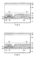
- FIG. 1 The cross-sectional view of the pixel of the flat panel X-ray detector according to this embodiment is shown in FIG. 1. Next, the manufacturing steps of the flat panel X-ray detector according to this embodiment will be explained with reference to FIG. 1.
- either a single layer of film formed of MoTa, Ta, TaN, Al, Al alloy or MoW, or a double layer consisting of Ta and TaNx is deposited to a thickness of about 300 nm on the surface of a glass substrate 101, and the deposited layer is patterned by means of etching to form a gate electrode 102 of a switching TFT 402, a scanning line (not shown), an electrode 102a of a storage capacitance 404, and a storage capacitance line (not shown).
- SiOx is deposited to a thickness of about 300 nm and SiNx is deposited to a thickness of about 50 nm, thereby forming a laminated insulating film 103.
- an undoped a-Si layer 104 having a thickness of about 100 nm and a stopper 105 consisting of SiNx and having a thickness of about 200 nm are successively deposited.
- the stopper 105 is patterned in conformity with the gate electrode 102, and then, an n + a-Si layer 106 is deposited thereon to a thickness of about 50 nm. Thereafter, the a-Si layer 104 and the n + a-Si layer 106 are etched to form an island consisting of a-Si in conformity with the configuration of transistor.
- Part of the insulating film 103 which corresponds to the contact portions inside of the pixel area and outside of the pixel area is etched away to form contact holes. Then, by means of sputtering, a layer of Mo having a thickness of about 50 nm, a layer of Al having a thickness of about 350 nm and another layer of Mo having a thickness of about 20 nm to 50 nm are laminated thereon to form an auxiliary electrode 502, a signal line 408, the source/drain of TFT, and other wirings.
- a layer of SiNx having a thickness of about 200 nm, and a layer of acrylic resin (HRC: trade name, Nippon Gosei Rubber Co., Ltd.) having a thickness of about 1 to 5 ⁇ m, preferably about 3.5 ⁇ m are deposited to form a protective film 107.
- HRC trade name, Nippon Gosei Rubber Co., Ltd.
- BCB may be employed in place of the HRC.
- an ITO film is formed as a metal for the pixel electrode.
- This ITO film is formed to a thickness of 1000 angstroms by means of sputtering method using ITO as a target.
- a pixel electrode pattern is formed on this ITO film and employed as a mask to perform the patterning of the ITO film by wet etching. Thereafter, the photoresist is removed to form a pixel electrode 503.
- a p-type SnI 2 layer 210a is formed on the pixel electrode 503 to a thickness of 1 to 50 ⁇ m, more preferably 10 ⁇ m.
- a high resistance SnI 2 layer 210 is formed on the p-type SnI 2 layer 210a to a thickness of about 100 ⁇ m to 1000 ⁇ m, more preferably 300 ⁇ m.
- an n-type SnI 2 layer 210b is formed on the SnI 2 layer 210 to a thickness of 1 to 50 ⁇ m, more preferably 10 ⁇ m at a temperature of 200°C. It is possible, in this manner, to form a laminate of SnI 2 layers 210a, 210 and 210b acting as an X-ray-charge conversion film of high quality and of hexagonal crystal structure having an orientation of (001).
- a layer of Cr having a thickness of 200 nm is formed, without the accompaniment of patterning step, on the surface of the SnI 2 layer 210 to form an upper electrode 212.
- the p-type SnI 2 layer 210a and the n-type SnI 2 layer 210b which are disposed over and below the high resistance SnI 2 layer 210, they are not necessarily be disposed concurrently, but one of them may be omitted.
- the SnI 2 layer 210 may be omitted and only the p-type SnI 2 layer 210a and the n-type SnI 2 layer 210b may be formed instead.
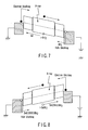
- the band structure of a laminate structure of SnI 2 layers 210a, 210 and 210b as a X-ray-charge conversion film is shown in FIG. 6.
- peripheral driving circuits are mounted on the substrate of the TFT array X-ray-charge conversion film that has been fabricated as described above to thereby accomplish the manufacture of a flat panel X-ray detector.
- the detection of X-ray images was performed by making use of this flat panel X-ray detector, excellent effects were recognized, i.e. it was possible to minimize residual images and to improve the resolution of images as compared with the flat panel X-ray detector which was manufactured by forming, on the pixel electrodes thereof, an X-ray-charge conversion film where the lattice constants of the films are not aligned with one another.
- FIG. 2 The cross-sectional view of the pixel of the flat panel X-ray detector according to this embodiment is shown in FIG. 2. Next, the manufacturing steps of the flat panel X-ray detector according to this embodiment will be explained with reference to FIG. 2.
- an electrode 212 formed of Zr 2 N of (110) azimuth of hexagonal crystal structure is deposited to a thickness of 1000 angstroms on the surface of a glass substrate 901.
- an ion plating or sputtering method is employed and a minus bias is applied onto the substrate, thereby making it possible to control the direction of the orientation of the Zr 2 N.
- a p-type PbI 2 layer 220a is formed on the electrode 212 to a thickness of 1 to 50 ⁇ m, more preferably 10 ⁇ m.
- a high resistance PbI 2 layer 220 is formed on the p-type PbI 2 layer 220a to a thickness of about 100 ⁇ m to 1000 ⁇ m, more preferably 300 ⁇ m.
- an n-type PbI 2 layer 220b is formed on the PbI 2 layer 220 to a thickness of 1 to 50 ⁇ m, more preferably 10 ⁇ m at a temperature of 250°C. It is possible, in this manner, to form a laminate of PbI 2 layers 220a, 220 and 220b, which is excellent in quality and of hexagonal crystal structure having an orientation of (001).
- a lower electrode 213 is formed on this laminate of PbI 2 layers 220a, 220 and 220b. Then, an organic conductive film is coated on this lower electrode 213 and patterned by way of exposure and development in conformity with the pitch of pixels of a TFT array substrate which has been fabricated in the same manner as the above first embodiment, thus forming a connecting electrode column 214.
- the substrate manufactured in this manner is connected with the ITO pixel electrode 503 of the TFT array substrate which has been fabricated in the same manner as the above first embodiment to accomplish the array of the X-ray-charge conversion film.
- the p-type PbI 2 layer 220a and the n-type PbI 2 layer 220b which are disposed over and below the high resistance PbI 2 layer 220, they are not necessarily be disposed concurrently, but one of them may be omitted.
- the PbI 2 layer 220 may be omitted and only the p-type PbI 2 layer 220a and the n-type PbI 2 layer 220b may be formed instead.
- peripheral driving circuits are mounted on the substrate of the TFT array X-ray sensitive film substrate that has fabricated as described above to thereby accomplish the manufacture of a flat panel X-ray detector.
- the detection of X-ray images was performed by making use of this flat panel X-ray detector, excellent effects were recognized, i.e. it was possible to minimize residual image, to improve the resolution of image and to decrease the dark current as compared with the flat panel X-ray detector which was manufactured by forming, on the pixel electrodes thereof, an X-ray-charge conversion film where the lattice constants of the films are not aligned with one another.
- FIG. 3 The cross-sectional view of the pixel of the flat panel X-ray detector according to this embodiment is shown in FIG. 3. Next, the manufacturing steps of the flat panel X-ray detector according to this embodiment will be explained with reference to FIG. 3.
- a TFT array is fabricated on a glass substrate 101 in the same manner as described in the aforementioned first embodiment.
- a V 2 N film is formed as a metal for the pixel electrode to a thickness of 1000 angstroms by means of sputtering method using V 2 N as a target.
- This V 2 N film may be formed by means of sputtering method using a V 2 N target in an Ar atmosphere to which N 2 is added.
- a photoresist pattern is formed on this V 2 N film in conformity with the configuration of the pixel electrodes. Thereafter, by making use of this resist as a mask, the patterning of the V 2 N film is performed by way of RIE using a fluorine-based gas such as CF 4 , etc. Thereafter, the resist is removed to form a pixel electrode 503.
- V 2 N is excellent in corrosion resistance, it is also highly resistive to iodides. Further, since V 2 N is excellent in lattice alignment with a metal iodide, it is suited for use as a lower electrode of the X-ray-charge conversion film.
- a high resistance InI layer 230 is formed on the pixel electrode 503 to a thickness of about 50 ⁇ m.
- a high resistance SnI 2 layer 240 is formed on the InI layer 230 to a thickness of about 100 ⁇ m to 1000 ⁇ m, more preferably 300 ⁇ m at a temperature of 150°C.
- a high resistance BiI 3 layer 250 is formed on the SnI 2 layer 240 to a thickness of 50 ⁇ m.
- a layer of Cr having a thickness of 200 nm is formed, without the accompaniment of patterning step, on the surface of the BiI 3 layer 250 to form an upper electrode 212.
- the band structure of a laminate of InI layer 230/SnI 2 layer 240/BiI 3 layer 250 as a X-ray-charge conversion film is shown in FIG. 7.
- barriers becomes higher in the structure of the flat panel X-ray detector according to this embodiment
- peripheral driving circuits are mounted on the substrate of the TFT array X-ray sensitive film substrate that has fabricated as described above to thereby accomplish the manufacture of a flat panel X-ray detector.
- excellent effects were recognized, i.e. it was possible to minimize residual images and to improve the resolution of images as compared with the flat panel X-ray detector which was manufactured by forming, on the pixel electrodes thereof, an X-ray-charge conversion film where the lattice constants of the films are not aligned with one another.
- Furthermore, owing to excellent blocking effect of dark current it was also recognized very excellent effects that the generation of dark current can be minimized and even faint signals can be detected. In this case, InI 3 can be used instead of InI, because these characteristics are similar.
- FIG. 4 The cross-sectional view of the pixel of the flat panel X-ray detector according to this embodiment is shown in FIG. 4. Next, the manufacturing steps of the flat panel X-ray detector according to this embodiment will be explained with reference to FIG. 4.
- a TFT array is fabricated on a glass substrate 101 in the same manner as described in the aforementioned first embodiment. Then, an ITO film is formed for the pixel electrode to a thickness of 1000 angstroms by means of sputtering method.
- a photoresist pattern is formed on this ITO film in conformity with the configuration of the pixel electrodes. Thereafter, by making use of this resist as a mask, the patterning of the ITO film is performed by way of wet etching. Thereafter, the resist is removed to form a pixel electrode 503.
- ITO is excellent in corrosion resistance, it is also highly resistive to iodides. Also, ITO is usually employed for display electrodes for TFT-LCDs. It is useful to employ the same material and process of TFT-LCD production line for producing TFT arrays for flat panel detectors to decrease the cost for flat panel production.
- a high resistance Sn 0.5 In 0.5 Br 2 layer 260 is formed on the pixel electrode 503 to a thickness of about 50 ⁇ m. Since this Sn 0.5 In 0.5 Br 2 is of p-type, it is possible to further improve the aforementioned blocking effect. Then, a high resistance SnBr 2 layer 270 is formed on this Sn 0.5 In 0.5 Br 2 layer 260 to a thickness of about 100 ⁇ m to 1000 ⁇ m, more preferably 300 ⁇ m at a temperature of 200°C.
- Sn 0.5 Bi 0.5 Br 0.5 layer 280 is formed on this SnBr 2 layer 270 to a thickness of 50 ⁇ m. Since this Sn 0.5 Bi 0.5 Br 0.5 is of n-type, it is possible to further improve the aforementioned blocking effect.
- a layer of Cr having a thickness of 200 nm is formed, without the accompaniment of patterning step, on the surface of this Sn 0.5 Bi 0.5 Br 0.5 layer 280 to form an upper electrode 212.
- the band structure of a laminate of Sn 0.5 In 0.5 Br 2 layer 260/SnBr 2 layer 270/Sn 0.5 Bi 0.5 Br 0.5 layer 280 as a X-ray-charge conversion film is shown in FIG. 8.
- peripheral driving circuits are mounted on the substrate of the TFT array X-ray-charge conversion film substrate that has fabricated as described above to thereby accomplish the manufacture of a flat panel X-ray detector.
- excellent effects were recognized, i.e. it was possible to minimize residual images and to improve the resolution of images as compared with the flat panel X-ray detector which was manufactured by forming, on the pixel electrodes thereof, an X-ray-charge conversion film where the lattice constants of the films are not aligned with one another.
- Furthermore, owing to excellent blocking effect of dark current it was also recognized very excellent effects that the generation of dark current can be minimized and even faint signals can be detected.
- the aforementioned mixed crystal of halide is not confined to the composition of Sn 0.5 In 0.5 Br 2 , but may be suitably selected from the composition of Sn x In (1-x) Br 2 wherein x is suitably selected from the range of 0 to 100% so as to obtain desired blocking effects and the properties of the detector.
- This definition is also applicable to any of halides of I, Br and Cl.
- the crystallinity of the upper SnBr 2 layer 270 and Sn 0.5 In 0.5 Br 0.5 layer can be improved due to the excellentness of these upper layers in lattice alignment with the underlying metal halide layer.
- the present invention is not limited to the case of using lattice matched underlayer electrode.
- the improvement of minimizing residual images, improvement of the resolution of images, and decrease in dark current can be obtained by laminating hexagonal lattice matched metal halide photoconductive layers.
- lattice matched metal halide film lamination good junction between the photoconducting metal halide film and metal halide blocking layer and good quality photoconducting film can be obtained.
- the present invention is not confined to these embodiments.
- the X-ray sensitive materials to be employed for forming the X-ray-charge conversion film any kinds of metal halides can be employed.
- the halogen included in each of the layers should desirably be of the same kind.
- the lattice constants of the metal halides can be made almost the same, and at the same time, can be adjusted to have a different band gap. As a result, it is now possible to realize a dark current-blocking effect in an excellent manner without substantially increasing defects of the metal halides.
- the substrate to be employed in the present invention is not confined to the glass substrate but may be of any kinds of material as long as the TFT can be formed thereon.
- the substrate to be employed in the present invention is not confined to the glass substrate but may be of any kinds of material as long as the TFT can be formed thereon.
- a-Si is employed as a semiconductor for forming the TFT
- polysilicon p-Si
- CdSe CdSe
- the TFT is manufactured by making use of p-Si, it would become possible to miniaturize the TFT due to the high mobility of p-Si, thereby making it possible to enlarge the effective area of pixels and to form the peripheral circuits on the same surface of glass substrate, thus resulting in the reduction of manufacturing cost including the cost for the peripheral circuits.
- the structure of the TFT it may be either a top gate type or a back gate type.
- This protective film 107 may not be photosensitive. However, when this protective film 107 is photosensitive, the patterning thereof can be easily performed and hence this protective film 107 should preferably be photosensitive.
- the present invention provides a flat panel X-ray detector which is capable of minimizing residual images, improving the resolution of images, and decreasing in dark current as compared with the flat panel X-ray detector which is manufactured by forming, on the pixel electrodes thereof, an X-ray-charge conversion film where the lattice constants of the films are not aligned with one another. Furthermore, it is also possible to stabilize the properties of the X-ray-charge conversion film, thereby making it possible to improve the yield in the production of the X-ray-charge conversion film and to provide a high-performance flat panel X-ray detector which is excellent in efficiency and wide in dynamic range.
- the X-ray-charge conversion film is constituted by a laminate structure comprising a plurality of layers differing in band gap one another, it would become possible to realize an excellent blocking effect against the generation of dark current, thus making it possible to provide a flat panel X-ray detector provided with such excellent properties that it is capable of extremely minimizing the generation of dark current and capable of detecting even a faint signal.
- the X-ray-charge conversion film is formed of a laminate film consisting of a plurality of metal halide films differing in band gap and laminated along the c-axis of hexagonal crystal structure.
- the X-ray-charge conversion film is not necessarily a laminate film, and may be a mono-layer film provided that at least one of a pair of electrodes contacting with the mono-layer film is formed of a conductive film which is lattice-matched with the metal halide film. Namely, even if the X-ray-charge conversion film is constituted by a mono-layer film in such a manner as described above, the effects of the X-ray-charge conversion film to minimize the generation of dark current can be retained.
- FIGS. 1 and 2 Specific examples of the flat panel X-ray detector having an X-ray-charge conversion film of aforementioned constructions can be estimated from FIGS. 1 and 2, i.e. in the flat panel X-ray detector of the first embodiment which is shown in FIG. 1, the p-type SnI 2 layer 210a and the n-type SnI 2 layer 210b are both deleted therefrom; and in the flat panel X-ray detector of the second embodiment which is shown in FIG. 2, the p-type PbI 2 layer 220a and the n-type PbI 2 layer 220b are both deleted therefrom.
Landscapes
- Physics & Mathematics (AREA)
- Engineering & Computer Science (AREA)
- Power Engineering (AREA)
- High Energy & Nuclear Physics (AREA)
- Health & Medical Sciences (AREA)
- Toxicology (AREA)
- Electromagnetism (AREA)
- Condensed Matter Physics & Semiconductors (AREA)
- General Physics & Mathematics (AREA)
- General Engineering & Computer Science (AREA)
- Computer Hardware Design (AREA)
- Microelectronics & Electronic Packaging (AREA)
- Measurement Of Radiation (AREA)
- Solid State Image Pick-Up Elements (AREA)
- Light Receiving Elements (AREA)
Abstract
Description
- This invention relates to a flat panel X-ray detector which is adapted to be used in a medical X-ray diagnostic device.
- In recent years, there is an increasing trend in the medical field to store the medical data of patients in the form of data base. The reason for this trend is due to the facts that since patients often desire to utilize a plurality of medical facilities for the medical treatment of the same disease, one of the medical facilities which is going to examine such patients may require to know the data that has been already obtained by other medical facilities, in order to enable the medical facilities to perform more appropriate medical treatments on such patients.
- There is also a strong demand to store the image data of X-ray photographing in the form of data base, and therefore, it is desired to digitize the images produced by X-ray photography. In the conventional medical X-ray diagnostic device, X-ray images are taken by making use of a silver film. If it is desired to digitize such X-ray images, an operation of reading the images that have been photographed and developed on the film is required by making use of a scanner and the like, thus necessitating a troublesome and time-consuming operation.
- Recently, there has been developed an image intensifier TV (II-TV) system which is capable of directly digitizing the X-ray images by making use of a CCD camera of about 1 inch and a large scale vacuum tube provided with a photoelectric film, accelerating electrodes and a fluorescent film. However, this II-TV system is accompanied with a problem that in the case of diagnosing lungs for example, an optical apparatus for achieving the convergence of light for taking a picture of as large an area as 40 cm x 40 cm is required, thereby necessitating a large scale apparatus. Further, because of the distortion of image caused due to the deflection of electron beam resulting from the earth's magnetism, or because of the deterioration of resolution resulting from a series of electronic and optical systems such as a fluorescent film, a CCD, etc., the quality of image is caused to deteriorate.
- There is also proposed, as a new system for overcoming the problems accompanied with the aforementioned conventional two systems, an X-ray image pickup apparatus using an amorphous silicone thin film transistor (a-Si TFT) (hereinafter referred to as a flat panel X-ray detector) (for example, US Patent No. 4,689,487).
- According to this flat panel X-ray detector, the pixels thereof are all constituted by the a-Si TFT, a photoelectric conversion film and pixel capacitance, and these pixels are arranged in the form of an array where hundreds or thousands of pixels are aligned along vertical and horizontal lines (hereinafter referred to as TFT array).
- In this flat panel X-ray detector, a bias voltage from a power source is applied to the photoelectric conversion film, and the a-Si TFT is connected with a signal line and with a scanning line and controlled to turn ON/OFF by means of a scanning line driving circuit. The terminal of the signal line is connected, via a change-over switch, with a signal-detecting amplifier.
- When a beam of light is irradiated to the detector, an electric current is permitted to flow through the photoelectric conversion film so as to enable electric charge to be stored in the pixel capacitance. The scanning line is designed to be driven by means of the scanning line driving circuit, so that when all TFTs connected with a single scanning line are turned ON, the electric charge stored as mentioned above is transmitted, via the signal line, to the amplifier side. In every pixel, electric charge is inputted into the amplifier by making use of the change-over switch and then converted sequentially into a signal so as to enable it to be displayed on a CRT, etc. In this case, depending on the magnitude of the light entering into the pixel, the magnitude of electric charge is caused to change, thereby causing the output amplitude of the amplifier to change.
- According to this system, X-ray images can be directly turned into digital images by A/D-converting the output signals of the amplifier. Further, since the pixel region thereof is formed of the same structure as that of a thin film transistor liquid crystal display (TFT-LCD) which is commonly employed in a note-type personal computer, a display which is thin and large in picture plane can be easily manufactured.
- These conventional systems explained above are all related to a flat panel X-ray detector of indirect conversion system wherein the incident X-ray is converted by means of a fluorescent substance, etc. into visible light, which is then converted into electric charge by means of the photoelectric conversion film of each of the pixels.
- Apart from these conventional systems, there is also known a flat panel X-ray detector of direct conversion system wherein the X-ray entering into the pixels is directly converted into electric charge. This flat panel X-ray detector conversion system differs from that of indirect conversion system in the respect that an X-ray is directly converted by means of the photoelectric conversion film into electric charge, which is then stored in the pixel capacitance. Namely, this flat panel X-ray detector of direct conversion system is almost identical in structure with the flat panel X-ray detector of indirect conversion system except that the fluorescent substance is not provided therewith.
- This flat panel X-ray detector of direct conversion system is constructed such that a capacitor (Cst) consisting of a laminate structure comprising a capacitor electrode, an insulating layer and an auxiliary electrode, a switching TFT connected with the capacitor, and a protective TFT are disposed on the surface of a glass substrate. Each of these components is covered with a protecting film having a contact hole disposed over the auxiliary electrode. On this protecting film, there are successively superimposed a pixel electrode (which is connected via the contact hole with the auxiliary electrode), an X-ray-charge conversion film, and a common electrode (upper electrode). The pixels constructed as described above are arranged in a form of array.
- When X-ray is irradiated to the detector, the X-ray is converted by means of the X-ray-charge conversion film into electric charge which is then accelerated by an electric field applied between the common electrode and the pixel electrode and stored in the capacitor. The switching TFT is driven through the scanning line so as to transfer the electric charge that has been stored in the capacitor to the signal line. The function of the protective TFT is to release electric charge whenever an excessive electric charge happens to be generated.
- It is required that the signal charge generated from the X-ray is enabled to immediately reach the pixel electrode and stored in the pixel capacitance. If the signal charge is permitted to remain inside the X-ray-charge conversion film, it would lead to the generation of defective images such as residual images where the previous image patterns are left behind or the deterioration of resolution. Most of these defective images are caused to generate due to the signal charge that has been left remained in the X-ray-charge conversion film and acts to badly affect the traveling of the signal charge that has been newly generated by the X-ray. Further, there is another problem that when the X-ray-charge conversion film is accompanied with a large number of defects, electric current passing through such defects is generated, thereby increasing the dark current.
- It is conventionally known to construct the X-ray-charge conversion film by making use of PbI2 which is excellent in properties and is expected to be very useful as a material for forming the X-ray-charge conversion film. As a matter of fact however, since this PbI2 is poor in crystallinity especially when it is formed into a thin film, the employment of this PbI2 is also accompanied with the same problems as mentioned above, i.e. residual images, the deterioration of resolution, the generation in considerable degree of dark current, etc. Therefore, up to date, no one has succeeded to manufacture the X-ray-charge conversion film which is excellent in properties (see R.A. Street et al., SPIE Vol. 3659, P. 36,1999).
- It is imperative to improve the quality of the X-ray-charge conversion film in order to overcome the generation of aforementioned defective images. According to the prior art however, since a polycrystalline X-ray-charge conversion film which is not so good in quality is deposited on the surface of the underlying substrate in general, a large number of grain boundaries and traps are caused to exist in the film near the interface between the film and the substrate, thereby making it impossible to avoid the generation of residual images and the deterioration of the resolution of images. Furthermore, since a large magnitude of dark current is generated in the case of such a defective film as mentioned above, it is very difficult to perform the detection of images under a faint X-ray dose.
- As explained above, as long as the conventional photosensitive films are to be employed for the manufacture of the flat panel X-ray detector, it has been very difficult to form the X-ray-charge conversion film which is excellent in quality. Therefore, it has been very difficult to overcome the generation of residual images, as the deterioration of the resolution of images, and especially the generation of large dark current.
- An object of the present invention is to provide a flat panel X-ray detector which is capable of improving image defects such as the generation of residual images and the deterioration of resolution of images, and capable of overcoming the difficulties of detecting images by making use of faint X-ray that may be attributed to an increased generation of dark current.
- According to an aspect of the present invention, there is provided a flat panel X-ray detector which comprises: an X-ray-charge conversion film converting incident X-rays into electric charges; and a pair of electrodes disposed in contact with both surfaces of the X-ray-charge conversion film; wherein the X-ray-charge conversion film has a laminate structure including a plurality of metal halide films laminated along direction of c-axis of hexagonal crystal structure and differing in band gap from one another, and halogen atoms contained in the plurality of metal halide films are of the same kind among them.
- According to another aspect of the present invention, there is provided a flat panel X-ray detector which comprises: an X-ray-charge conversion film converting incident X-rays into electric charge; pixel electrodes formed on the X-ray-charge conversion film to correspond with each of pixels which are arranged in a form of array; switching elements each electrically connected with each of the pixel electrodes;
signal lines each electrically connected with the switching element of each row; scanning lines each electrically connected with the switching element of each column; and
a common electrode which is disposed on one of the surfaces of the X-ray-charge conversion film, which is opposite to the surface where the pixel electrodes of the X-ray-charge conversion film are disposed; wherein the X-ray-charge conversion film has a laminate structure comprising a plurality of metal halide films laminated along a direction of c-axis of hexagonal crystal structure and differing in band gap from one another, the halogen atoms of the metal halide films are of the same kind with one another. - This summary of the invention does not necessarily describe all necessary features so that the invention may also be a sub-combination of these described features.
- The invention can be more fully understood from the following detailed description when taken in conjunction with the accompanying drawings, in which:
- FIG. 1 is a cross-sectional view of the flat panel X-ray detector according to a first embodiment of the present invention;
- FIG. 2 is a cross-sectional view of the flat panel X-ray detector according to a second embodiment of the present invention;
- FIG. 3 is a cross-sectional view of the flat panel X-ray detector according to a third embodiment of the present invention;
- FIG. 4 is a cross-sectional view of the flat panel X-ray detector according to a fourth embodiment of the present invention;
- FIG. 5 is a diagram illustrating a state where an SnI2 is lattice-matched with an underlying substrate;
- FIG. 6 is a diagram illustrating the band structure of the X-ray-charge conversion film of the flat panel X-ray detector according to a first embodiment of the present invention;
- FIG. 7 is a diagram illustrating the band structure of the X-ray-charge conversion film of the flat panel X-ray detector according to a third embodiment of the present invention; and
- FIG. 8 is a diagram illustrating the band structure of the X-ray-charge conversion film of the flat panel X-ray detector according to a fourth embodiment of the present invention.
-
- Following are explanation of the flat panel X-ray detector according to one embodiment of the present invention.
- In this flat panel X-ray detector according to one embodiment of the present invention, the X-ray-charge conversion film is formed of a laminate structure comprising a plurality of metal halide films differing in band gap from one another and laminated along the direction of c-axis of hexagonal crystal structure, the halogen atoms in the metal halide films are of the same kind with one another.
- The reason for employing metal halides as an X-ray sensitive material forming the X-ray-charge conversion film resides in the fact that metal halides are excellent in X-ray-charge conversion efficiency. As for specific examples of metal halides, it is preferable to select those having a high X-ray absorption coefficient in order to realize high absorption efficiency of X-ray.
- As for the metal of the metal halides, it is preferable to select from Pb, Hg, Tl, Bi, Cd, In, Sn and Sb, because they have high X-ray absorption coefficient. Among them, Pb, Hg, and Bi, all having very high X-ray absorption coefficient, are more preferable. In view of minimizing the environmental influence of the metal halides, however, it is more preferable not to employ Hg and Pb both giving an influence on environmental safety, but is preferable to select from In, Bi and Sn.
- As for the halogen of the metal halides, it is preferable to select from Cl, Br and I. Among them, I which has high absorption coefficient is most preferable.
- More specifically, the employment of InI, InI3, BiI3 and SnI2 as a metal halide is more preferable than HgI2, PbI2 and CdI2. These materials are basically of hexagonal crystal structure, and the lattice constant are nearly the same between these halides with the same halide and different metals. Since the specific resistance in the direction of c-axis of hexagonal crystal structure is relatively high, when the X-ray-charge conversion film is constructed by making use of these materials of hexagonal crystal structure in the C-axis direction, it is now possible to suppress the generation of dark current at the interface between different kind of metal halide, thereby making it possible to detect faint signals and hence to improve the performance of the X-ray detector.
- Although part of Bi atoms of the hexagonal structure of BiI3, BiBr3, BiCl3, etc. is missing, even if the hexagonal structure is partially deficient in this manner, the effects to be derived from the lattice matching would be almost the same as those where the hexagonal structure is non-deficient. Therefore, by depositing these metal halide films to form a multilayer metal halide films, on the surface of different metal but the same halogen, it is possible to form an X-ray-charge conversion film excellent in quality.
- Also a similar effect can be realized between a metal halide film and a substrate with basically hexagonal structure. These materials are basically of hexagonal crystal structure as exemplified by SnI2 shown in FIG. 5, and the lattice constant thereof is close to the lattice constant of the underlying substrate. Since the specific resistance in the direction of c-axis of hexagonal crystal structure is relatively high, when the X-ray-charge conversion film is constructed by making use of these materials of hexagonal crystal structure, it is now possible to suppress the generation of dark current at the interface between a metal halide and a hexagonal like substrate, thereby making it possible to detect faint signals and hence to improve the performance of the X-ray detector.
- Specific examples of the embodiments of the present invention of the X-ray-charge conversion film that can be preferably employed for fabricating the flat panel X-ray detector will be explained as follows.
- 1. A laminate structure formed of metal halides which are the same in kind with one another but differ in conductivity type from one another: Specific example of this laminate structure includes a laminate consisting of an n-type metal halide film and a p-type metal halide film, such as a laminate of a Bi-doped n-type PbI2 film and an In-doped p-type PbI2 film.Alternatively, example of this laminate structure also includes a laminate consisting of an n-type metal halide film, an i-type metal halide film and a p-type metal halide film, such as a laminate consisting of a Bi-doped n-type PbI2 film, an undoped PbI2 film and an In-doped p-type PbI2 film.
- 2. A laminate structure formed of mixed crystalline metal halides consisting of the same kinds of metal halides but additionally including different kinds of metal elements therein: Specific example of this laminate structure includes a laminate consisting of a PbxByI film, a PbI2 film and a PbxInyI film.
- 3. A laminate structure formed of various kinds of metal halides: Specific example of this laminate structure includes a laminate consisting of a BiI3 film, a PbI2 film and an InI3 film.
-
- Since every films of the aforementioned laminate structure are all formed of a hexagonal crystal structure and all of the halogens included in each film of the laminate structure are the same in kind, the lattice constant of the films of the laminate structure is approximately the same with one another and hence all of the films are laminated along the direction of c-axis. Incidentally, this laminating direction may not necessarily be completely the same as that of c-axis but may be more or less deviated from the direction of c-axis, e.g. by an angle between +5° and -5°.
- As for the thickness of the X-ray-charge conversion film formed of a laminate film, it may be optionally selected as long as it is capable of sufficiently absorbing X-ray. In particular, the thickness of a high resistance semiconductor film may be optionally selected as long as a photo-carrier (electron or hole) is enabled to travel through the high resistance film within a time of about 1/10 of the address time.
- In the flat panel X-ray detector according to one embodiment of the present invention, it is preferable that at least one of a pair of electrodes is formed of a conductive film which can be aligned in lattice matching with metal halide films disposed neighboring thereon.
- As for the underlying substrate for the metal halide film, it may be a bulk form or a thin film. As for the materials for the substrate, any conducting film can be used such as metal, ITO, SnO2 and so on. It is preferable to employ a material whose lattice constant of equivalent hexagonal crystal structure is close to that of the metal halide.
- In the case where halogen of the metal halide is I, it is preferable to employ a material formed of a hexagonal crystal structure having a-axis lattice constant of 4.5 angstroms, a face-centered cubic structure having a-axis lattice constant of 6.45 angstroms or a body-centered cubic structure having a-axis lattice constant of 3.97 angstroms, as for the materials for the substrate.
- In the case where halogen of the metal halide is Br, it is preferable to employ a material formed of a hexagonal crystal structure, a face-centered cubic structure or a body-centered cubic structure having a-axis lattice constant of 3.88 angstroms,
5.49 angstroms or 3.38 angstroms, respectively. In the case where halogen of the metal halide is Cl, it is preferable to employ a material formed of a hexagonal crystal structure, a face-centered cubic structure or a body-centered cubic structure having a-axis lattice constant of 3.44 angstroms, 4.86 angstroms or
2.99 angstroms, respectively. - As for the materials for the substrate, it is preferable to employ a material having a lattice constant which is close to the lattice constant of the ab crystal face of hexagonal crystal structure of the metal halide. Examples of suitable materials for the substrate where the halogen of the metal halide is iodine are shown below together with the lattice constants thereof (numerals in the parenthesis are based on angstrom). Of course, the materials for the substrate are not confined to the following materials but may be selected from other kinds of materials as long as the lattice constant thereof is close to that of the metal halides.
- The aforementioned example of suitable materials for the substrate includes Se(4.36), Te(4.46), HgS(4.15), CdS(4.14), AgI(4.60), Ca(3.98), B2O3(4.325), RbC8(4.98), Co2N(4.6), Cr2N(4.75), CoTa2N2(5.16), FeTa2N2(5.16), TaN(5.19) and V2N(4.91).
- Next, preferable examples of the material for the substrate where the substrate is formed of a face-centered cubic structure are shown below together with the lattice constants thereof (angstroms). As shown in FIG. 5, the (111) plane of the face-centered cubic structure is lattice-matched with the metal halide of hexagonal crystal structure. Namely, such preferable examples of materials include Ni(3.52), Ge(5.65), αSn(6.486), CdSe(6.05), InSb(6.478), AlSb(6.1355), GaSb(6.0955), PbTe(6.46), AgBr(5.77), CdTe(6.48), HgTe(6.46), PbS(5.936) and AgI(6.496).
- Preferable examples of the material for the substrate where the substrate is formed of a body-centered cubic structure are shown below together with the lattice constants thereof (angstroms). As shown in FIG. 5, the (110) plane of the body-centered cubic structure is lattice-matched with the metal halide of hexagonal crystal structure. Namely, such preferable examples of materials include γCa(4.477), Eu(4.606), γSr(4.84), βTh(4.11), βTl(3.874), SnO2(4.21), TiN(4.24), ZrN(4.577), HfN(4.526), VN(4.14), CrN(4.149) and TaN(4.38). In the case of rhombohedron also, the materials should preferably have the similar lattice constant as that of hexagonal crystal structure.
- Since halogen is highly reactive, the underlying substrate should preferably be selected from materials which are excellent in chemical resistance. Among the aforementioned materials, preferable examples in terms of chemical resistance include, in the case of hexagonal crystal structure, CdS(4.14), B2O3(4.325), RbC8(4.98), Co2N(4.6), Cr2N(4.75), CoTa2N2(5.16), FeTa2N2(5.16), TaN(5.19) and V2N(4.91).
- Preferable examples in terms of acid resistance include, in the case of face-centered cubic structure, Ge(5.65), CdSe(6.05), InSb(6.478), AlSb(6.1355), GaSb(6.0955), PbTe(6.46), CdTe(6.48), HgTe(6.46) and PbS(5.936).
- Preferable examples in terms of chemical resistance include, in the case of body-centered cubic structure, SnO2(4.21), TiN(4.24), ZrN(4.577), HfN(4.526), VN(4.14), CrN(4.149) and TaN(4.38).
- As for the method of forming a film for the underlying substrate, any kind of method such as a sputtering method, a vapor deposition method, an ion plating method, etc. can be employed. In particular, by means of bias voltage, it becomes possible to control the crystal structure as well as the crystal orientation of the film.
- As long as the misalignment of lattice between the underlying substrate and the metal halide can be confined within 10% (between -10% and +10%), it would be possible to form a metal halide film which is excellent in crystallinity on the surface of the underlying substrate. If this misalignment of lattice can be confined to not more than 20%, it is possible to control the crystalline structure as well as the orientation of the metal halide. However, when this misalignment of lattice is increased more than 20%, the orientations of metal halide films would be confused with one another, thereby making it difficult to control the crystalline structure and orientation of the metal halide. Therefore, it would be preferable to confine this misalignment to not higher than 20%. Incidentally, the misalignment of lattice will be represented by a difference in ratio to be obtained by dividing the lattice constant of the metal halide film by the lattice constant of the underlying metal.
- The present invention will be further explained with reference to various examples as follows.
- Following are explanations of the first embodiment of the present invention. The cross-sectional view of the pixel of the flat panel X-ray detector according to this embodiment is shown in FIG. 1. Next, the manufacturing steps of the flat panel X-ray detector according to this embodiment will be explained with reference to FIG. 1.
- First of all, either a single layer of film formed of MoTa, Ta, TaN, Al, Al alloy or MoW, or a double layer consisting of Ta and TaNx is deposited to a thickness of about 300 nm on the surface of a
glass substrate 101, and the deposited layer is patterned by means of etching to form agate electrode 102 of a switching TFT 402, a scanning line (not shown), anelectrode 102a of a storage capacitance 404, and a storage capacitance line (not shown). - Then, by means of plasma CVD, SiOx is deposited to a thickness of about 300 nm and SiNx is deposited to a thickness of about 50 nm, thereby forming a laminated
insulating film 103. Thereafter, an undopeda-Si layer 104 having a thickness of about 100 nm and astopper 105 consisting of SiNx and having a thickness of about 200 nm are successively deposited. - By means of back exposure method, the
stopper 105 is patterned in conformity with thegate electrode 102, and then, an n+a-Si layer 106 is deposited thereon to a thickness of about 50 nm. Thereafter, thea-Si layer 104 and the n+a-Si layer 106 are etched to form an island consisting of a-Si in conformity with the configuration of transistor. - Part of the insulating
film 103 which corresponds to the contact portions inside of the pixel area and outside of the pixel area is etched away to form contact holes. Then, by means of sputtering, a layer of Mo having a thickness of about 50 nm, a layer of Al having a thickness of about 350 nm and another layer of Mo having a thickness of about 20 nm to 50 nm are laminated thereon to form anauxiliary electrode 502, asignal line 408, the source/drain of TFT, and other wirings. - Thereafter, a layer of SiNx having a thickness of about 200 nm, and a layer of acrylic resin (HRC: trade name, Nippon Gosei Rubber Co., Ltd.) having a thickness of about 1 to 5 µm, preferably about 3.5 µm are deposited to form a
protective film 107. In this case, BCB may be employed in place of the HRC. - After a contact hole to the
auxiliary electrode 502 is formed in theprotective film 107, an ITO film is formed as a metal for the pixel electrode. This ITO film is formed to a thickness of 1000 angstroms by means of sputtering method using ITO as a target. - Then, by making use of a photoresist, a pixel electrode pattern is formed on this ITO film and employed as a mask to perform the patterning of the ITO film by wet etching. Thereafter, the photoresist is removed to form a
pixel electrode 503. - Then, by means of vapor deposition, a p-type SnI2 layer 210a is formed on the
pixel electrode 503 to a thickness of 1 to 50 µm, more preferably 10 µm. Thereafter, by means of vapor deposition, a high resistance SnI2 layer 210 is formed on the p-type SnI2 layer 210a to a thickness of about 100 µm to 1000 µm, more preferably 300 µm. Additionally, by means of vapor deposition, an n-type SnI2 layer 210b is formed on the SnI2 layer 210 to a thickness of 1 to 50 µm, more preferably 10 µm at a temperature of 200°C. It is possible, in this manner, to form a laminate of SnI2 layers 210a, 210 and 210b acting as an X-ray-charge conversion film of high quality and of hexagonal crystal structure having an orientation of (001). - A layer of Cr having a thickness of 200 nm is formed, without the accompaniment of patterning step, on the surface of the SnI2 layer 210 to form an
upper electrode 212. Incidentally, with respect to the p-type SnI2 layer 210a and the n-type SnI2 layer 210b which are disposed over and below the high resistance SnI2 layer 210, they are not necessarily be disposed concurrently, but one of them may be omitted. Alternatively, the SnI2 layer 210 may be omitted and only the p-type SnI2 layer 210a and the n-type SnI2 layer 210b may be formed instead. - The band structure of a laminate structure of SnI2 layers 210a, 210 and 210b as a X-ray-charge conversion film is shown in FIG. 6.
- As seen from the band structure diagram shown in FIG. 6, electrons and holes generated in i-type SnI2 layer due to excitation by X rays arrive at an anode and cathode respectively, without any barrier. On the other hand, the number of electrons and holes injected from the cathode and anode respectively, decrease in compared with the case of no p-layer or n-layer, because of the barriers formed by the p-type SnI2 layer and the n-type SnI2 layer. As those electrons and holes from the electrodes, which get over the barriers, produce dark current, the dark current in the flat panel X-ray detector according to this embodiment is low. That is, the structure of the flat panel X-ray detector according to this embodiment is effective in lowering of the dark current.
- Then, peripheral driving circuits are mounted on the substrate of the TFT array X-ray-charge conversion film that has been fabricated as described above to thereby accomplish the manufacture of a flat panel X-ray detector. When the detection of X-ray images was performed by making use of this flat panel X-ray detector, excellent effects were recognized, i.e. it was possible to minimize residual images and to improve the resolution of images as compared with the flat panel X-ray detector which was manufactured by forming, on the pixel electrodes thereof, an X-ray-charge conversion film where the lattice constants of the films are not aligned with one another.
- Following are explanations of the second embodiment of the present invention. The cross-sectional view of the pixel of the flat panel X-ray detector according to this embodiment is shown in FIG. 2. Next, the manufacturing steps of the flat panel X-ray detector according to this embodiment will be explained with reference to FIG. 2.
- First of all, an
electrode 212 formed of Zr2N of (110) azimuth of hexagonal crystal structure is deposited to a thickness of 1000 angstroms on the surface of aglass substrate 901. For the purpose of orientating the Zr2N to the azimuth of (110), an ion plating or sputtering method is employed and a minus bias is applied onto the substrate, thereby making it possible to control the direction of the orientation of the Zr2N. - Then, by means of vapor deposition, a p-type PbI2 layer 220a is formed on the
electrode 212 to a thickness of 1 to 50 µm, more preferably 10 µm. Thereafter, by means of vapor deposition, a high resistance PbI2 layer 220 is formed on the p-type PbI2 layer 220a to a thickness of about 100 µm to 1000 µm, more preferably 300 µm. Additionally, by means of vapor deposition, an n-type PbI2 layer 220b is formed on the PbI2 layer 220 to a thickness of 1 to 50 µm, more preferably 10 µm at a temperature of 250°C. It is possible, in this manner, to form a laminate of PbI2 layers 220a, 220 and 220b, which is excellent in quality and of hexagonal crystal structure having an orientation of (001). - Thereafter, a
lower electrode 213 is formed on this laminate of PbI2 layers 220a, 220 and 220b. Then, an organic conductive film is coated on thislower electrode 213 and patterned by way of exposure and development in conformity with the pitch of pixels of a TFT array substrate which has been fabricated in the same manner as the above first embodiment, thus forming a connectingelectrode column 214. - The substrate manufactured in this manner is connected with the
ITO pixel electrode 503 of the TFT array substrate which has been fabricated in the same manner as the above first embodiment to accomplish the array of the X-ray-charge conversion film. Incidentally, with respect to the p-type PbI2 layer 220a and the n-type PbI2 layer 220b which are disposed over and below the high resistance PbI2 layer 220, they are not necessarily be disposed concurrently, but one of them may be omitted. Alternatively, the PbI2 layer 220 may be omitted and only the p-type PbI2 layer 220a and the n-type PbI2 layer 220b may be formed instead. - Then, peripheral driving circuits are mounted on the substrate of the TFT array X-ray sensitive film substrate that has fabricated as described above to thereby accomplish the manufacture of a flat panel X-ray detector. When the detection of X-ray images was performed by making use of this flat panel X-ray detector, excellent effects were recognized, i.e. it was possible to minimize residual image, to improve the resolution of image and to decrease the dark current as compared with the flat panel X-ray detector which was manufactured by forming, on the pixel electrodes thereof, an X-ray-charge conversion film where the lattice constants of the films are not aligned with one another.
- Following are explanations of the third embodiment of the present invention. The cross-sectional view of the pixel of the flat panel X-ray detector according to this embodiment is shown in FIG. 3. Next, the manufacturing steps of the flat panel X-ray detector according to this embodiment will be explained with reference to FIG. 3.
- First of all, a TFT array is fabricated on a
glass substrate 101 in the same manner as described in the aforementioned first embodiment. Then, a V2N film is formed as a metal for the pixel electrode to a thickness of 1000 angstroms by means of sputtering method using V2N as a target. This V2N film may be formed by means of sputtering method using a V2N target in an Ar atmosphere to which N2 is added. - Then, a photoresist pattern is formed on this V2N film in conformity with the configuration of the pixel electrodes. Thereafter, by making use of this resist as a mask, the patterning of the V2N film is performed by way of RIE using a fluorine-based gas such as CF4, etc. Thereafter, the resist is removed to form a
pixel electrode 503. - Since V2N is excellent in corrosion resistance, it is also highly resistive to iodides. Further, since V2N is excellent in lattice alignment with a metal iodide, it is suited for use as a lower electrode of the X-ray-charge conversion film.
- Then, by means of vapor deposition, a high
resistance InI layer 230 is formed on thepixel electrode 503 to a thickness of about 50 µm. Then, by means of vapor deposition, a high resistance SnI2 layer 240 is formed on theInI layer 230 to a thickness of about 100 µm to 1000 µm, more preferably 300 µm at a temperature of 150°C. Additionally, by means of vapor deposition, a high resistance BiI3 layer 250 is formed on the SnI2 layer 240 to a thickness of 50 µm. - Further, a layer of Cr having a thickness of 200 nm is formed, without the accompaniment of patterning step, on the surface of the BiI3 layer 250 to form an
upper electrode 212. - It is possible, in this manner, to realize the blocking effect of low dark current by forming a laminate of
InI layer 230/SnI2 layer 240/BiI3 layer 250. Since the band gaps of these InI, SnI2 and BiI3 are 2.01 eV, 2.45 eV and 1.73 eV, respectively, these layers are enabled to constitute a band structure which is capable of effectively blocking the hole and the electron. - Moreover, since these InI, SnI2 and BiI3 can be assumed as being a hexagonal crystal structure as mentioned above and are enabled to take values which are very close to a=4.6 and c=7.0, it is possible to minimize the misalignment of lattice and to realize very excellent lattice alignment, thus making it possible to substantially obviate the generation of defects.
- The band structure of a laminate of
InI layer 230/SnI2 layer 240/BiI3 layer 250 as a X-ray-charge conversion film is shown in FIG. 7. - As seen from the band structure view shown in FIG. 7, electrons and holes generated in i-type SnI2 layer due to excitation by X rays arrive at an anode and cathode without any barrier. On the other hand, the number of electrons and holes injected from the cathode and anode respectively, which can get over barriers formed by the InI layer and the BiI3 layer, are smaller. As those electrons and holes, which get over the barriers, produce dark current, the dark current in the flat panel X-ray detector according to this embodiment is low. That is, the structure of the flat panel X-ray detector according to this embodiment is effective in lowering of the dark current.
- Furthermore, as the portion of the SnI2 layer near the InI layer is doped with p-type impurity, InI layer is doped with n-type impurity, the portion of the SnI2 layer near the BiI3 layer is doped with n-type impurity, and the BiI3 layer is doped with p-type impurity, barriers becomes higher in the structure of the flat panel X-ray detector according to this embodiment
- Then, peripheral driving circuits are mounted on the substrate of the TFT array X-ray sensitive film substrate that has fabricated as described above to thereby accomplish the manufacture of a flat panel X-ray detector. When the detection of X-ray images was performed by making use of this flat panel X-ray detector, excellent effects were recognized, i.e. it was possible to minimize residual images and to improve the resolution of images as compared with the flat panel X-ray detector which was manufactured by forming, on the pixel electrodes thereof, an X-ray-charge conversion film where the lattice constants of the films are not aligned with one another. Furthermore, owing to excellent blocking effect of dark current, it was also recognized very excellent effects that the generation of dark current can be minimized and even faint signals can be detected. In this case, InI3 can be used instead of InI, because these characteristics are similar.
- Following are explanations of the fourth embodiment of the present invention. The cross-sectional view of the pixel of the flat panel X-ray detector according to this embodiment is shown in FIG. 4. Next, the manufacturing steps of the flat panel X-ray detector according to this embodiment will be explained with reference to FIG. 4.
- First of all, a TFT array is fabricated on a
glass substrate 101 in the same manner as described in the aforementioned first embodiment. Then, an ITO film is formed for the pixel electrode to a thickness of 1000 angstroms by means of sputtering method. - Then, a photoresist pattern is formed on this ITO film in conformity with the configuration of the pixel electrodes. Thereafter, by making use of this resist as a mask, the patterning of the ITO film is performed by way of wet etching. Thereafter, the resist is removed to form a
pixel electrode 503. - Since ITO is excellent in corrosion resistance, it is also highly resistive to iodides. Also, ITO is usually employed for display electrodes for TFT-LCDs. It is useful to employ the same material and process of TFT-LCD production line for producing TFT arrays for flat panel detectors to decrease the cost for flat panel production.
- Then, by means of vapor deposition, a high resistance Sn0.5In0.5Br2 layer 260 is formed on the
pixel electrode 503 to a thickness of about 50 µm. Since this Sn0.5In0.5Br2 is of p-type, it is possible to further improve the aforementioned blocking effect. Then, a high resistance SnBr2 layer 270 is formed on this Sn0.5In0.5Br2 layer 260 to a thickness of about 100 µm to 1000 µm, more preferably 300 µm at a temperature of 200°C. - Then, by means of vapor deposition, a high resistance Sn0.5Bi0.5Br0.5 layer 280 is formed on this SnBr2 layer 270 to a thickness of 50 µm. Since this Sn0.5Bi0.5Br0.5 is of n-type, it is possible to further improve the aforementioned blocking effect.
- Further, a layer of Cr having a thickness of 200 nm is formed, without the accompaniment of patterning step, on the surface of this Sn0.5Bi0.5Br0.5 layer 280 to form an
upper electrode 212. - It is possible, in this manner, to realize the blocking effect of low dark current by forming a laminate of Sn0.5In0.5Br2 layer 260/SnBr2 layer 270/Sn0.5Bi0.5Br0.5 layer 280. Since the band gap of the SnBr2 is larger than that of Sn0.5Bi0.5Br0.5 and Sn0.5In0.5Br2, these layers are enabled to constitute a band structure which is capable of effectively blocking the hole and the electron.
- Moreover, since these Sn0.5In0.5Br2, SnBr2 and Sn0.5Bi0.5Br0.5 can be assumed as being a hexagonal crystal structure as mentioned above and are enabled to take values which are very close to a=3.9 and c=5.5, it is possible to minimize the misalignment of lattice and to realize very excellent lattice alignment, thus making it possible to substantially obviate the generation of defects.
- The band structure of a laminate of Sn0.5In0.5Br2 layer 260/SnBr2 layer 270/Sn0.5Bi0.5Br0.5 layer 280 as a X-ray-charge conversion film is shown in FIG. 8.
- As seen from the band structure view shown in FIG. 8, electrons and holes generated in the SnBr2 layer due to excitation by X rays arrive at an anode and cathode, respectively, without any barrier. On the other hand, the number of electrons and holes injected from the cathode and anode, respectively, which can get over barriers formed by the Sn0.5In0.5Br2 layer and the Sn0.5Bi0.5Br0.5 layer, are decreased. As those electrons and holes from the electrodes, which get over the barriers, produce dark current, the dark current in the flat panel X-ray detector according to this embodiment is low. That is, the structure of the flat panel X-ray detector according to this embodiment is effective in lowering of the dark current.
- Furthermore, as the portion of the SnBr2 layer near the Sn0.5In0.5Br2 layer is doped with p-type impurity, and the portion of the SnBr2 layer near the Sn0.5Bi0.5Br0.5 layer is doped with n-type impurity, barriers becomes higher in the structure of the flat panel X-ray detector according to this embodiment
- Then, peripheral driving circuits are mounted on the substrate of the TFT array X-ray-charge conversion film substrate that has fabricated as described above to thereby accomplish the manufacture of a flat panel X-ray detector. When the detection of X-ray images was performed by making use of this flat panel X-ray detector, excellent effects were recognized, i.e. it was possible to minimize residual images and to improve the resolution of images as compared with the flat panel X-ray detector which was manufactured by forming, on the pixel electrodes thereof, an X-ray-charge conversion film where the lattice constants of the films are not aligned with one another. Furthermore, owing to excellent blocking effect of dark current, it was also recognized very excellent effects that the generation of dark current can be minimized and even faint signals can be detected.
- Incidentally, the aforementioned mixed crystal of halide is not confined to the composition of Sn0.5In0.5Br2, but may be suitably selected from the composition of SnxIn(1-x)Br2 wherein x is suitably selected from the range of 0 to 100% so as to obtain desired blocking effects and the properties of the detector. This definition is also applicable to any of halides of I, Br and Cl.
- The effects of using the same halogen (I, Br or Cl) in combination with different kinds of metals as shown in the third and fourth embodiments can be derived individually or independently without necessitating the employment of a substrate which is lattice-matched with the metal halides. The reason for this can be attributed to the fact that due to the effect of aligning with an underlying metal halide layer, the crystallinity of upper halide layer can be improved. For example, when the Sn0.5In0.5Br2 layer 260 is vapor-deposited on the surface of a metal layer which is not aligned in lattice with the
layer 260 and then, an SnBr2 layer 270 and another SnBr2 layer 270 are successively deposited, the crystallinity of the upper SnBr2 layer 270 and Sn0.5In0.5Br0.5 layer can be improved due to the excellentness of these upper layers in lattice alignment with the underlying metal halide layer. - The present invention is not limited to the case of using lattice matched underlayer electrode. The improvement of minimizing residual images, improvement of the resolution of images, and decrease in dark current can be obtained by laminating hexagonal lattice matched metal halide photoconductive layers. By using lattice matched metal halide film lamination, good junction between the photoconducting metal halide film and metal halide blocking layer and good quality photoconducting film can be obtained.
- Various embodiments of the present invention have been explained above, the present invention is not confined to these embodiments. For example, as for the X-ray sensitive materials to be employed for forming the X-ray-charge conversion film, any kinds of metal halides can be employed. Incidentally, when the X-ray-charge conversion film is constituted by a plurality of layers, the halogen included in each of the layers should desirably be of the same kind. As long as the halogen included in these layers is the same in kind, the lattice constants of the metal halides can be made almost the same, and at the same time, can be adjusted to have a different band gap. As a result, it is now possible to realize a dark current-blocking effect in an excellent manner without substantially increasing defects of the metal halides.
- In the foregoing embodiments, although a glass substrate is employed as a substrate for forming a TFT thereon, the substrate to be employed in the present invention is not confined to the glass substrate but may be of any kinds of material as long as the TFT can be formed thereon. For example, it is possible to employ a heat resistant plastic, in which case the resultant flat panel X-ray detector can be provided with plastic property as a whole.
- In the foregoing embodiments, although a-Si is employed as a semiconductor for forming the TFT, it is also possible to employ polysilicon (p-Si), CdSe, etc. When the TFT is manufactured by making use of p-Si, it would become possible to miniaturize the TFT due to the high mobility of p-Si, thereby making it possible to enlarge the effective area of pixels and to form the peripheral circuits on the same surface of glass substrate, thus resulting in the reduction of manufacturing cost including the cost for the peripheral circuits.
- As for the structure of the TFT, it may be either a top gate type or a back gate type.
- With respect to the
protective film 107 for covering the TFT, it is possible to employ inorganic materials such as SiNx or SiO2 or organic materials such as polyimides (ε=about 3.3; pressure resistance: about 300 V/mm), benzocyclobutene (ε=about 2.7; pressure resistance: about 400 V/mm), acrylic photosensitive resin (HRC (trademark); JSR Co., Ltd.) (ε=about 3.2), black resist, etc. These materials may be laminated one another. Since fluorine-based resins are low in relative permittivity) (ε=about 2.1), fluorine-based resins can be also effectively employed as theprotective film 107. Thisprotective film 107 may not be photosensitive. However, when thisprotective film 107 is photosensitive, the patterning thereof can be easily performed and hence thisprotective film 107 should preferably be photosensitive. - As explained above, it is possible according to the present invention to provide a flat panel X-ray detector which is capable of minimizing residual images, improving the resolution of images, and decreasing in dark current as compared with the flat panel X-ray detector which is manufactured by forming, on the pixel electrodes thereof, an X-ray-charge conversion film where the lattice constants of the films are not aligned with one another. Furthermore, it is also possible to stabilize the properties of the X-ray-charge conversion film, thereby making it possible to improve the yield in the production of the X-ray-charge conversion film and to provide a high-performance flat panel X-ray detector which is excellent in efficiency and wide in dynamic range. Especially, when the X-ray-charge conversion film is constituted by a laminate structure comprising a plurality of layers differing in band gap one another, it would become possible to realize an excellent blocking effect against the generation of dark current, thus making it possible to provide a flat panel X-ray detector provided with such excellent properties that it is capable of extremely minimizing the generation of dark current and capable of detecting even a faint signal.
- In the foregoing explanations, the X-ray-charge conversion film is formed of a laminate film consisting of a plurality of metal halide films differing in band gap and laminated along the c-axis of hexagonal crystal structure. However, the X-ray-charge conversion film is not necessarily a laminate film, and may be a mono-layer film provided that at least one of a pair of electrodes contacting with the mono-layer film is formed of a conductive film which is lattice-matched with the metal halide film. Namely, even if the X-ray-charge conversion film is constituted by a mono-layer film in such a manner as described above, the effects of the X-ray-charge conversion film to minimize the generation of dark current can be retained. Specific examples of the flat panel X-ray detector having an X-ray-charge conversion film of aforementioned constructions can be estimated from FIGS. 1 and 2, i.e. in the flat panel X-ray detector of the first embodiment which is shown in FIG. 1, the p-type SnI2 layer 210a and the n-type SnI2 layer 210b are both deleted therefrom; and in the flat panel X-ray detector of the second embodiment which is shown in FIG. 2, the p-type PbI2 layer 220a and the n-type PbI2 layer 220b are both deleted therefrom.
Claims (16)
- A flat panel X-ray detector which comprises:characterized in that said X-ray-charge conversion film (210, 210a, 210b) has a laminate structure including a plurality of metal halide films laminated along direction of c-axis of hexagonal crystal structure and differing in band gap from one another, and halogen atoms contained in said plurality of metal halide films are of the same kind among them.an X-ray-charge conversion film (210, 210a, 210b) converting incident X-rays into electric charges; anda pair of electrodes (212, 503) disposed in contact with both surfaces of said X-ray-charge conversion film,
- A flat panel X-ray detector which comprises:characterized in that said X-ray-charge conversion film(210, 210a, 210b) has a laminate structure comprising a plurality of metal halide films laminated along a direction of c-axis of hexagonal crystal structure and differing in band gap from one another, the halogen atoms of the metal halide films are of the same kind with one another.an X-ray-charge conversion film (210, 210a, 210b) converting incident X-rays into electric charge;pixel electrodes (503) formed on said X-ray-charge conversion film to correspond with each of pixels which are arranged in a form of array;switching elements each electrically connected with each of said pixel electrodes;signal lines (408) each electrically connected with said switching element of each row;scanning lines each electrically connected with said switching element of each column; anda common electrode (212) which is disposed on one of the surfaces of said X-ray-charge conversion film, which is opposite to the surface where said pixel electrodes(503) of said X-ray-charge conversion film(210, 210a, 210b) are disposed;
- The flat panel X-ray detector according to claim 1 or 2, characterized in that at least one of said electrodes (212, 503) is a conductive film which is lattice-matched with said metal halide film disposed neighboring thereon.
- The flat panel X-ray detector according to claim 1 or 2, characterized in that said metal halide film comprises at least one metal halide selected from the group consisting of metal iodide, metal bromide and metal chloride, said metal being selected from the group consisting of Pb, Hg, Sn, Bi, In, Tl, and Cd.
- The flat panel X-ray detector according to claim 1 or 2, characterized in that said metal halide film comprises at least one metal halide selected from the group consisting of PbI2, HgI2, SnI2, BiI3, InI, InI3, Cd I2, and TlI.
- The flat panel X-ray detector according to claim 1 or 2, characterized in that said metal halide film comprises at least one metal halide selected from the group consisting of PbI2, HgI2, SnI2, BiI3, InI and InI3; said electrodes comprises a hexagonal crystal structure having a-axis lattice constant of 4.5 angstroms, a face-centered cubic structure having a-axis lattice constant of 6.45 angstroms or a body-centered cubic structure having a-axis lattice constant of 4.27 angstroms; and lattice mismatching between at least one of said electrodes and said metal halide film disposed neighboring thereon is 20% or less.
- The flat panel X-ray detector according to claim 1 or 2, characterized in that said plurality of metal halide films comprise metal halides which are the same in kind with one another but differ in conductivity type from one another.
- The flat panel X-ray detector according to claim 7, characterized in that said plurality of metal halide films comprise an n-type metal halide film and a p-type metal halide film.
- The flat panel X-ray detector according to claim 8, characterized in that said plurality of metal halide films comprise a Bi-doped n-type PbI2 film and an In-doped p-type PbI2 film.
- The flat panel X-ray detector according to claim 7, characterized in that said plurality of metal halide films comprise an n-type metal halide film, an i-type metal halide film and a p-type metal halide film.
- The flat panel X-ray detector according to claim 10, characterized in that said plurality of metal halide films comprise a Bi-doped n-type PbI2 film, an undoped PbI2 film and an In-doped p-type PbI2 film.
- The flat panel X-ray detector according to claim 1 or 2, characterized in that said plurality of metal halide films comprise mixed crystalline metal halides which are the same in kind with one another but additionally contain different kinds of metal elements therein.
- The flat panel X-ray detector according to claim 12, characterized in that said plurality of metal halide films comprise a PbxByI film, a PbI2 film and a PbxInyI film.
- The flat panel X-ray detector according to claim 1 or 2, characterized in that said plurality of metal halide films comprise various kinds of metal halides.
- The flat panel X-ray detector according to claim 14, characterized in that said plurality of metal halide films comprise a BiI3 film, a PbI2 film and an InI3 film.
- The flat panel X-ray detector according to claim 1 or 2, characterized in that at least one of said electrodes (212, 503) comprise a hexagonal crystal structure having a-axis which is approximately equivalent to (0001), a face-centered cubic structure having a-axis which is approximately equivalent to (111) or a body-centered cubic structure having a-axis which is approximately equivalent to (110).
Applications Claiming Priority (2)
| Application Number | Priority Date | Filing Date | Title |
|---|---|---|---|
| JP2002357121A JP4153783B2 (en) | 2002-12-09 | 2002-12-09 | X-ray flat panel detector |
| JP2002357121 | 2002-12-09 |
Publications (2)
| Publication Number | Publication Date |
|---|---|
| EP1429156A1 true EP1429156A1 (en) | 2004-06-16 |
| EP1429156B1 EP1429156B1 (en) | 2006-07-26 |
Family
ID=32322065
Family Applications (1)
| Application Number | Title | Priority Date | Filing Date |
|---|---|---|---|
| EP03028109A Expired - Lifetime EP1429156B1 (en) | 2002-12-09 | 2003-12-05 | Flat panel X-ray detector |
Country Status (4)
| Country | Link |
|---|---|
| US (1) | US7115878B2 (en) |
| EP (1) | EP1429156B1 (en) |
| JP (1) | JP4153783B2 (en) |
| DE (1) | DE60307028T2 (en) |
Cited By (2)
| Publication number | Priority date | Publication date | Assignee | Title |
|---|---|---|---|---|
| US7276706B2 (en) * | 2004-05-12 | 2007-10-02 | Kabushiki Kaisha Toshiba | Radiation detector |
| DE102011003454A1 (en) * | 2011-02-01 | 2012-08-02 | Siemens Aktiengesellschaft | Direct radiation converter, radiation detector, medical device and method for generating a direct radiation converter |
Families Citing this family (14)
| Publication number | Priority date | Publication date | Assignee | Title |
|---|---|---|---|---|
| US20050056829A1 (en) * | 2003-09-17 | 2005-03-17 | Green Michael C. | Reducing dark current of photoconductor using heterojunction that maintains high x-ray sensitivity |
| US7126128B2 (en) * | 2004-02-13 | 2006-10-24 | Kabushiki Kaisha Toshiba | Flat panel x-ray detector |
| JP4653579B2 (en) * | 2005-07-13 | 2011-03-16 | 株式会社東芝 | X-ray flat panel detector |
| DE102005060795A1 (en) * | 2005-12-16 | 2007-07-12 | Siemens Ag | Flat panel detector |
| DE102005060794B3 (en) * | 2005-12-16 | 2007-06-14 | Siemens Ag | Flat panel detector |
| US8232531B2 (en) * | 2007-03-29 | 2012-07-31 | Varian Medical Systems, Inc. | Corrosion barrier layer for photoconductive X-ray imagers |
| JP2015061041A (en) * | 2013-09-20 | 2015-03-30 | 株式会社東芝 | Radiation detector and radiation detection device |
| KR102306612B1 (en) | 2014-01-31 | 2021-09-29 | 램 리써치 코포레이션 | Vacuum-integrated hardmask processes and apparatus |
| US10712454B2 (en) | 2014-07-25 | 2020-07-14 | General Electric Company | X-ray detectors supported on a substrate having a metal barrier |
| US9513380B2 (en) | 2014-07-25 | 2016-12-06 | General Electric Company | X-ray detectors supported on a substrate having a surrounding metal barrier |
| US9996004B2 (en) | 2015-11-20 | 2018-06-12 | Lam Research Corporation | EUV photopatterning of vapor-deposited metal oxide-containing hardmasks |
| US10796912B2 (en) | 2017-05-16 | 2020-10-06 | Lam Research Corporation | Eliminating yield impact of stochastics in lithography |
| US11921427B2 (en) | 2018-11-14 | 2024-03-05 | Lam Research Corporation | Methods for making hard masks useful in next-generation lithography |
| US11314168B2 (en) | 2020-01-15 | 2022-04-26 | Lam Research Corporation | Underlayer for photoresist adhesion and dose reduction |
Citations (3)
| Publication number | Priority date | Publication date | Assignee | Title |
|---|---|---|---|---|
| EP1043777A2 (en) * | 1999-03-26 | 2000-10-11 | Kabushiki Kaisha Toshiba | X-ray image detector system |
| EP1120833A2 (en) * | 2000-01-12 | 2001-08-01 | Kabushiki Kaisha Toshiba | Planar x-ray detector |
| US20010010361A1 (en) * | 2000-01-27 | 2001-08-02 | Yoshihiro Izumi | Two-dimensional image detector and fabrication method of the same |
Family Cites Families (4)
| Publication number | Priority date | Publication date | Assignee | Title |
|---|---|---|---|---|
| US4689487A (en) | 1984-09-03 | 1987-08-25 | Kabushiki Kaisha Toshiba | Radiographic image detection apparatus |
| EP1121719A4 (en) * | 1999-07-26 | 2007-08-22 | Edge Medical Devices Ltd | Digital detector for x-ray imaging |
| FI20021255A (en) * | 2002-06-27 | 2003-12-28 | Metorex Internat Oy | X-ray direct detector based on direct conversion |
| US20050082491A1 (en) * | 2003-10-15 | 2005-04-21 | Seppi Edward J. | Multi-energy radiation detector |
-
2002
- 2002-12-09 JP JP2002357121A patent/JP4153783B2/en not_active Expired - Fee Related
-
2003
- 2003-12-05 DE DE60307028T patent/DE60307028T2/en not_active Expired - Fee Related
- 2003-12-05 EP EP03028109A patent/EP1429156B1/en not_active Expired - Lifetime
- 2003-12-08 US US10/728,901 patent/US7115878B2/en not_active Expired - Fee Related
Patent Citations (3)
| Publication number | Priority date | Publication date | Assignee | Title |
|---|---|---|---|---|
| EP1043777A2 (en) * | 1999-03-26 | 2000-10-11 | Kabushiki Kaisha Toshiba | X-ray image detector system |
| EP1120833A2 (en) * | 2000-01-12 | 2001-08-01 | Kabushiki Kaisha Toshiba | Planar x-ray detector |
| US20010010361A1 (en) * | 2000-01-27 | 2001-08-02 | Yoshihiro Izumi | Two-dimensional image detector and fabrication method of the same |
Cited By (3)
| Publication number | Priority date | Publication date | Assignee | Title |
|---|---|---|---|---|
| US7276706B2 (en) * | 2004-05-12 | 2007-10-02 | Kabushiki Kaisha Toshiba | Radiation detector |
| DE102011003454A1 (en) * | 2011-02-01 | 2012-08-02 | Siemens Aktiengesellschaft | Direct radiation converter, radiation detector, medical device and method for generating a direct radiation converter |
| US9097810B2 (en) | 2011-02-01 | 2015-08-04 | Siemens Aktiengesellschaft | Direct radiation converter, radiation detector, medical apparatus and method for producing a direct radiation converter |
Also Published As
| Publication number | Publication date |
|---|---|
| EP1429156B1 (en) | 2006-07-26 |
| US7115878B2 (en) | 2006-10-03 |
| JP2004191102A (en) | 2004-07-08 |
| JP4153783B2 (en) | 2008-09-24 |
| DE60307028D1 (en) | 2006-09-07 |
| US20040113087A1 (en) | 2004-06-17 |
| DE60307028T2 (en) | 2007-02-15 |
Similar Documents
| Publication | Publication Date | Title |
|---|---|---|
| EP1429156B1 (en) | Flat panel X-ray detector | |
| US6665374B2 (en) | Active matrix substrate, method of manufacturing same, and flat-panel image sensor | |
| JP3589954B2 (en) | Electromagnetic wave detector, image detector, and method of manufacturing electromagnetic wave detector | |
| US6359291B1 (en) | Corrosion resistant imager | |
| US7126128B2 (en) | Flat panel x-ray detector | |
| US6423973B2 (en) | X-ray image sensor and method for fabricating the same | |
| US6507026B2 (en) | Planar X-ray detector | |
| US6797961B2 (en) | X-ray detector and method of fabricating the same | |
| EP1043777B1 (en) | X-ray image detector system | |
| CN102956665B (en) | Photoelectric conversion substrate, radiation detector, radiographic images acquisition equipment and the manufacture method of radiation detector | |
| US6399962B1 (en) | X-ray image sensor and method for fabricating the same | |
| US9520437B2 (en) | Flexible APS X-ray imager with MOTFT pixel readout and a pin diode sensing element | |
| EP1184683A1 (en) | X-ray plane detector | |
| JPH05283664A (en) | Manufacture of solid-state circuit radiation detector | |
| EP1779443A2 (en) | Integrated mis photosensitive device using continuous films | |
| JPH04214669A (en) | Solid-state radiation detector | |
| JP3432770B2 (en) | Manufacturing method of two-dimensional image detector | |
| US6407393B1 (en) | X-ray image sensor and method for fabricating the same | |
| US8637828B2 (en) | Radiation detection element | |
| JP2006156555A (en) | X-ray plane detector | |
| US20090032719A1 (en) | Image detection device | |
| US6462344B1 (en) | X-ray image detector and a method for fabricating the same | |
| US20070181816A1 (en) | Anisotropic conductive film, x-ray flat panel detector, infrared flat panel detector and display device | |
| US6600157B2 (en) | Semiconductor device, and radiation detection device and radiation detection system having same | |
| US20050082492A1 (en) | Image detector with tandem-gate TFT |
Legal Events
| Date | Code | Title | Description |
|---|---|---|---|
| PUAI | Public reference made under article 153(3) epc to a published international application that has entered the european phase |
Free format text: ORIGINAL CODE: 0009012 |
|
| 17P | Request for examination filed |
Effective date: 20031205 |
|
| AK | Designated contracting states |
Kind code of ref document: A1 Designated state(s): AT BE BG CH CY CZ DE DK EE ES FI FR GB GR HU IE IT LI LU MC NL PT RO SE SI SK TR |
|
| AX | Request for extension of the european patent |
Extension state: AL LT LV MK |
|
| AKX | Designation fees paid |
Designated state(s): DE FR GB |
|
| GRAP | Despatch of communication of intention to grant a patent |
Free format text: ORIGINAL CODE: EPIDOSNIGR1 |
|
| GRAS | Grant fee paid |
Free format text: ORIGINAL CODE: EPIDOSNIGR3 |
|
| GRAA | (expected) grant |
Free format text: ORIGINAL CODE: 0009210 |
|
| AK | Designated contracting states |
Kind code of ref document: B1 Designated state(s): DE FR GB |
|
| REG | Reference to a national code |
Ref country code: GB Ref legal event code: FG4D |
|
| REF | Corresponds to: |
Ref document number: 60307028 Country of ref document: DE Date of ref document: 20060907 Kind code of ref document: P |
|
| ET | Fr: translation filed | ||
| PLBE | No opposition filed within time limit |
Free format text: ORIGINAL CODE: 0009261 |
|
| STAA | Information on the status of an ep patent application or granted ep patent |
Free format text: STATUS: NO OPPOSITION FILED WITHIN TIME LIMIT |
|
| 26N | No opposition filed |
Effective date: 20070427 |
|
| PGFP | Annual fee paid to national office [announced via postgrant information from national office to epo] |
Ref country code: FR Payment date: 20081212 Year of fee payment: 6 |
|
| PGFP | Annual fee paid to national office [announced via postgrant information from national office to epo] |
Ref country code: DE Payment date: 20081127 Year of fee payment: 6 |
|
| PGFP | Annual fee paid to national office [announced via postgrant information from national office to epo] |
Ref country code: GB Payment date: 20081203 Year of fee payment: 6 |
|
| GBPC | Gb: european patent ceased through non-payment of renewal fee |
Effective date: 20091205 |
|
| REG | Reference to a national code |
Ref country code: FR Ref legal event code: ST Effective date: 20100831 |
|
| PG25 | Lapsed in a contracting state [announced via postgrant information from national office to epo] |
Ref country code: FR Free format text: LAPSE BECAUSE OF NON-PAYMENT OF DUE FEES Effective date: 20091231 |
|
| PG25 | Lapsed in a contracting state [announced via postgrant information from national office to epo] |
Ref country code: DE Free format text: LAPSE BECAUSE OF NON-PAYMENT OF DUE FEES Effective date: 20100701 |
|
| PG25 | Lapsed in a contracting state [announced via postgrant information from national office to epo] |
Ref country code: GB Free format text: LAPSE BECAUSE OF NON-PAYMENT OF DUE FEES Effective date: 20091205 |