EP1043777B1 - X-ray image detector system - Google Patents
X-ray image detector system Download PDFInfo
- Publication number
- EP1043777B1 EP1043777B1 EP00105969A EP00105969A EP1043777B1 EP 1043777 B1 EP1043777 B1 EP 1043777B1 EP 00105969 A EP00105969 A EP 00105969A EP 00105969 A EP00105969 A EP 00105969A EP 1043777 B1 EP1043777 B1 EP 1043777B1
- Authority
- EP
- European Patent Office
- Prior art keywords
- ray
- film
- charge converting
- charge
- image detector
- Prior art date
- Legal status (The legal status is an assumption and is not a legal conclusion. Google has not performed a legal analysis and makes no representation as to the accuracy of the status listed.)
- Expired - Lifetime
Links
- 239000010408 film Substances 0.000 claims description 203
- 230000005684 electric field Effects 0.000 claims description 38
- 239000004020 conductor Substances 0.000 claims description 5
- 239000010409 thin film Substances 0.000 claims description 3
- 239000011669 selenium Substances 0.000 description 62
- 229910021417 amorphous silicon Inorganic materials 0.000 description 31
- 238000006243 chemical reaction Methods 0.000 description 27
- 239000012535 impurity Substances 0.000 description 11
- 239000004065 semiconductor Substances 0.000 description 11
- 230000007423 decrease Effects 0.000 description 10
- 230000000694 effects Effects 0.000 description 9
- 239000000463 material Substances 0.000 description 9
- 229910004205 SiNX Inorganic materials 0.000 description 7
- 229910052751 metal Inorganic materials 0.000 description 7
- 239000002184 metal Substances 0.000 description 7
- 238000010276 construction Methods 0.000 description 6
- 230000003247 decreasing effect Effects 0.000 description 6
- OAICVXFJPJFONN-UHFFFAOYSA-N Phosphorus Chemical compound [P] OAICVXFJPJFONN-UHFFFAOYSA-N 0.000 description 5
- 238000010586 diagram Methods 0.000 description 5
- 239000012212 insulator Substances 0.000 description 5
- VYPSYNLAJGMNEJ-UHFFFAOYSA-N Silicium dioxide Chemical compound O=[Si]=O VYPSYNLAJGMNEJ-UHFFFAOYSA-N 0.000 description 4
- 230000015556 catabolic process Effects 0.000 description 4
- 229940079593 drug Drugs 0.000 description 4
- 239000003814 drug Substances 0.000 description 4
- 229910052736 halogen Inorganic materials 0.000 description 4
- 150000002367 halogens Chemical class 0.000 description 4
- 239000007769 metal material Substances 0.000 description 4
- 229910052711 selenium Inorganic materials 0.000 description 4
- -1 silver halide Chemical class 0.000 description 4
- BUGBHKTXTAQXES-UHFFFAOYSA-N Selenium Chemical compound [Se] BUGBHKTXTAQXES-UHFFFAOYSA-N 0.000 description 3
- 229910052785 arsenic Inorganic materials 0.000 description 3
- UMIVXZPTRXBADB-UHFFFAOYSA-N benzocyclobutene Chemical compound C1=CC=C2CCC2=C1 UMIVXZPTRXBADB-UHFFFAOYSA-N 0.000 description 3
- 238000001514 detection method Methods 0.000 description 3
- 239000011521 glass Substances 0.000 description 3
- 230000003287 optical effect Effects 0.000 description 3
- 238000002161 passivation Methods 0.000 description 3
- 239000011347 resin Substances 0.000 description 3
- 229920005989 resin Polymers 0.000 description 3
- 239000000758 substrate Substances 0.000 description 3
- 229910000838 Al alloy Inorganic materials 0.000 description 2
- 241001239379 Calophysus macropterus Species 0.000 description 2
- YCKRFDGAMUMZLT-UHFFFAOYSA-N Fluorine atom Chemical compound [F] YCKRFDGAMUMZLT-UHFFFAOYSA-N 0.000 description 2
- 229910016024 MoTa Inorganic materials 0.000 description 2
- 229910001370 Se alloy Inorganic materials 0.000 description 2
- 229910004166 TaN Inorganic materials 0.000 description 2
- 229910004156 TaNx Inorganic materials 0.000 description 2
- 229910052783 alkali metal Inorganic materials 0.000 description 2
- 150000001340 alkali metals Chemical class 0.000 description 2
- 229910045601 alloy Inorganic materials 0.000 description 2
- 239000000956 alloy Substances 0.000 description 2
- 229910052782 aluminium Inorganic materials 0.000 description 2
- RQNWIZPPADIBDY-UHFFFAOYSA-N arsenic atom Chemical compound [As] RQNWIZPPADIBDY-UHFFFAOYSA-N 0.000 description 2
- 230000015572 biosynthetic process Effects 0.000 description 2
- 229910052801 chlorine Inorganic materials 0.000 description 2
- 229910052731 fluorine Inorganic materials 0.000 description 2
- 239000011737 fluorine Substances 0.000 description 2
- 229910052740 iodine Inorganic materials 0.000 description 2
- 238000010030 laminating Methods 0.000 description 2
- PQXKHYXIUOZZFA-UHFFFAOYSA-M lithium fluoride Chemical compound [Li+].[F-] PQXKHYXIUOZZFA-UHFFFAOYSA-M 0.000 description 2
- YFDLHELOZYVNJE-UHFFFAOYSA-L mercury diiodide Chemical compound I[Hg]I YFDLHELOZYVNJE-UHFFFAOYSA-L 0.000 description 2
- 230000002093 peripheral effect Effects 0.000 description 2
- 229910052698 phosphorus Inorganic materials 0.000 description 2
- 238000005268 plasma chemical vapour deposition Methods 0.000 description 2
- 229910021420 polycrystalline silicon Inorganic materials 0.000 description 2
- 229920005591 polysilicon Polymers 0.000 description 2
- 229910052700 potassium Inorganic materials 0.000 description 2
- 230000001681 protective effect Effects 0.000 description 2
- 230000005855 radiation Effects 0.000 description 2
- 229910052814 silicon oxide Inorganic materials 0.000 description 2
- 229910052708 sodium Inorganic materials 0.000 description 2
- 239000004925 Acrylic resin Substances 0.000 description 1
- 229920000178 Acrylic resin Polymers 0.000 description 1
- 229910004613 CdTe Inorganic materials 0.000 description 1
- 229910001218 Gallium arsenide Inorganic materials 0.000 description 1
- 206010034972 Photosensitivity reaction Diseases 0.000 description 1
- 239000004642 Polyimide Substances 0.000 description 1
- MCVAAHQLXUXWLC-UHFFFAOYSA-N [O-2].[O-2].[S-2].[Gd+3].[Gd+3] Chemical compound [O-2].[O-2].[S-2].[Gd+3].[Gd+3] MCVAAHQLXUXWLC-UHFFFAOYSA-N 0.000 description 1
- NIXOWILDQLNWCW-UHFFFAOYSA-N acrylic acid group Chemical group C(C=C)(=O)O NIXOWILDQLNWCW-UHFFFAOYSA-N 0.000 description 1
- 230000004888 barrier function Effects 0.000 description 1
- 229910052796 boron Inorganic materials 0.000 description 1
- UHYPYGJEEGLRJD-UHFFFAOYSA-N cadmium(2+);selenium(2-) Chemical compound [Se-2].[Cd+2] UHYPYGJEEGLRJD-UHFFFAOYSA-N 0.000 description 1
- 229910052799 carbon Inorganic materials 0.000 description 1
- 239000002800 charge carrier Substances 0.000 description 1
- 238000005229 chemical vapour deposition Methods 0.000 description 1
- 229910052681 coesite Inorganic materials 0.000 description 1
- 239000012141 concentrate Substances 0.000 description 1
- 229910052802 copper Inorganic materials 0.000 description 1
- 229910052906 cristobalite Inorganic materials 0.000 description 1
- 239000003574 free electron Substances 0.000 description 1
- 229910052732 germanium Inorganic materials 0.000 description 1
- AMGQUBHHOARCQH-UHFFFAOYSA-N indium;oxotin Chemical compound [In].[Sn]=O AMGQUBHHOARCQH-UHFFFAOYSA-N 0.000 description 1
- RQQRAHKHDFPBMC-UHFFFAOYSA-L lead(ii) iodide Chemical compound I[Pb]I RQQRAHKHDFPBMC-UHFFFAOYSA-L 0.000 description 1
- 239000007788 liquid Substances 0.000 description 1
- 210000004072 lung Anatomy 0.000 description 1
- 238000004519 manufacturing process Methods 0.000 description 1
- 229910052759 nickel Inorganic materials 0.000 description 1
- 229920001721 polyimide Polymers 0.000 description 1
- 238000002601 radiography Methods 0.000 description 1
- 229920006395 saturated elastomer Polymers 0.000 description 1
- 230000001235 sensitizing effect Effects 0.000 description 1
- 239000000377 silicon dioxide Substances 0.000 description 1
- 229910052709 silver Inorganic materials 0.000 description 1
- 239000004332 silver Substances 0.000 description 1
- 229910052682 stishovite Inorganic materials 0.000 description 1
- 229910052714 tellurium Inorganic materials 0.000 description 1
- 229910052718 tin Inorganic materials 0.000 description 1
- 229910052905 tridymite Inorganic materials 0.000 description 1
Images


Classifications
-
- H—ELECTRICITY
- H01—ELECTRIC ELEMENTS
- H01L—SEMICONDUCTOR DEVICES NOT COVERED BY CLASS H10
- H01L27/00—Devices consisting of a plurality of semiconductor or other solid-state components formed in or on a common substrate
- H01L27/14—Devices consisting of a plurality of semiconductor or other solid-state components formed in or on a common substrate including semiconductor components sensitive to infrared radiation, light, electromagnetic radiation of shorter wavelength or corpuscular radiation and specially adapted either for the conversion of the energy of such radiation into electrical energy or for the control of electrical energy by such radiation
- H01L27/144—Devices controlled by radiation
- H01L27/146—Imager structures
- H01L27/14643—Photodiode arrays; MOS imagers
- H01L27/14658—X-ray, gamma-ray or corpuscular radiation imagers
- H01L27/14663—Indirect radiation imagers, e.g. using luminescent members
-
- H—ELECTRICITY
- H01—ELECTRIC ELEMENTS
- H01L—SEMICONDUCTOR DEVICES NOT COVERED BY CLASS H10
- H01L27/00—Devices consisting of a plurality of semiconductor or other solid-state components formed in or on a common substrate
- H01L27/14—Devices consisting of a plurality of semiconductor or other solid-state components formed in or on a common substrate including semiconductor components sensitive to infrared radiation, light, electromagnetic radiation of shorter wavelength or corpuscular radiation and specially adapted either for the conversion of the energy of such radiation into electrical energy or for the control of electrical energy by such radiation
- H01L27/144—Devices controlled by radiation
- H01L27/146—Imager structures
- H01L27/14643—Photodiode arrays; MOS imagers
- H01L27/14658—X-ray, gamma-ray or corpuscular radiation imagers
- H01L27/14659—Direct radiation imagers structures
Definitions
- the present invention relates generally to an X-ray image detector system. More specifically, the invention relates to an X-ray image detector system for use in an X-ray diagnosing system for medical use.
- a flat-panel X-ray detector of an indirect conversion system using a thin film transistor (which will be hereinafter referred to as a "TFT") having an active layer of an amorphous silicon as a switching element (see, e.g., U.S. Patent No. 4,689,487).
- FIG. 8 shows a circuit construction of this flat-panel X-ray detector, and the operation thereof will be described below.
- This flat-panel X-ray detector is a detector of an indirect conversion system for converting an incident X-ray into luminescent light by means of a phosphor or the like to change the converted light to an electric charge by means of a photoelectric transfer film of each pixel (picture element).
- This flat-panel X-ray detector has pixels e l,l , ⁇ , e m,n arranged in the form of an array wherein hundreds to thousands pixels are arranged on each side.
- the photoelectric transfer film 702 and the pixel capacity 703 are connected in parallel.
- a negative bias voltage is applied by means of a power supply 704, and the other end is connected to one of the source and drain of the TFT 701.
- the other end of the source and drain of the TFT 701 is connected to a signal line 705, and the gate of the TFT 701 is connected to a scanning line 706.
- the on/off of the TFT 701 is controlled by a scanning line driving circuit 707.
- the terminal of the signal line 705 is connected to an amplifier 710 for signal detection via a switch 709 controlled by a signal line control circuit 708.
- the phosphor irradiated with the X-rays emits light, and the emitted light is converted into an electric charge by means of the photoelectric transfer film 702, so that the electric charge accumulates in the pixel capacity 703.
- the accumulating charge is transferred to the amplifier 710 via the signal line 705.
- the electric charge for each pixel is inputted to the amplifier 710 by means of the switch 709 to be converted to dot sequential signals capable of being displayed on a CRT or the like.
- the flat-panel X-ray detector of the indirect conversion system shown in FIG. 8 can directly form a digital image by the A/D conversion of the output signal of the amplifier 710. Moreover, it is possible to produce a pixel region of a thin and large-screen by the array of the TFTs 701.
- the flat-panel X-ray detector of this direct conversion system has no phosphor. At this point, the flat-panel X-ray detector of the direct conversion system is different from that of the above-described indirect conversion system. In addition, in the flat-panel X-ray detector of the direct conversion system, the magnitude of a bias applied to a photoelectric transfer film or an X-ray-to-charge converting film is different from that in the indirect conversion system.
- a bias of several volts to over ten volts is applied to the photoelectric transfer film.
- the electric charge accumulates in the pixel capacity provided in parallel to the photoelectric transfer film in each pixel.
- the voltage applied to the pixel capacity is a bias of several volts to over ten volts applied to the photoelectric transfer film at the maximum.
- the direct conversion system the X-ray-to-charge converting film, the pixel capacity and the TFT serving as a switch for each pixel are connected in series, and a high bias of several kV is applied thereto. Therefore, when X-rays are incident on the pixel, the electric charge produced by the X-ray-to-charge converting film accumulates in the pixel capacity. However, if the quantity of incident X-ray is excessive, the electric charge accumulating in the pixel capacity increases, so that it is afraid that a high voltage of more than 10 kV is applied to the insulator films of the pixel capacity and the TFT to cause electrical break-down. For that reason, the direct conversion system must take measures to prevent an excessive voltage from being applied to the pixel capacity and TFTs.
- a protecting TFT serving as a protecting non-linear element is provided in each of pixels.
- a higher electric charge than that defined by a bias is discharged to the outside of the pixel via the protecting TFT to prevent the dielectric breakdown of the TFT and pixel capacity.
- FIG. 9 shows the construction of a pixel of a flat-panel X-ray detector of a direct conversion system using the protecting TFT, and the operation thereof will be described below.
- Each pixel 801 of a flat-panel X-ray detector of a direct conversion system shown in FIG. 9 comprises a TFT 701 used as a switching element, an X-ray-to-charge converting film 802, and a pixel capacity 703. Similar to the X-ray detector shown in FIG. 8, the pixels 801 are arranged in the form of an array.
- the pixel capacity 703 is connected to a pixel capacity bias 803.
- a negative bias voltage is applied by a high-voltage power supply 804.
- the gate of the TFT 701 is connected to a scanning line 706, and one of the source and drain of the TFT 701 is connected to a signal line 705, so that the on/off of the TFT 701 is controlled by means of a scanning line driving circuit 707.
- the terminal of the signal line 705 is connected to an amplifier 710 for signal detection.
- a protecting TFT 805 is biased by a power supply 807 via a bias line 806. The protecting TFT 805 allows an electric charge of a bias voltage or higher to escape through the bias line 806.
- an amplifier circuit for amplifying the electric charge produced in the photoelectric transfer film 702 or X-ray-to-charge converting film 802 is provided for each pixel 801.
- the amplifier circuit is prepared by the same design rule as that of the TFTs for pixels to cause the area of only the amplifier circuit to be greater than the pixel area.
- US 5,198,673 discloses a radiation image detector with optical gain selenium photosensors and a scintillator. High voltage is applied at the selenium photosensor to cause the photosensor to exhibit avalanche multiplication.
- the photosensor material is advantageously doped with arsenic and a relatively small portion adjoining a barrier layer is doped with lithium fluoride.
- US 5,164,809 discloses amorphous silicon radiation detectors with transversely oriented electrode layers.
- the structure of the detector allows high electric fields resulting in a reduction in noise and increase in signal including avalanche multiplication.
- One embodiment of a detector shows a PIPN structure with layers of varying conductivity sandwiched between electrodes.
- US 5,396,072 discloses an X-ray image detector comprising a plurality of X-ray-sensitive sensors each one having an electrode and a switching element connected to an output lead.
- a photo-conductor layer is provided between the collecting electrodes and a bias electrode.
- the photo-conductor layer consists of amorphous selenium with an addition of arsenic.
- On top of this layer there is provided another semiconductor layer doped with alkali metal not conducting positive charge carriers.
- an X-ray image detector system comprises: a plurality of scanning lines; a plurality of signal lines formed so as to intersect the scanning lines; and a plurality of pixel parts, each of which is toned at a corresponding one of the intersections between the scanning lines and the signal lines so as to form an array; each of said pixel parts having an X-ray-to-charge converting part for converting an incident X-ray to an electric charge, a pixel electrode for receiving the electric charge from the X-ray-to-charge converting part, and a switching element which is operated on the basis of a signal of a corresponding one of the scanning lines, one end of the switching element being connected to the pixel electrode, and the other end of the switching element is connected to a corresponding one of the signal lines, wherein the X-ray-to-charge converting part includes at least a first X-ray-to-charge converting film, and a second X-ray-to-charge converting film having a lower resistivity than that of the first
- an electric field for causing a current multiplication is preferably applied to the first X-ray-to-charge converting film.
- each of the first and second X-ray-to-charge converting films is preferably formed of Se, and the electric field for causing the current multiplication is preferably 9 x 10 7 V/m.
- the X-ray-to-charge converting part may have a third X-ray-to-charge converting film of a first conductive type formed between the pixel electrode and the first X-ray-to-charge converting film, and a fourth X-ray-to-charge converting film of a second conductive type formed on the second X-ray-to-charge converting film, the second X-ray-to-charge converting film being formed on the first X-ray-to-charge converting film.
- the X-ray-to-charge converting part may have a fifth X-ray-to-charge converting film having a lower resistivity than that of the first X-ray-to-charge converting film between the third X-ray-to-charge converting film and the first X-ray-to-charge converting film.
- the X-ray-to-charge converting film is formed of Se
- each of the first, second and fifth X-ray-to-charge converting films often have a high resistivity, and is often formed of an i-type (intrinsic) semiconductor containing no intentionally doped impurities decreasing resistivity, or an i-type semiconductor containing a small amount of impurity.
- the third and fourth X-ray-to-charge converting films are often formed of an n-type semiconductor containing a large amount of donor impurity, or a p-type semiconductor containing a large amount of acceptor impurity.
- the third and fourth X-ray-to-charge converting films can decrease the resistivity to the upper or lower metal electrode to form an ohmic contact and can decrease the dark current during no X-ray irradiation serving as a noise source. Therefore, the third and fourth X-ray-to-charge converting films have the function of preventing majority carrier from being introduced from the electrode.
- the third and fourth X-ray-to-charge converting films may be formed of any materials of these effects.
- At least one boundary surface of the first X-ray-to-charge converting film is preferably flattened.
- the first X-ray-to-charge converting film preferably have a non-flat portion on the boundary surface, the non-flat portion being filled with a conductive material.
- the thickness of the fifth X-ray-to-charge converting film is preferably smaller than the thickness of the second X-ray-to-charge converting film.
- an X-ray image detector system comprises: a plurality of scanning lines; a plurality of signal lines formed so as to intersect the scanning lines; a plurality of pixel parts, each of which is formed at a corresponding one of the intersections between the scanning lines and the signal lines so as to form an array; each of said pixel parts having an X-ray-to-luminescent light converting part for converting an incident X-ray to luminescent light, a photoelectric transfer part, formed on the plurality of pixel parts, for converting the luminescent light, which is converted by the X-ray-to-luminescent light converting part, to an electric charge, a pixel electrode for receiving the electric charge from the photoelectric transfer part, and a switching element which is operated on the basis of a signal of a corresponding one of the scanning lines, one end of the switching element being connected to the pixel electrode, and the other end of the switching element being connected to a corresponding one of the signal lines, wherein the photoelectric transfer part includes at least
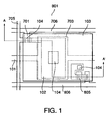
- FIGS. 1 and 2 the first preferred embodiment of an X-ray image detector system according to the present invention will be described below.
- the first preferred embodiment is an X-ray image detector system of a direct conversion system.
- FIG. 1 is a plan view of the X-ray image detector system
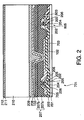
- FIG. 2 is a sectional view taken along line A-A' of FIG. 1.
- the X-ray image detector system comprises a plurality of signal lines 705, a plurality of scanning lines 706 formed so as to intersect the signal lines 705, a plurality of pixels 801, each of which is provided at a corresponding one of the intersections between the signal lines 705 and the scanning lines 706 and which are arranged in the form of an array, a bias line 806, an auxiliary capacity line 101, and an X-ray-to-charge converting part.
- each of the signal lines and each of the scanning lines are electrically insulated.
- Each of the pixels 801 comprises a switching element 701 using a thin film transistor (which will be also hereinafter referred to as a "TFT") having an active layer of, e.g., an amorphous silicon, a protecting TFT 805, a pixel capacity 703, an auxiliary electrode 102 formed so as to face the pixel capacity 703, and a pixel electrode 103.
- TFT thin film transistor
- FIG. 1 only one pixel portion is shown, and upper layers than the pixel electrode 103 (e.g., the X-ray-to-charge converting part) are omitted.
- the switching element 701, the protecting TFT 805, the pixel capacity 703, the signal line 705, the scanning line 706, the bias line 806 and the X-ray-to-charge converting part (X-ray-to-charge converting film 802) are connected as shown in FIG. 9. That is, the gate of the switching element 701 is connected to a corresponding one of the scanning lines 706. In addition, one terminal of the source and drain of the switching element 701 is connected to a corresponding one of the signal lines 705, and the other terminal is connected to one end of the X-ray-to-charge converting part and one end of the pixel capacity 703. The other terminal of the switching element 701 is also connected to the gate of the protecting TFT 805 and one terminal of the source and drain thereof. The other terminal of the protecting TFT 805 is connected to the bias line 806.
- Each of the TFT 701, the protecting TFT 805 and the auxiliary electrode 102 is provided with a contact portion 104. Furthermore, it is not always required to provide the pixel capacity 703.
- a metal layer of a metallic material such as MoTa, Ta, TaN, Al, Al alloy, Cu or MoW, or a laminated metal layer of two layers of metallic materials of Ta and TaN x , is deposited on a glass substrate 201 so as to have a thickness of about 300 nm, and etched to form a pattern of the gate electrodes 202 of the switching element 701 and the protecting TFT 805, the scanning line 706, the pixel capacity 703, the pixel capacity line 101 and the bias line 806.
- a metallic material such as MoTa, Ta, TaN, Al, Al alloy, Cu or MoW, or a laminated metal layer of two layers of metallic materials of Ta and TaN x
- an insulator film 203 is deposited by laminating, e.g., an SiO x film having a thickness of about 300 nm and an SiN x film having a thickness of about 50 nm, an amorphous silicon film 204 containing no impurities and having a thickness of about 100 nm, and an SiN x film having a thickness of about 200 nm serving as a stopper 205 are deposited.
- the stopper 205 is aligned with the gate to be patterned using the reverse exposure.
- n + -type amorphous silicon film 206 having a thickness of about 50 nm is deposited, the amorphous silicon film 204 and the n + -type amorphous silicon film 206 are aligned with the TFT to be etched to form islands of an amorphous silicon (active layer).
- the insulator films 203 of the contact portion 104 of the protecting TFT 805 and the contact portion outside of the pixel region are etched to form contact holes, respectively.
- an Mo film having a thickness of about 50 nm, an Al film having a thickness of about 350 nm, and an Mo film having a thickness of about 50 nm or about 20 nm are sputtered and deposited on the whole surface to be patterned to form the auxiliary electrode 102, the signal line 705 and other wiring.
- a film 207a of SiN x having a thickness of about 200 nm is deposited, and a film 207b of benzocyclobutene (BCB) having a thickness of about 1 ⁇ m to about 5 ⁇ m, preferably about 3 ⁇ m, is deposited on the film 207a to form a protective film 207.
- a pixel electrode 103 is formed by an ITO (indium tin oxide) having a thickness of about 100 nm.
- a p-type Se film 208 for contact is deposited on the pixel electrode 103 so as to have a thickness of about 1 to about 100 ⁇ m, preferably about 10 ⁇ m, and an Se film 209 having a resistivity of about 1 x 10 12 to about 1 x 10 16 ⁇ m is deposited thereon so as to have a thickness of about 1 to 300 ⁇ m, preferably about 10 to 100 ⁇ m.
- an Se film 210 having a resistivity of about one-tenth as large as that of the Se film 209 is deposited thereon so as to have a thickness of about 400 ⁇ m to about 1000 ⁇ m, preferably about 900 ⁇ m, and an n-type Se film 211 is deposited thereon so as to have a thickness of about 1 ⁇ m to about 100 ⁇ m, preferably about 10 ⁇ m.
- an Al film having about 100 nm is formed as a common electrode 212.
- the common electrode 212 is connected to a drive circuit (not shown).
- the resistivity of the Se films 209 and 210 is controlled as follows. In the formation of the Se film having a low resistivity, Te of 0 to 30 % by atom is added to Se. Alternatively, As may be added to Se. Since Se is usually p-type, the resistivity of the Se film can be increased by compensating an acceptor by adding an element serving as a donor, e.g., a halogen, such as Cl or I. However, the resistivity of the Se film can be decreased as n-type by further adding the halogen. Alternatively, the resistivity of the Se film may be decreased as p-type by adding an alkali metal, such as Na or K.
- the n-type Se film 211 is formed so as to have a low resistivity by adding a large amount of a halogen, such as Cl or I, to Se to produce a large number of free electrons.
- the p-type Se film 208 is formed so as to have a low resistivity by adding a large amount of an acceptor, such as Na, K or P, to Se to produce a large number of holes.
- FIG. 10 is a graph showing the simulated results of the relationship between the thickness of the Se film 209 and the absolute value of the current multiplication coefficient, using the electric field as a parameter using data for the ionization rate of electrons and positive holes.
- the variation in current multiplication coefficient is preferably small with respect to the variation in thickness of the Se film 209 and the variation in electric field.
- the Se thickness dependency of the current multiplication coefficient decreases to be stable.
- the thickness dependency decreases when the thickness of the Se film 209 is about 1 to 2 ⁇ m or more. If the electric field is 9.0 x 10 7 V/m, the thickness dependency of the current multiplication coefficient is substantially zero when the thickness of the Se film 209 is 300 ⁇ m or more. As the thickness of the Se film increases, the current multiplication coefficient is saturated to be stable. However, if the thickness of the Se film is too large, it is difficult to prepare a power supply for applying a high voltage.
- an electric field of about 1 x 10 7 V/m or higher is preferably applied to the low resistivity Se film.
- the electric field must be 8 x 10 7 V/m or higher, and the electric field dependency of the current multiplication coefficient decreases to be stable as the electric field increases, so that the electric field is preferably 9.0 x 10 7 V/m or higher.
- the voltage applied to the Se film is preferably 10 kV for the case of Se thickness of about 1000 ⁇ m in order to improve the electric charge collecting efficiencies of all of the Se films which needs an electric field of about 1x 10 7 V/m.
- the thickness of the high resistivity Se film is preferably in the range of from about 10 to about 300 ⁇ m. This value may be varied in accordance with the value of the resistivity ratio of the high resistivity film to the low resistivity film.
- the current multiplication factor can be adjusted by the electric field and thickness.
- FIG. 3 shows the relationship between an average electric field applied to the whole film and a signal current at that time, when the X-ray image detector system in this preferred embodiment and the conventional X-ray image detector system are used.
- the Se film 209 was adjusted so as to have a thickness of 100 ⁇ m and a resistivity of 1 x 10 14 ⁇ cm
- the Se film 210 was adjusted so as to have a thickness of 900 ⁇ m and a resistivity of 1 x 10 13 ⁇ m.
- the resistivity was uniform in the X-ray-to-charge converting film 802. Then, the films were irradiated with an X-ray of 500 mL, and a voltage of 1 kV to 13 kV was applied to the common electrode 212 to measure a signal current.
- FIG. 4 is a diagram for explaining the current multiplication effect in this preferred embodiment.
- Se causes a current multiplication.
- the electric field in the Se film 209 exceeds an electric field causing a signal multiplication, so that carrier is multiplied in the Se film 209 to increase the signal current.
- the conventional X-ray-to-charge converting film having a uniform thickness no current multiplication occurs unless the electric field is about ten times as large as that in this preferred embodiment, so that it is difficult to produce a usable high-voltage power supply.
- the thickness is decreased, it is possible to cause current multiplication even if a high-voltage power supply conventionally. However, if the thickness is decreased, it is not possible to absorb a sufficient quantity of X-rays, so that it is not possible to use the X-ray image detector system in good efficiency.
- the two layers of the X-ray-to-charge converting films 209 and 210 having different characteristics are used for the current multiplication function, so that it is possible to obtain a large signal current, i.e., detect an image, even if X-ray irradiation is weak.
- a large signal current i.e., detect an image
- the Se film 208 is a p-type semiconductor
- the Se film 211 is an n-type semiconductor.
- These semiconductor films have the function of improving the ohmic contact of the metal electrode to the X-ray photoelectric transfer film and introducing majority carrier from the metal electrode when X-ray irradiation serving as noises is not carried out, i.e., holding a low OFF-state current.
- the carrier multiplication effect which is the main point of the present invention, is produced by the intermediate high-resistivity semiconductor films 209 and 210.
- a high-resistivity film other than the semiconductor films 208 and 211 may be provided if necessary.
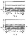
- FIG. 5 is a sectional view in this preferred embodiment.
- the same reference numbers are used for the same portions as those in the first preferred embodiment, and the descriptions thereof are omitted.
- an Se film 501 having a resistivity of about 1 x 10 13 ⁇ m is deposited so as to have a thickness of about 100 ⁇ m.
- an Se film 502 having a resistivity of about 1 x 10 14 ⁇ m is deposited so as to have a thickness of about 10 ⁇ m
- an Se film 503 having a resistivity of about 1 x 10 13 ⁇ m is deposited so as to have a thickness of about 900 ⁇ m.
- an n-type Se film 211 and a common electrode 212 are formed.
- a current multiplication type sensitizing film has a high electric field, and the electric field concentrates on the non-uniform portion of the film of the contact portion 104 or the like, so that there is some possibility of causing dielectric breakdown.
- the current multiplication region is separated from the contact portion 104 to be provided between the films, so that the irregularity decreases to inhibit the concentration of the electric field.
- the current multiplication is mainly carried out by a hole 401. Therefore, the greater multiplication factor of the Se film 502 increases as the distance between the Se film 502 and the pixel electrode 103 decreases, since more holes 401 are produced by the absorbed X-rays.
- the Se film 502 is preferably arranged nearer to the pixel electrode 103 than the center of the thickness of the Se film.
- the multiplication factor is sufficiently large, it is possible to select an appropriate position by adjusting the voltage characteristics and the multiplication factor.
- the construction of the pixel is the same as that in the first preferred embodiment as shown in FIGS. 1 and 9.
- the cross section of this preferred embodiment is shown in FIG. 6.
- the same reference numbers are used for the same portions as those in the second preferred embodiment, and the descriptions thereof are omitted.
- This preferred embodiment is the same as the second preferred embodiment, except that the recess in the contact portion 104 of the pixel electrode 103 is electroplated with Sn, Ni, Cu or the like to be flattened and a liquid conductive material is embedded. This is carried out to flatten the contact portion 104 to prevent the concentration of the electric field, similar to the second preferred embodiment. Also in this preferred embodiment, it is possible to multiply signals and it is possible to withstand a high voltage similar to the second preferred embodiment.
- the material of the X-ray-to-charge converting film should not be limited to Se as long as the film has the multiplication effect.
- the material of the X-ray-to-charge converting film may be selected from the group consisting of As-Te-Se alloy, Se containing an impurity, such as a halogen, As-Te-Se alloy, HgI 2 and Te.
- the thickness of the X-ray-to-charge converting film may be selected so as to sufficiently absorb used X-rays.
- the X-ray-to-charge converting film may comprise two or more layers having suitably selected resistivity and thickness.
- the electric field strength for avalanche multiplication has been 9 x 10 7 V/cm or higher when the material of the film is Se
- the electric field may be suitably adjusted in accordance with the kind of the X-ray-to-charge converting transfer film and the added impurity.
- the conductive type of the X-ray-to-charge converting film should not be limited to n-i-p-type in this preferred embodiment, it may be p-i-n-type or another type.
- the i-type means an intrinsic semiconductor.
- the i layer, to which a high electric field is applied has only to comprise two or more layers of high resistivity and low resistivity layers.
- the current multiplication effect as described in detail is effective in any array structures since it does not depend on the array structure of the underlayer. While the direct conversion type has been described, the above-described current multiplication effect is also applicable in the indirect conversion type.
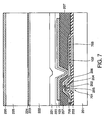
- the photoelectric transfer part may comprise a first photoelectric transfer film having an adjusted thickness and resistivity, and a second photoelectric transfer film having an adjusted thickness and resistivity. In this case, a high electric field exists in the first photoelectric transfer film, so that the signal current increases. Referring to FIG. 7, such a construction will be described as an example of a photoelectric transfer film of an amorphous silicon.
- FIG. 7 is a sectional view of the fourth preferred embodiment of an X-ray image detector system of an indirect conversion type according to the present invention.
- a metal layer of a metallic material such as MoTa, Ta, TaN, Al, Al alloy, Cu or Mow, or a laminated metal layer of two layers of metallic materials of Ta and TaNx, is deposited on a glass substrate 201 so as to have a thickness of about 300 nm, and etched to form a pattern of the gate electrode 202 of a switching element 701, a scanning line 706, a pixel capacity 703 and a pixel capacity line (not shown).
- an insulator film 203 is deposited by laminating an SiO x film having a thickness of about 300 nm and an SiN x film having a thickness of about 50 nm, an amorphous silicon film 204 containing no impurities and having a thickness of about 100 nm, and an SiN x film having a thickness of about 200 nm serving as a stopper 205 are deposited.
- the stopper 205 is aligned with the gate to be patterned using the reverse exposure.
- n + -type amorphous silicon film 206 having a thickness of about 50 nm is deposited, the amorphous silicon film 204 and the n + -type amorphous silicon film 206 are aligned with the TFT to be etched to form islands of an amorphous silicon (active layer).
- the insulator film 203 of the contact portion outside of the pixel area are etched to form contact holes.
- an Mo film having a thickness of about 50 nm, an Al film having a thickness of about 350 nm, and an Mo film having a thickness of about 50 nm or about 20 nm are sputtered and deposited on the whole surface to be patterned to form an auxiliary electrode 102, a signal line 705 and other wiring.
- an ITO having a thickness of about 100 nm is deposited to be patterned to form a pixel electrode 103. Since a high voltage is not applied to a photoelectric transfer film of an indirect conversion type, a protecting diode for preventing the pixel potential from being a high potential is not provided.
- a p-type amorphous silicon film 220 for contact is deposited on the pixel electrode 103 so as to have a thickness of about 10 nm to about 300 nm, preferably about 200 nm, and an amorphous silicon film 221 having a resistivity of about 1 x 10 10 to about 1 x 10 13 ⁇ m is deposited thereon so as to have a thickness of about 100 nm to about 500 nm, preferably about 200 nm.
- an amorphous silicon film 222 having a resistivity of about one-tenth as large as that of the amorphous silicon film 221 is deposited on the amorphous silicon film 221 so as to have a thickness of about 900 nm to about 4500 nm, preferably about 2 ⁇ m.
- a common electrode 224 of ITO having a thickness of about 100 nm is formed on the common electrode 224.
- a phosphor 225 for X-rays of CsI or Gd 2 O 2 S (gadolinium oxysulfide) is deposited so as to have a thickness of about 100 ⁇ m to 1000 ⁇ m.
- a reflective layer 230 of Al for reflection of fluorescence is deposited thereon so as to have a thickness of about 100 nm.
- the common electrode 224 and so forth are connected to a drive circuit (not shown).
- the resistivity of the amorphous silicon films is controlled as follows. In the formation of the low resistivity layer, P or B of about 1000 ppm to about 5 % by atom is added to the amorphous silicon for n-type or p-type, respectively. Since an amorphous silicon containing no impurities usually has a weak n-type, the resistivity of the amorphous silicon film can be increased by adding B of about 10 to 500 ppm of an acceptor. Because the resistivity of the amorphous silicon film can be increased by adding B of the acceptor since the amorphous silicon film usually has an n-type.
- the material of the photoelectric transfer film should not be limited to amorphous silicon as long as the film has the multiplication effect.
- the material of the photoelectric transfer film may be selected from the group consisting of CdSe, CdTe, an alloy of amorphous silicon, C and Ge, GaAs, and amorphous GaN.
- the impurity may be suitably added in the above material.
- the thickness of the photoelectric transfer film may be selected so as to sufficiently absorb luminescent light.
- the photoelectric transfer film may comprise two or more layers having suitably selected resistivity and thickness so as to form an electric field wherein current is multiplied. The multiplied electric field may be suitably adjusted in accordance with the kind of the photoelectric transfer film and the added impurity.
- the conductive type of the photoelectric transfer film should not be limited to n-i-p-type in this preferred embodiment, it may be p-i-n-type or another type.
- the i layer, to which a high electric field is applied, should be composed of two or more layers of high resistivity and low resistivity layers.
- the TFT may be formed of a polysilicon. If the TFT is formed of a polysilicon, the size of the TFT can be decreased, so that the effective area of each pixel can be increased. In addition, since peripheral circuits can be prepared on the same glass substrate, it is possible to decrease the production costs including the costs for the peripheral circuits. Furthermore, the structure of the TFT may be either an upper gate type or a lower gate type.
- the X-ray-to-charge converting film may be formed of amorphous Se, an alloy of Se and Te or As, amorphous Si, amorphous Te, PbI 2 , or HgI 2 .
- the X-ray-to-charge converting film or the photoelectric transfer film has current multiplication characteristics to increase the signal intensity to be resistant to noises. Therefore, it is possible to detect weak signals, so that it is possible to detect an image even in the case of weak X-irradiation. Thus, it is possible to use the X-ray image detect system in a more safe state to human bodies.
Description
- The present invention relates generally to an X-ray image detector system. More specifically, the invention relates to an X-ray image detector system for use in an X-ray diagnosing system for medical use.
- In recent years, in the field of medical treatment, the database of medical data for patients makes progress in order to rapidly and precisely carry out medical treatment. Patients usually receive diagnostics of a plurality of medical treatment facilities. In such a case, if there are no data of other medical treatment facilities, there is some possibility that medical treatment can not be precisely carried out. As an example, there is a problem of medicines or drugs. It is required to take account of drugs administered in other medical treatment facilities to administer appropriate drugs to carry out medical treatment.
- It is also required to make database for image data of radiography. In accordance with this database system, it is desired to digitize X-ray images. In an X-ray diagnosing system for medical use, a silver halide film is conventionally used to detect an image. In order to digitize this diagnostic data, it is required to scan the film by a scanner after developing the film, so that it takes a great deal of time. Recently, there is realized a system for directly digitizing an image using a CCD camera having a size of about one inch and an image intensifier tube. However, when an image of, such as a lung, is detected by this system, it is required to provide an optical system for condensing light to detect an image of a region of about 40 cm x 40 cm, so that there is a problem of increasing the system size. There is also a problem in that resolution decreases due to the distortion of an optical system.
- In order to solve these problems, there is proposed a flat-panel X-ray detector of an indirect conversion system using a thin film transistor (which will be hereinafter referred to as a "TFT") having an active layer of an amorphous silicon as a switching element (see, e.g., U.S. Patent No. 4,689,487).
- FIG. 8 shows a circuit construction of this flat-panel X-ray detector, and the operation thereof will be described below.
- This flat-panel X-ray detector is a detector of an indirect conversion system for converting an incident X-ray into luminescent light by means of a phosphor or the like to change the converted light to an electric charge by means of a photoelectric transfer film of each pixel (picture element). This flat-panel X-ray detector has pixels el,l, ···, em,n arranged in the form of an array wherein hundreds to thousands pixels are arranged on each side. Each element ei,j (i = 1, ···, m, j = 1, ···, n) has a
TFT 701, aphotoelectric transfer film 702 and apixel capacity 703. Thephotoelectric transfer film 702 and thepixel capacity 703 are connected in parallel. To one end thereof, a negative bias voltage is applied by means of apower supply 704, and the other end is connected to one of the source and drain of theTFT 701. The other end of the source and drain of the TFT 701 is connected to asignal line 705, and the gate of the TFT 701 is connected to ascanning line 706. The on/off of the TFT 701 is controlled by a scanningline driving circuit 707. The terminal of thesignal line 705 is connected to anamplifier 710 for signal detection via aswitch 709 controlled by a signalline control circuit 708. - If X-rays are incident on the flat-panel X-ray detector, the phosphor irradiated with the X-rays emits light, and the emitted light is converted into an electric charge by means of the
photoelectric transfer film 702, so that the electric charge accumulates in thepixel capacity 703. When onescanning line 706 is driven by the scanningline driving circuit 701 so that all ofTFTs 701 connected to thescanning line 706 are turned on, the accumulating charge is transferred to theamplifier 710 via thesignal line 705. Then, the electric charge for each pixel is inputted to theamplifier 710 by means of theswitch 709 to be converted to dot sequential signals capable of being displayed on a CRT or the like. The quantity of electric charge varies in accordance with the quantity of light being incident on each pixel ei,j (i = 1, ···, m, j = 1, ···, n), so that the amplitude of output of theamplifier 710 varies. - The flat-panel X-ray detector of the indirect conversion system shown in FIG. 8 can directly form a digital image by the A/D conversion of the output signal of the
amplifier 710. Moreover, it is possible to produce a pixel region of a thin and large-screen by the array of theTFTs 701. - There are other flat-panel X-ray detectors of a direct conversion system for directly converting X-rays being incident on pixels into an electric charge.
- The flat-panel X-ray detector of this direct conversion system has no phosphor. At this point, the flat-panel X-ray detector of the direct conversion system is different from that of the above-described indirect conversion system. In addition, in the flat-panel X-ray detector of the direct conversion system, the magnitude of a bias applied to a photoelectric transfer film or an X-ray-to-charge converting film is different from that in the indirect conversion system.
- In the case of the indirect conversion system, a bias of several volts to over ten volts is applied to the photoelectric transfer film. When fluorescence enters the photoelectric transfer film, the electric charge accumulates in the pixel capacity provided in parallel to the photoelectric transfer film in each pixel. In this case, the voltage applied to the pixel capacity is a bias of several volts to over ten volts applied to the photoelectric transfer film at the maximum.
- On the other hand, in the direct conversion system; the X-ray-to-charge converting film, the pixel capacity and the TFT serving as a switch for each pixel are connected in series, and a high bias of several kV is applied thereto. Therefore, when X-rays are incident on the pixel, the electric charge produced by the X-ray-to-charge converting film accumulates in the pixel capacity. However, if the quantity of incident X-ray is excessive, the electric charge accumulating in the pixel capacity increases, so that it is afraid that a high voltage of more than 10 kV is applied to the insulator films of the pixel capacity and the TFT to cause electrical break-down. For that reason, the direct conversion system must take measures to prevent an excessive voltage from being applied to the pixel capacity and TFTs.
- Therefore, a protecting TFT serving as a protecting non-linear element is provided in each of pixels. Thus, when excessive X-rays enter a pixel, a higher electric charge than that defined by a bias is discharged to the outside of the pixel via the protecting TFT to prevent the dielectric breakdown of the TFT and pixel capacity.
- FIG. 9 shows the construction of a pixel of a flat-panel X-ray detector of a direct conversion system using the protecting TFT, and the operation thereof will be described below.
- Each
pixel 801 of a flat-panel X-ray detector of a direct conversion system shown in FIG. 9 comprises aTFT 701 used as a switching element, an X-ray-to-charge converting film 802, and apixel capacity 703. Similar to the X-ray detector shown in FIG. 8, thepixels 801 are arranged in the form of an array. Thepixel capacity 703 is connected to apixel capacity bias 803. To the X-ray-to-charge converting film 802, a negative bias voltage is applied by a high-voltage power supply 804. The gate of the TFT 701 is connected to ascanning line 706, and one of the source and drain of theTFT 701 is connected to asignal line 705, so that the on/off of theTFT 701 is controlled by means of a scanningline driving circuit 707. The terminal of thesignal line 705 is connected to anamplifier 710 for signal detection. A protecting TFT 805 is biased by apower supply 807 via abias line 806. The protecting TFT 805 allows an electric charge of a bias voltage or higher to escape through thebias line 806. - In both of the X-ray image detector systems using the flat-panel X-ray detectors of the direct and indirect conversion systems using the
TFTs 701, very weak signals can not be detected, so that there is a lower limit to the X-ray irradiation intensity to a human body. Because a signal voltage shift is produced by a floating capacity which is received by thesignal line 705 from the intersectingscanning line 706 and thebias line 806, and because there is a limit to the reduction of noises of theamplifier 710 for signal detection and noises due to leak currents or the like of the protectingTFT 805 used for the flat-panel X-ray detector of the direct conversion system. In order to solve this problem, it is considered that an amplifier circuit for amplifying the electric charge produced in thephotoelectric transfer film 702 or X-ray-to-charge converting film 802 is provided for eachpixel 801. However, it is difficult to realize this since the amplifier circuit is prepared by the same design rule as that of the TFTs for pixels to cause the area of only the amplifier circuit to be greater than the pixel area. - US 5,198,673 discloses a radiation image detector with optical gain selenium photosensors and a scintillator. High voltage is applied at the selenium photosensor to cause the photosensor to exhibit avalanche multiplication. The photosensor material is advantageously doped with arsenic and a relatively small portion adjoining a barrier layer is doped with lithium fluoride.
- Further, US 5,164,809 discloses amorphous silicon radiation detectors with transversely oriented electrode layers. The structure of the detector allows high electric fields resulting in a reduction in noise and increase in signal including avalanche multiplication. One embodiment of a detector shows a PIPN structure with layers of varying conductivity sandwiched between electrodes.
- Additionally, US 5,396,072 discloses an X-ray image detector comprising a plurality of X-ray-sensitive sensors each one having an electrode and a switching element connected to an output lead. A photo-conductor layer is provided between the collecting electrodes and a bias electrode. The photo-conductor layer consists of amorphous selenium with an addition of arsenic. On top of this layer, there is provided another semiconductor layer doped with alkali metal not conducting positive charge carriers.
- It is therefore an object of the present invention to eliminate the aforementioned problems and to provide an X-ray detector system capable of picking up an image even if X-ray irradiation is weak.
- This object is achieved by an X-ray image detector system having the features of
independent claim 1. - One embodiment of an X-ray image detector system comprises: a plurality of scanning lines; a plurality of signal lines formed so as to intersect the scanning lines; and a plurality of pixel parts, each of which is toned at a corresponding one of the intersections between the scanning lines and the signal lines so as to form an array; each of said pixel parts having an X-ray-to-charge converting part for converting an incident X-ray to an electric charge, a pixel electrode for receiving the electric charge from the X-ray-to-charge converting part, and a switching element which is operated on the basis of a signal of a corresponding one of the scanning lines, one end of the switching element being connected to the pixel electrode, and the other end of the switching element is connected to a corresponding one of the signal lines, wherein the X-ray-to-charge converting part includes at least a first X-ray-to-charge converting film, and a second X-ray-to-charge converting film having a lower resistivity than that of the first X-ray-to-charge converting film.
- Furthermore, an electric field for causing a current multiplication is preferably applied to the first X-ray-to-charge converting film.
- In addition, each of the first and second X-ray-to-charge converting films is preferably formed of Se, and the electric field for causing the current multiplication is preferably 9 x 10⁷ V/m.
- The X-ray-to-charge converting part may have a third X-ray-to-charge converting film of a first conductive type formed between the pixel electrode and the first X-ray-to-charge converting film, and a fourth X-ray-to-charge converting film of a second conductive type formed on the second X-ray-to-charge converting film, the second X-ray-to-charge converting film being formed on the first X-ray-to-charge converting film.
- The X-ray-to-charge converting part may have a fifth X-ray-to-charge converting film having a lower resistivity than that of the first X-ray-to-charge converting film between the third X-ray-to-charge converting film and the first X-ray-to-charge converting film. For example, if the X-ray-to-charge converting film is formed of Se, each of the first, second and fifth X-ray-to-charge converting films often have a high resistivity, and is often formed of an i-type (intrinsic) semiconductor containing no intentionally doped impurities decreasing resistivity, or an i-type semiconductor containing a small amount of impurity. On the other hand, the third and fourth X-ray-to-charge converting films are often formed of an n-type semiconductor containing a large amount of donor impurity, or a p-type semiconductor containing a large amount of acceptor impurity. The third and fourth X-ray-to-charge converting films can decrease the resistivity to the upper or lower metal electrode to form an ohmic contact and can decrease the dark current during no X-ray irradiation serving as a noise source. Therefore, the third and fourth X-ray-to-charge converting films have the function of preventing majority carrier from being introduced from the electrode. The third and fourth X-ray-to-charge converting films may be formed of any materials of these effects.
- Furthermore, at least one boundary surface of the first X-ray-to-charge converting film is preferably flattened.
- In addition, the first X-ray-to-charge converting film preferably have a non-flat portion on the boundary surface, the non-flat portion being filled with a conductive material.
- Moreover, the thickness of the fifth X-ray-to-charge converting film is preferably smaller than the thickness of the second X-ray-to-charge converting film.
- According to another embodiment, an X-ray image detector system comprises: a plurality of scanning lines; a plurality of signal lines formed so as to intersect the scanning lines; a plurality of pixel parts, each of which is formed at a corresponding one of the intersections between the scanning lines and the signal lines so as to form an array; each of said pixel parts having an X-ray-to-luminescent light converting part for converting an incident X-ray to luminescent light, a photoelectric transfer part, formed on the plurality of pixel parts, for converting the luminescent light, which is converted by the X-ray-to-luminescent light converting part, to an electric charge, a pixel electrode for receiving the electric charge from the photoelectric transfer part, and a switching element which is operated on the basis of a signal of a corresponding one of the scanning lines, one end of the switching element being connected to the pixel electrode, and the other end of the switching element being connected to a corresponding one of the signal lines, wherein the photoelectric transfer part includes at least a first photoelectric transfer film, and a second photoelectric transfer film having a lower resistivity than that of the first photoelectric transfer film.
- The present invention will be understood more fully from the detailed description given herebelow and from the accompanying drawings of the preferred embodiments of the invention. However, the drawings are not intended to imply limitation of the invention to a specific embodiment, but are for explanation and understanding only.
- In the drawings:
- FIG. 1 is a plan view of the first preferred embodiment of an X-ray image detector system according to the present invention;
- FIG. 2 is a sectional view of the first preferred embodiment of an X-ray image detector system according to the present invention, which is taken along line A-A' of FIG. 1.
- FIG. 3 is a characteristic diagram of an X-ray-to-charge converting film for use in the present invention;
- FIG. 4 is a band diagram for explaining an current multiplication effect;
- FIG. 5 is a sectional view of the second preferred embodiment of an X-ray image detector system according to the present invention;
- FIG. 6 is a sectional view of the third preferred embodiment of an X-ray image detector system according to the present invention;
- FIG. 7 is a sectional view of the fourth preferred embodiment of an X-ray image detector system according to the present invention;
- FIG. 8 is a circuit diagram of an X-ray image detector system of an indirect conversion type;
- FIG. 9 is a circuit diagram of an X-ray image detector system of a direct conversion type; and
- FIG. 10 is a graph showing the simulated results of the relationship between the thickness of an Se film and the absolute value of a current multiplication coefficient, using an electric field as a parameter.
- Referring now to the accompanying drawings, the preferred embodiments of an X-ray image detector system according to the present invention will be described in detail below. The present invention should not be limited to these preferred embodiments.
- Referring to FIGS. 1 and 2, the first preferred embodiment of an X-ray image detector system according to the present invention will be described below.
- The first preferred embodiment is an X-ray image detector system of a direct conversion system. FIG. 1 is a plan view of the X-ray image detector system, and FIG. 2 is a sectional view taken along line A-A' of FIG. 1. In the first preferred embodiment, the X-ray image detector system comprises a plurality of
signal lines 705, a plurality ofscanning lines 706 formed so as to intersect thesignal lines 705, a plurality ofpixels 801, each of which is provided at a corresponding one of the intersections between thesignal lines 705 and thescanning lines 706 and which are arranged in the form of an array, abias line 806, anauxiliary capacity line 101, and an X-ray-to-charge converting part. Furthermore, each of the signal lines and each of the scanning lines are electrically insulated. - Each of the
pixels 801 comprises aswitching element 701 using a thin film transistor (which will be also hereinafter referred to as a "TFT") having an active layer of, e.g., an amorphous silicon, a protectingTFT 805, apixel capacity 703, anauxiliary electrode 102 formed so as to face thepixel capacity 703, and apixel electrode 103. However, in FIG. 1, only one pixel portion is shown, and upper layers than the pixel electrode 103 (e.g., the X-ray-to-charge converting part) are omitted. - The switching
element 701, the protectingTFT 805, thepixel capacity 703, thesignal line 705, thescanning line 706, thebias line 806 and the X-ray-to-charge converting part (X-ray-to-charge converting film 802) are connected as shown in FIG. 9. That is, the gate of theswitching element 701 is connected to a corresponding one of the scanning lines 706. In addition, one terminal of the source and drain of theswitching element 701 is connected to a corresponding one of thesignal lines 705, and the other terminal is connected to one end of the X-ray-to-charge converting part and one end of thepixel capacity 703. The other terminal of theswitching element 701 is also connected to the gate of the protectingTFT 805 and one terminal of the source and drain thereof. The other terminal of the protectingTFT 805 is connected to thebias line 806. - Each of the
TFT 701, the protectingTFT 805 and theauxiliary electrode 102 is provided with acontact portion 104. Furthermore, it is not always required to provide thepixel capacity 703. - Referring to the sectional view of FIG. 2, the detailed construction will be described below.
- A metal layer of a metallic material, such as MoTa, Ta, TaN, Al, Al alloy, Cu or MoW, or a laminated metal layer of two layers of metallic materials of Ta and TaNx, is deposited on a
glass substrate 201 so as to have a thickness of about 300 nm, and etched to form a pattern of thegate electrodes 202 of theswitching element 701 and the protectingTFT 805, thescanning line 706, thepixel capacity 703, thepixel capacity line 101 and thebias line 806. Then, using the plasma chemical vapor deposition (plasma CVD), after aninsulator film 203 is deposited by laminating, e.g., an SiOx film having a thickness of about 300 nm and an SiNx film having a thickness of about 50 nm, anamorphous silicon film 204 containing no impurities and having a thickness of about 100 nm, and an SiNx film having a thickness of about 200 nm serving as astopper 205 are deposited. Thestopper 205 is aligned with the gate to be patterned using the reverse exposure. - Then, after an n+-type
amorphous silicon film 206 having a thickness of about 50 nm is deposited, theamorphous silicon film 204 and the n+-typeamorphous silicon film 206 are aligned with the TFT to be etched to form islands of an amorphous silicon (active layer). Theinsulator films 203 of thecontact portion 104 of the protectingTFT 805 and the contact portion outside of the pixel region are etched to form contact holes, respectively. Subsequently, an Mo film having a thickness of about 50 nm, an Al film having a thickness of about 350 nm, and an Mo film having a thickness of about 50 nm or about 20 nm are sputtered and deposited on the whole surface to be patterned to form theauxiliary electrode 102, thesignal line 705 and other wiring. - Then, a
film 207a of SiNx having a thickness of about 200 nm is deposited, and afilm 207b of benzocyclobutene (BCB) having a thickness of about 1 µm to about 5 µm, preferably about 3 µ m, is deposited on thefilm 207a to form aprotective film 207. After contact holes are formed in theTFT 701, the protectingTFT 805 and theauxiliary electrode 102, apixel electrode 103 is formed by an ITO (indium tin oxide) having a thickness of about 100 nm. - A p-
type Se film 208 for contact is deposited on thepixel electrode 103 so as to have a thickness of about 1 to about 100 µm, preferably about 10 µm, and anSe film 209 having a resistivity of about 1 x 10¹² to about 1 x 10¹⁶ Ωm is deposited thereon so as to have a thickness of about 1 to 300 µm, preferably about 10 to 100 µm. Then, anSe film 210 having a resistivity of about one-tenth as large as that of theSe film 209 is deposited thereon so as to have a thickness of about 400 µm to about 1000 µm, preferably about 900 µm, and an n-type Se film 211 is deposited thereon so as to have a thickness of about 1 µm to about 100 µm, preferably about 10 µm. Thereafter, an Al film having about 100 nm is formed as acommon electrode 212. Finally, thecommon electrode 212 is connected to a drive circuit (not shown). - The resistivity of the
Se films type Se film 211 is formed so as to have a low resistivity by adding a large amount of a halogen, such as Cl or I, to Se to produce a large number of free electrons. In addition, the p-type Se film 208 is formed so as to have a low resistivity by adding a large amount of an acceptor, such as Na, K or P, to Se to produce a large number of holes. - Referring to FIG. 10, the preferred thickness of the
Se film 209 having a high resistivity will be described. FIG. 10 is a graph showing the simulated results of the relationship between the thickness of theSe film 209 and the absolute value of the current multiplication coefficient, using the electric field as a parameter using data for the ionization rate of electrons and positive holes. In order to obtain a stable operation of the detector and a good image, the variation in current multiplication coefficient is preferably small with respect to the variation in thickness of theSe film 209 and the variation in electric field. As can be seen from FIG. 10, as the thickness of theSe film 209 increases, the Se thickness dependency of the current multiplication coefficient decreases to be stable. If the electric field is 1.5 x 10⁸ V/m, the thickness dependency decreases when the thickness of theSe film 209 is about 1 to 2 µm or more. If the electric field is 9.0 x 10⁷ V/m, the thickness dependency of the current multiplication coefficient is substantially zero when the thickness of theSe film 209 is 300 µm or more. As the thickness of the Se film increases, the current multiplication coefficient is saturated to be stable. However, if the thickness of the Se film is too large, it is difficult to prepare a power supply for applying a high voltage. - In order to improve the electric charge collecting efficiency, an electric field of about 1 x 10⁷ V/m or higher is preferably applied to the low resistivity Se film. The electric field must be 8 x 10⁷ V/m or higher, and the electric field dependency of the current multiplication coefficient decreases to be stable as the electric field increases, so that the electric field is preferably 9.0 x 10⁷ V/m or higher. The voltage applied to the Se film is preferably 10 kV for the case of Se thickness of about 1000 µm in order to improve the electric charge collecting efficiencies of all of the Se films which needs an electric field of about 1x 10⁷ V/m. For that reason, taking account of the safety with respect to the variation in thickness and electric field, if the resistivity ratio of the high resistivity Se film to the low resistivity Se film is in the range of from about 10 to about 100, the thickness of the high resistivity Se film is preferably in the range of from about 10 to about 300 µm. This value may be varied in accordance with the value of the resistivity ratio of the high resistivity film to the low resistivity film. The current multiplication factor can be adjusted by the electric field and thickness.
- FIG. 3 shows the relationship between an average electric field applied to the whole film and a signal current at that time, when the X-ray image detector system in this preferred embodiment and the conventional X-ray image detector system are used. In the X-ray image detector system in this preferred embodiment, the
Se film 209 was adjusted so as to have a thickness of 100 µm and a resistivity of 1 x 10¹⁴ Ωcm, and theSe film 210 was adjusted so as to have a thickness of 900 µm and a resistivity of 1 x 10¹³ Ωm. In the conventional X-ray image detector system, the resistivity was uniform in the X-ray-to-charge converting film 802. Then, the films were irradiated with an X-ray of 500 mL, and a voltage of 1 kV to 13 kV was applied to thecommon electrode 212 to measure a signal current. - As a result, when the average electric field was about 1 x 10⁷ V/m, there was a difference between the signal current 301 and the signal current 302 when the X-ray image detector system in this preferred embodiment and the conventional X-ray image detector system were used, respectively. When an average electric field of about 1 x 10⁷ V/m was applied in the X-ray image detector system this preferred embodiment, an electric field of about 1 x 10⁸ V/m is applied to the
Se film 209, and an electric field of about 1 x 10⁷ V/m is applied to theSe film 210. - FIG. 4 is a diagram for explaining the current multiplication effect in this preferred embodiment. When an average electric field of about 9 x 10⁷ V/m or higher is applied, Se causes a current multiplication. In this preferred embodiment, as shown in FIG. 4, the electric field in the
Se film 209 exceeds an electric field causing a signal multiplication, so that carrier is multiplied in theSe film 209 to increase the signal current. On the other hand, in the conventional X-ray-to-charge converting film having a uniform thickness, no current multiplication occurs unless the electric field is about ten times as large as that in this preferred embodiment, so that it is difficult to produce a usable high-voltage power supply. In addition, if the thickness is decreased, it is possible to cause current multiplication even if a high-voltage power supply conventionally. However, if the thickness is decreased, it is not possible to absorb a sufficient quantity of X-rays, so that it is not possible to use the X-ray image detector system in good efficiency. - Therefore, in this preferred embodiment, the two layers of the X-ray-to-
charge converting films - Furthermore, in the above-described preferred embodiment, the
Se film 208 is a p-type semiconductor, and theSe film 211 is an n-type semiconductor. These semiconductor films have the function of improving the ohmic contact of the metal electrode to the X-ray photoelectric transfer film and introducing majority carrier from the metal electrode when X-ray irradiation serving as noises is not carried out, i.e., holding a low OFF-state current. The carrier multiplication effect, which is the main point of the present invention, is produced by the intermediate high-resistivity semiconductor films semiconductor films - Referring to FIG. 5, the second preferred embodiment of an X-ray image detector system according to the present invention will be described below. The construction of the pixel is the same as that in the first preferred embodiment, and shown in FIGS. 1 and 9. FIG. 5 is a sectional view in this preferred embodiment. The same reference numbers are used for the same portions as those in the first preferred embodiment, and the descriptions thereof are omitted.
- In this preferred embodiment, after a p-
type Se film 208 for contact is deposited similar to the first preferred embodiment, anSe film 501 having a resistivity of about 1 x 10¹³ Ωm is deposited so as to have a thickness of about 100 µm. Then, after anSe film 502 having a resistivity of about 1 x 10¹⁴ Ωm is deposited so as to have a thickness of about 10 µm, anSe film 503 having a resistivity of about 1 x 10¹³ Ωm is deposited so as to have a thickness of about 900 µm. Moreover, similar to the first preferred embodiment, an n-type Se film 211 and acommon electrode 212 are formed. In general, a current multiplication type sensitizing film has a high electric field, and the electric field concentrates on the non-uniform portion of the film of thecontact portion 104 or the like, so that there is some possibility of causing dielectric breakdown. In this preferred embodiment, in order to avoid this breakdown, the current multiplication region is separated from thecontact portion 104 to be provided between the films, so that the irregularity decreases to inhibit the concentration of the electric field. - The current multiplication is mainly carried out by a
hole 401. Therefore, the greater multiplication factor of theSe film 502 increases as the distance between theSe film 502 and thepixel electrode 103 decreases, sincemore holes 401 are produced by the absorbed X-rays. Thus, theSe film 502 is preferably arranged nearer to thepixel electrode 103 than the center of the thickness of the Se film. However, since the multiplication factor is sufficiently large, it is possible to select an appropriate position by adjusting the voltage characteristics and the multiplication factor. - Also in this preferred embodiment, it is possible to obtain the same multiplication effect as that in the first preferred embodiment, and it is possible to more stably withstand a high voltage, so that it is possible to realize a more stable operation.
- Referring to FIG. 6, the third preferred embodiment of an X-ray detector system according to the present invention will be described below.
- The construction of the pixel is the same as that in the first preferred embodiment as shown in FIGS. 1 and 9. The cross section of this preferred embodiment is shown in FIG. 6. The same reference numbers are used for the same portions as those in the second preferred embodiment, and the descriptions thereof are omitted.
- This preferred embodiment is the same as the second preferred embodiment, except that the recess in the
contact portion 104 of thepixel electrode 103 is electroplated with Sn, Ni, Cu or the like to be flattened and a liquid conductive material is embedded. This is carried out to flatten thecontact portion 104 to prevent the concentration of the electric field, similar to the second preferred embodiment. Also in this preferred embodiment, it is possible to multiply signals and it is possible to withstand a high voltage similar to the second preferred embodiment. - Furthermore, the material of the X-ray-to-charge converting film should not be limited to Se as long as the film has the multiplication effect. For example, the material of the X-ray-to-charge converting film may be selected from the group consisting of As-Te-Se alloy, Se containing an impurity, such as a halogen, As-Te-Se alloy, HgI2 and Te. The thickness of the X-ray-to-charge converting film may be selected so as to sufficiently absorb used X-rays. The X-ray-to-charge converting film may comprise two or more layers having suitably selected resistivity and thickness. While the electric field strength for avalanche multiplication has been 9 x 10⁷ V/cm or higher when the material of the film is Se, the electric field may be suitably adjusted in accordance with the kind of the X-ray-to-charge converting transfer film and the added impurity. In addition, the conductive type of the X-ray-to-charge converting film should not be limited to n-i-p-type in this preferred embodiment, it may be p-i-n-type or another type. The i-type means an intrinsic semiconductor. The i layer, to which a high electric field is applied, has only to comprise two or more layers of high resistivity and low resistivity layers.
- The current multiplication effect as described in detail is effective in any array structures since it does not depend on the array structure of the underlayer. While the direct conversion type has been described, the above-described current multiplication effect is also applicable in the indirect conversion type.
- In an X-ray image detector system of an indirect conversion type, when X-rays are incident thereon, a phosphor irradiated with X-rays emits fluorescence, which is converted into an electric charge by means of a photoelectric transfer part. This electric charge produces a signal current to be taken out similar to the X-ray image detector system of the direct conversion type. Thus, in order to carry out signal multiplication in the X-ray image detector system of the indirect conversion type according to the present invention, the photoelectric transfer part may comprise a first photoelectric transfer film having an adjusted thickness and resistivity, and a second photoelectric transfer film having an adjusted thickness and resistivity. In this case, a high electric field exists in the first photoelectric transfer film, so that the signal current increases. Referring to FIG. 7, such a construction will be described as an example of a photoelectric transfer film of an amorphous silicon.
- FIG. 7 is a sectional view of the fourth preferred embodiment of an X-ray image detector system of an indirect conversion type according to the present invention. As shown in FIG. 7, a metal layer of a metallic material, such as MoTa, Ta, TaN, Al, Al alloy, Cu or Mow, or a laminated metal layer of two layers of metallic materials of Ta and TaNx, is deposited on a
glass substrate 201 so as to have a thickness of about 300 nm, and etched to form a pattern of thegate electrode 202 of aswitching element 701, ascanning line 706, apixel capacity 703 and a pixel capacity line (not shown). Then, using the plasma CVD method, after aninsulator film 203 is deposited by laminating an SiOx film having a thickness of about 300 nm and an SiNx film having a thickness of about 50 nm, anamorphous silicon film 204 containing no impurities and having a thickness of about 100 nm, and an SiNx film having a thickness of about 200 nm serving as astopper 205 are deposited. Thestopper 205 is aligned with the gate to be patterned using the reverse exposure. Then, after an n+-typeamorphous silicon film 206 having a thickness of about 50 nm is deposited, theamorphous silicon film 204 and the n+-typeamorphous silicon film 206 are aligned with the TFT to be etched to form islands of an amorphous silicon (active layer). Theinsulator film 203 of the contact portion outside of the pixel area are etched to form contact holes. Subsequently, an Mo film having a thickness of about 50 nm, an Al film having a thickness of about 350 nm, and an Mo film having a thickness of about 50 nm or about 20 nm are sputtered and deposited on the whole surface to be patterned to form anauxiliary electrode 102, asignal line 705 and other wiring. - Then, a film of SiNx having a thickness of about 200 nm, and a film of black resist having a thickness of about 1 µm to about 5 µm, preferably about 3 µm, are laminated to form a
protective film 207. After contact holes are formed in theTFT 701 and theauxiliary electrode 102, an ITO having a thickness of about 100 nm is deposited to be patterned to form apixel electrode 103. Since a high voltage is not applied to a photoelectric transfer film of an indirect conversion type, a protecting diode for preventing the pixel potential from being a high potential is not provided. - Then, a p-type
amorphous silicon film 220 for contact is deposited on thepixel electrode 103 so as to have a thickness of about 10 nm to about 300 nm, preferably about 200 nm, and anamorphous silicon film 221 having a resistivity of about 1 x 10¹⁰ to about 1 x 10¹³ Ωm is deposited thereon so as to have a thickness of about 100 nm to about 500 nm, preferably about 200 nm. Then, anamorphous silicon film 222 having a resistivity of about one-tenth as large as that of theamorphous silicon film 221 is deposited on theamorphous silicon film 221 so as to have a thickness of about 900 nm to about 4500 nm, preferably about 2 µm. - Then, after an n-type amorphous silicon film 223 is deposited on the
amorphous silicon film 222 so as to have a thickness of about 10 nm to about 300 nm, preferably about 200 nm, acommon electrode 224 of ITO having a thickness of about 100 nm is formed. On thecommon electrode 224, aphosphor 225 for X-rays of CsI or Gd2O2S (gadolinium oxysulfide) is deposited so as to have a thickness of about 100 µm to 1000 µm. Then, areflective layer 230 of Al for reflection of fluorescence is deposited thereon so as to have a thickness of about 100 nm. Finally, thecommon electrode 224 and so forth are connected to a drive circuit (not shown). - The resistivity of the amorphous silicon films is controlled as follows. In the formation of the low resistivity layer, P or B of about 1000 ppm to about 5 % by atom is added to the amorphous silicon for n-type or p-type, respectively. Since an amorphous silicon containing no impurities usually has a weak n-type, the resistivity of the amorphous silicon film can be increased by adding B of about 10 to 500 ppm of an acceptor. Because the resistivity of the amorphous silicon film can be increased by adding B of the acceptor since the amorphous silicon film usually has an n-type.
- The material of the photoelectric transfer film should not be limited to amorphous silicon as long as the film has the multiplication effect. For example, the material of the photoelectric transfer film may be selected from the group consisting of CdSe, CdTe, an alloy of amorphous silicon, C and Ge, GaAs, and amorphous GaN. And the impurity may be suitably added in the above material. The thickness of the photoelectric transfer film may be selected so as to sufficiently absorb luminescent light. In addition, the photoelectric transfer film may comprise two or more layers having suitably selected resistivity and thickness so as to form an electric field wherein current is multiplied. The multiplied electric field may be suitably adjusted in accordance with the kind of the photoelectric transfer film and the added impurity. Moreover, the conductive type of the photoelectric transfer film should not be limited to n-i-p-type in this preferred embodiment, it may be p-i-n-type or another type. The i layer, to which a high electric field is applied, should be composed of two or more layers of high resistivity and low resistivity layers.
- While Si forming the TFT has been amorphous silicon in the above-described preferred embodiment, the TFT may be formed of a polysilicon. If the TFT is formed of a polysilicon, the size of the TFT can be decreased, so that the effective area of each pixel can be increased. In addition, since peripheral circuits can be prepared on the same glass substrate, it is possible to decrease the production costs including the costs for the peripheral circuits. Furthermore, the structure of the TFT may be either an upper gate type or a lower gate type.
- The
passivation film 207 may be formed of an inorganic SiNx or SiO2, an organic polyimide (ε = 3.3, voltage proof 300 V/mm), benzocyclobutene (ε = 2.7, voltage proof 400 V/mm), an acrylic resin, e.g., acrylic photosensitized resin HRC (ε = 3.2) commercially available from JSR, or black resist. These may be laminated if necessary. Fluorine contained resins may be effectively used as thepassivation film 207 since the fluorine contained resins have a small relative dielectric constant. Although the passivation film is not always required to be photosensitive, a photosensitive material is more effective since it can be easily patterned. - It is effective to form a p-type film on a pixel electrode since the ohmic characteristic is improved.
- The X-ray-to-charge converting film may be formed of amorphous Se, an alloy of Se and Te or As, amorphous Si, amorphous Te, PbI2, or HgI2.
- As described above, according to the signal multiplication X-ray image detector system of the present invention, the X-ray-to-charge converting film or the photoelectric transfer film has current multiplication characteristics to increase the signal intensity to be resistant to noises. Therefore, it is possible to detect weak signals, so that it is possible to detect an image even in the case of weak X-irradiation. Thus, it is possible to use the X-ray image detect system in a more safe state to human bodies.
Claims (11)
- An X-ray image detector system comprising:a plurality of scanning lines (706);a plurality of signal lines (705) formed so as to intersect the scanning lines; anda plurality of pixel parts (801), each of which is formed at a corresponding one of the intersections between said scanning lines and said signal lines so as to form an array,characterised in that said X-ray-to-charge converting part includes a first X-ray-to-charge converting film (209,502), and a second X-ray-to-charge converting film (210,503) having a lower resistivity than that of said first X-ray-to-charge converting film,
each of said pixel parts havingan X-ray-to-charge converting part (802) for converting an incident X-ray to a charge,a pixel electrode (103) for receiving said charge from said X-ray-to-charge converting part, anda switching element (701) which is operated on the basis of a signal of a corresponding one of said scanning lines, one end of said switching element being connected to said pixel electrode, and the other end of said switching element being connected to a corresponding one of said signal lines,
wherein said X-ray-to-charge converting part has a third X-ray-to-charge converting film (208) of a first conductive type formed between said pixel electrode and said first X-ray-to-charge converting film (209, 502), and a fourth X-ray-to-charge converting film (211) of a second conductive type formed on said second X-ray-to-charge converting film (210,503), said second X-ray-to-charge converting film being formed on said first X-ray-to-charge converting film, and
wherein said X-ray-to-charge converting part has a fifth X-ray-to-charge converting film (501) having a lower resistivity than that of said first X-ray-to-charge converting film between said third X-ray-to-charge converting film and said first X-ray-to-charge converting film. - An X-ray image detector system as set forth in claim 1, wherein an electric field for causing a current multiplication is applied to said first X-ray-to-charge converting film.
- An X-ray image detector system as set forth in claim 2, wherein each of said first and second X-ray-to-charge converting films is formed of Se, and said electric field for causing the current multiplication is 9 x 10⁷ V/m.
- An X-ray image detector system as set forth in claim 1, wherein at least one boundary surface of said first X-ray-to-charge converting film is flattened.
- An X-ray image detector system as set forth in claim 1, wherein said pixel electrode has a non-flat portion on the boundary surface with said X-ray-to-charge converting part and said non-flat portion of the pixel electrode is filled with a conductive material.
- An X-ray image detector system as set forth in claim 1, wherein the thickness of said fifth X-ray-to-charge converting film is smaller than the thickness of said second X-ray-to-charge converting film.
- An X-ray image detector system as set forth in claim 1, wherein at least one boundary surface of said first X-ray-to-charge converting film is flattened.
- An X-ray image detector system as set forth in claim 1, wherein said switching element includes a thin film transistor.
- An X-ray image detector system as set forth in claim 1, wherein said first and second X-ray-to-charge converting films are formed of amorphous Se.
- An X-ray image detector system as set forth in claim 1, wherein said first X-ray-to-charge converting film has a film thickness of 10 µm to 300 µm .
- An X-ray image detector system as set forth in claim 1, wherein the thickness of said first X-ray-to-charge converting film is smaller than that of the second X-ray-to-charge converting film.
Applications Claiming Priority (2)
| Application Number | Priority Date | Filing Date | Title |
|---|---|---|---|
| JP8308899 | 1999-03-26 | ||
| JP08308899A JP3838806B2 (en) | 1999-03-26 | 1999-03-26 | Signal multiplication X-ray imaging device |
Publications (3)
| Publication Number | Publication Date |
|---|---|
| EP1043777A2 EP1043777A2 (en) | 2000-10-11 |
| EP1043777A3 EP1043777A3 (en) | 2003-12-17 |
| EP1043777B1 true EP1043777B1 (en) | 2007-05-02 |
Family
ID=13792440
Family Applications (1)
| Application Number | Title | Priority Date | Filing Date |
|---|---|---|---|
| EP00105969A Expired - Lifetime EP1043777B1 (en) | 1999-03-26 | 2000-03-24 | X-ray image detector system |
Country Status (4)
| Country | Link |
|---|---|
| US (1) | US6403965B1 (en) |
| EP (1) | EP1043777B1 (en) |
| JP (1) | JP3838806B2 (en) |
| DE (1) | DE60034623T2 (en) |
Families Citing this family (29)
| Publication number | Priority date | Publication date | Assignee | Title |
|---|---|---|---|---|
| JP2001313384A (en) * | 2000-04-28 | 2001-11-09 | Shimadzu Corp | Radiation detector |
| KR100763137B1 (en) * | 2000-12-29 | 2007-10-02 | 엘지.필립스 엘시디 주식회사 | Fabricating Method of X-ray Detecting Device |
| KR100683526B1 (en) * | 2000-12-29 | 2007-02-15 | 엘지.필립스 엘시디 주식회사 | Method Of Fabricating Detecting X-ray Device |
| US6737653B2 (en) * | 2001-03-12 | 2004-05-18 | Lg. Philips Lcd Co., Ltd. | X-ray detector and method of fabricating therefore |
| JP2003050280A (en) * | 2001-08-03 | 2003-02-21 | Konica Corp | Radiographic image detector |
| CN1316634C (en) * | 2001-10-03 | 2007-05-16 | 株式会社东芝 | X-ray plane detector |
| FI20021255A (en) * | 2002-06-27 | 2003-12-28 | Metorex Internat Oy | X-ray direct detector based on direct conversion |
| JP4153783B2 (en) * | 2002-12-09 | 2008-09-24 | 株式会社東芝 | X-ray flat panel detector |
| JP4323827B2 (en) * | 2003-02-14 | 2009-09-02 | キヤノン株式会社 | Solid-state imaging device and radiation imaging device |
| US20040246355A1 (en) * | 2003-06-06 | 2004-12-09 | Ji Ung Lee | Storage capacitor array for a solid state radiation imager |
| US6973158B2 (en) * | 2003-06-25 | 2005-12-06 | Besson Guy M | Multi-target X-ray tube for dynamic multi-spectral limited-angle CT imaging |
| JP4269859B2 (en) * | 2003-09-10 | 2009-05-27 | 株式会社島津製作所 | Radiation detector |
| US20050056829A1 (en) * | 2003-09-17 | 2005-03-17 | Green Michael C. | Reducing dark current of photoconductor using heterojunction that maintains high x-ray sensitivity |
| US7126128B2 (en) * | 2004-02-13 | 2006-10-24 | Kabushiki Kaisha Toshiba | Flat panel x-ray detector |
| GB0517741D0 (en) * | 2005-08-31 | 2005-10-12 | E2V Tech Uk Ltd | Image sensor |
| US7524711B2 (en) * | 2005-10-20 | 2009-04-28 | Hannstar Display Corp. | Method of manufacturing an image TFT array for an indirect X-ray sensor and structure thereof |
| KR101218089B1 (en) * | 2007-12-07 | 2013-01-18 | 엘지디스플레이 주식회사 | Digital x-ray detector and method of fabricating the same |
| JP2010011158A (en) * | 2008-06-27 | 2010-01-14 | Fujifilm Corp | Detection element |
| JP2010034343A (en) * | 2008-07-30 | 2010-02-12 | Sumitomo Chemical Co Ltd | Method for manufacturing semiconductor device and semiconductor device |
| ES2880357T3 (en) * | 2009-06-17 | 2021-11-24 | Univ Michigan Regents | Photodiode and other sensor structures in flat panel X-ray imagers and method for improving the topological uniformity of photodiode and other sensor structures in flat-panel X-ray printers based on thin film electronics |
| US8878137B2 (en) * | 2011-10-13 | 2014-11-04 | Varian Medical Systems, Inc. | Photo detector of an X-ray imager |
| JP2014225527A (en) * | 2013-05-15 | 2014-12-04 | キヤノン株式会社 | Detection device and detection system |
| JP2015061041A (en) * | 2013-09-20 | 2015-03-30 | 株式会社東芝 | Radiation detector and radiation detection device |
| JP6443667B2 (en) * | 2014-05-23 | 2018-12-26 | パナソニックIpマネジメント株式会社 | Imaging device |
| JP6260787B2 (en) | 2014-05-23 | 2018-01-17 | パナソニックIpマネジメント株式会社 | Imaging device |
| CN106653789A (en) * | 2017-01-04 | 2017-05-10 | 京东方科技集团股份有限公司 | X-ray detector and manufacturing method therefor |
| EP3422413A1 (en) * | 2017-06-26 | 2019-01-02 | Nederlandse Organisatie voor toegepast- natuurwetenschappelijk onderzoek TNO | Photodetector array and method of manufacturing the same, as well as an imaging device including the photodetector array |
| WO2021168693A1 (en) * | 2020-02-26 | 2021-09-02 | Shenzhen Xpectvision Technology Co., Ltd. | Radiation detector |
| TW202228301A (en) * | 2021-01-06 | 2022-07-16 | 日商索尼半導體解決方案公司 | Light-receiving element and ranging system |
Family Cites Families (5)
| Publication number | Priority date | Publication date | Assignee | Title |
|---|---|---|---|---|
| US5164809A (en) * | 1989-04-21 | 1992-11-17 | The Regents Of The University Of Calif. | Amorphous silicon radiation detectors |
| US5192634A (en) * | 1990-02-07 | 1993-03-09 | Dai Nippon Printing Co., Ltd. | A-selenium-tellurium photosensitive member and electrostatic information recording method |
| US5198673A (en) | 1992-01-23 | 1993-03-30 | General Electric Company | Radiation image detector with optical gain selenium photosensors |
| DE4227096A1 (en) * | 1992-08-17 | 1994-02-24 | Philips Patentverwaltung | X-ray image detector |
| WO1996003773A1 (en) * | 1994-07-27 | 1996-02-08 | Litton Systems Canada Limited | Radiation imaging panel |
-
1999
- 1999-03-26 JP JP08308899A patent/JP3838806B2/en not_active Expired - Fee Related
-
2000
- 2000-03-23 US US09/533,934 patent/US6403965B1/en not_active Expired - Lifetime
- 2000-03-24 EP EP00105969A patent/EP1043777B1/en not_active Expired - Lifetime
- 2000-03-24 DE DE60034623T patent/DE60034623T2/en not_active Expired - Lifetime
Also Published As
| Publication number | Publication date |
|---|---|
| EP1043777A2 (en) | 2000-10-11 |
| EP1043777A3 (en) | 2003-12-17 |
| JP3838806B2 (en) | 2006-10-25 |
| US6403965B1 (en) | 2002-06-11 |
| DE60034623D1 (en) | 2007-06-14 |
| JP2000275348A (en) | 2000-10-06 |
| DE60034623T2 (en) | 2007-12-27 |
Similar Documents
| Publication | Publication Date | Title |
|---|---|---|
| EP1043777B1 (en) | X-ray image detector system | |
| EP0441521B1 (en) | Solid state X-ray imaging device | |
| EP1120833B1 (en) | Planar x-ray detector | |
| TWI497723B (en) | Thin-film transistor array substrate for x-ray detector and x-ray detector having the same | |
| US7982178B2 (en) | Phototransistor with source layer between barrier layer and photosensitive semiconductor layer | |
| EP0971244B1 (en) | Direct conversion digital X-ray detector with inherent high voltage protection for static and dynamic imaging | |
| JP2022062089A (en) | Apparatus for radiation detection in digital imaging system | |
| US6340818B1 (en) | Two-dimensional image detector | |
| KR100310179B1 (en) | X-ray image sensor and a method for fabricating the same | |
| US20090032719A1 (en) | Image detection device | |
| EP0686268B1 (en) | Low noise solid state fluorscopic radiation imager | |
| US7233003B2 (en) | Radiation detector | |
| US6462344B1 (en) | X-ray image detector and a method for fabricating the same | |
| US11515354B2 (en) | Thin film transistor array substrate for digital X-ray detector device and digital X-ray detector device including the same | |
| CN110945659A (en) | Radiation detector, method of operating a radiation detector and method of manufacturing a radiation detector | |
| US7112778B2 (en) | Active-matrix substrate and electromagnetic wave detector | |
| KR20010093745A (en) | X-ray detecting plate and x-ray detecting device | |
| JP3883388B2 (en) | X-ray flat panel detector | |
| US7161640B2 (en) | Shield junction thin film transistor structure | |
| US20210183939A1 (en) | Thin film transistor array substrate for digital x-ray detector device and digital x-ray detector device and manufacturing method thereof | |
| KR20180036341A (en) | Digital x-ray detector for blocking hydrogen |
Legal Events
| Date | Code | Title | Description |
|---|---|---|---|
| PUAI | Public reference made under article 153(3) epc to a published international application that has entered the european phase |
Free format text: ORIGINAL CODE: 0009012 |
|
| 17P | Request for examination filed |
Effective date: 20000330 |
|
| AK | Designated contracting states |
Kind code of ref document: A2 Designated state(s): AT BE CH CY DE DK ES FI FR GB GR IE IT LI LU MC NL PT SE |
|
| AX | Request for extension of the european patent |
Free format text: AL;LT;LV;MK;RO;SI |
|
| PUAL | Search report despatched |
Free format text: ORIGINAL CODE: 0009013 |
|
| AK | Designated contracting states |
Kind code of ref document: A3 Designated state(s): AT BE CH CY DE DK ES FI FR GB GR IE IT LI LU MC NL PT SE |
|
| AX | Request for extension of the european patent |
Extension state: AL LT LV MK RO SI |
|
| 17Q | First examination report despatched |
Effective date: 20040420 |
|
| AKX | Designation fees paid |
Designated state(s): DE FR GB |
|
| GRAP | Despatch of communication of intention to grant a patent |
Free format text: ORIGINAL CODE: EPIDOSNIGR1 |
|
| GRAS | Grant fee paid |
Free format text: ORIGINAL CODE: EPIDOSNIGR3 |
|
| GRAA | (expected) grant |
Free format text: ORIGINAL CODE: 0009210 |
|
| AK | Designated contracting states |
Kind code of ref document: B1 Designated state(s): DE FR GB |
|
| REG | Reference to a national code |
Ref country code: GB Ref legal event code: FG4D |
|
| REF | Corresponds to: |
Ref document number: 60034623 Country of ref document: DE Date of ref document: 20070614 Kind code of ref document: P |
|
| ET | Fr: translation filed | ||
| PLBE | No opposition filed within time limit |
Free format text: ORIGINAL CODE: 0009261 |
|
| STAA | Information on the status of an ep patent application or granted ep patent |
Free format text: STATUS: NO OPPOSITION FILED WITHIN TIME LIMIT |
|
| 26N | No opposition filed |
Effective date: 20080205 |
|
| PGFP | Annual fee paid to national office [announced via postgrant information from national office to epo] |
Ref country code: FR Payment date: 20090316 Year of fee payment: 10 |
|
| REG | Reference to a national code |
Ref country code: FR Ref legal event code: ST Effective date: 20101130 |
|
| PG25 | Lapsed in a contracting state [announced via postgrant information from national office to epo] |
Ref country code: FR Free format text: LAPSE BECAUSE OF NON-PAYMENT OF DUE FEES Effective date: 20100331 |
|
| PGFP | Annual fee paid to national office [announced via postgrant information from national office to epo] |
Ref country code: DE Payment date: 20150317 Year of fee payment: 16 |
|
| PGFP | Annual fee paid to national office [announced via postgrant information from national office to epo] |
Ref country code: GB Payment date: 20150318 Year of fee payment: 16 |
|
| REG | Reference to a national code |
Ref country code: DE Ref legal event code: R119 Ref document number: 60034623 Country of ref document: DE |
|
| GBPC | Gb: european patent ceased through non-payment of renewal fee |
Effective date: 20160324 |
|
| PG25 | Lapsed in a contracting state [announced via postgrant information from national office to epo] |
Ref country code: DE Free format text: LAPSE BECAUSE OF NON-PAYMENT OF DUE FEES Effective date: 20161001 Ref country code: GB Free format text: LAPSE BECAUSE OF NON-PAYMENT OF DUE FEES Effective date: 20160324 |