EP1427996B1 - Schaltung zur messung von wegstrecken - Google Patents
Schaltung zur messung von wegstrecken Download PDFInfo
- Publication number
- EP1427996B1 EP1427996B1 EP02774385A EP02774385A EP1427996B1 EP 1427996 B1 EP1427996 B1 EP 1427996B1 EP 02774385 A EP02774385 A EP 02774385A EP 02774385 A EP02774385 A EP 02774385A EP 1427996 B1 EP1427996 B1 EP 1427996B1
- Authority
- EP
- European Patent Office
- Prior art keywords
- amplifier
- integrator
- input signals
- circuit
- neg
- Prior art date
- Legal status (The legal status is an assumption and is not a legal conclusion. Google has not performed a legal analysis and makes no representation as to the accuracy of the status listed.)
- Expired - Lifetime
Links
- 230000001419 dependent effect Effects 0.000 claims abstract description 8
- 230000003111 delayed effect Effects 0.000 claims description 22
- 230000003321 amplification Effects 0.000 claims 1
- 230000001934 delay Effects 0.000 claims 1
- 238000003199 nucleic acid amplification method Methods 0.000 claims 1
- 238000000034 method Methods 0.000 abstract description 8
- 238000012546 transfer Methods 0.000 description 13
- 238000010586 diagram Methods 0.000 description 11
- 230000004907 flux Effects 0.000 description 10
- 238000005259 measurement Methods 0.000 description 9
- 230000003071 parasitic effect Effects 0.000 description 5
- 238000005070 sampling Methods 0.000 description 5
- 239000003990 capacitor Substances 0.000 description 2
- 238000010276 construction Methods 0.000 description 1
- 238000012937 correction Methods 0.000 description 1
- 230000008878 coupling Effects 0.000 description 1
- 238000010168 coupling process Methods 0.000 description 1
- 238000005859 coupling reaction Methods 0.000 description 1
- 238000001514 detection method Methods 0.000 description 1
- 238000011161 development Methods 0.000 description 1
- 230000018109 developmental process Effects 0.000 description 1
- 238000006073 displacement reaction Methods 0.000 description 1
- 230000000694 effects Effects 0.000 description 1
- 238000001914 filtration Methods 0.000 description 1
- 230000001939 inductive effect Effects 0.000 description 1
- 230000010354 integration Effects 0.000 description 1
- 230000010363 phase shift Effects 0.000 description 1
Images


Classifications
-
- G—PHYSICS
- G01—MEASURING; TESTING
- G01D—MEASURING NOT SPECIALLY ADAPTED FOR A SPECIFIC VARIABLE; ARRANGEMENTS FOR MEASURING TWO OR MORE VARIABLES NOT COVERED IN A SINGLE OTHER SUBCLASS; TARIFF METERING APPARATUS; MEASURING OR TESTING NOT OTHERWISE PROVIDED FOR
- G01D5/00—Mechanical means for transferring the output of a sensing member; Means for converting the output of a sensing member to another variable where the form or nature of the sensing member does not constrain the means for converting; Transducers not specially adapted for a specific variable
- G01D5/12—Mechanical means for transferring the output of a sensing member; Means for converting the output of a sensing member to another variable where the form or nature of the sensing member does not constrain the means for converting; Transducers not specially adapted for a specific variable using electric or magnetic means
- G01D5/14—Mechanical means for transferring the output of a sensing member; Means for converting the output of a sensing member to another variable where the form or nature of the sensing member does not constrain the means for converting; Transducers not specially adapted for a specific variable using electric or magnetic means influencing the magnitude of a current or voltage
- G01D5/20—Mechanical means for transferring the output of a sensing member; Means for converting the output of a sensing member to another variable where the form or nature of the sensing member does not constrain the means for converting; Transducers not specially adapted for a specific variable using electric or magnetic means influencing the magnitude of a current or voltage by varying inductance, e.g. by a movable armature
- G01D5/2006—Mechanical means for transferring the output of a sensing member; Means for converting the output of a sensing member to another variable where the form or nature of the sensing member does not constrain the means for converting; Transducers not specially adapted for a specific variable using electric or magnetic means influencing the magnitude of a current or voltage by varying inductance, e.g. by a movable armature by influencing the self-induction of one or more coils
- G01D5/202—Mechanical means for transferring the output of a sensing member; Means for converting the output of a sensing member to another variable where the form or nature of the sensing member does not constrain the means for converting; Transducers not specially adapted for a specific variable using electric or magnetic means influencing the magnitude of a current or voltage by varying inductance, e.g. by a movable armature by influencing the self-induction of one or more coils by movable a non-ferromagnetic conductive element
-
- G—PHYSICS
- G01—MEASURING; TESTING
- G01D—MEASURING NOT SPECIALLY ADAPTED FOR A SPECIFIC VARIABLE; ARRANGEMENTS FOR MEASURING TWO OR MORE VARIABLES NOT COVERED IN A SINGLE OTHER SUBCLASS; TARIFF METERING APPARATUS; MEASURING OR TESTING NOT OTHERWISE PROVIDED FOR
- G01D3/00—Indicating or recording apparatus with provision for the special purposes referred to in the subgroups
- G01D3/028—Indicating or recording apparatus with provision for the special purposes referred to in the subgroups mitigating undesired influences, e.g. temperature, pressure
-
- G—PHYSICS
- G01—MEASURING; TESTING
- G01D—MEASURING NOT SPECIALLY ADAPTED FOR A SPECIFIC VARIABLE; ARRANGEMENTS FOR MEASURING TWO OR MORE VARIABLES NOT COVERED IN A SINGLE OTHER SUBCLASS; TARIFF METERING APPARATUS; MEASURING OR TESTING NOT OTHERWISE PROVIDED FOR
- G01D5/00—Mechanical means for transferring the output of a sensing member; Means for converting the output of a sensing member to another variable where the form or nature of the sensing member does not constrain the means for converting; Transducers not specially adapted for a specific variable
- G01D5/12—Mechanical means for transferring the output of a sensing member; Means for converting the output of a sensing member to another variable where the form or nature of the sensing member does not constrain the means for converting; Transducers not specially adapted for a specific variable using electric or magnetic means
- G01D5/14—Mechanical means for transferring the output of a sensing member; Means for converting the output of a sensing member to another variable where the form or nature of the sensing member does not constrain the means for converting; Transducers not specially adapted for a specific variable using electric or magnetic means influencing the magnitude of a current or voltage
- G01D5/20—Mechanical means for transferring the output of a sensing member; Means for converting the output of a sensing member to another variable where the form or nature of the sensing member does not constrain the means for converting; Transducers not specially adapted for a specific variable using electric or magnetic means influencing the magnitude of a current or voltage by varying inductance, e.g. by a movable armature
- G01D5/2006—Mechanical means for transferring the output of a sensing member; Means for converting the output of a sensing member to another variable where the form or nature of the sensing member does not constrain the means for converting; Transducers not specially adapted for a specific variable using electric or magnetic means influencing the magnitude of a current or voltage by varying inductance, e.g. by a movable armature by influencing the self-induction of one or more coils
- G01D5/2013—Mechanical means for transferring the output of a sensing member; Means for converting the output of a sensing member to another variable where the form or nature of the sensing member does not constrain the means for converting; Transducers not specially adapted for a specific variable using electric or magnetic means influencing the magnitude of a current or voltage by varying inductance, e.g. by a movable armature by influencing the self-induction of one or more coils by a movable ferromagnetic element, e.g. a core
Definitions
- the invention relates to a circuit for measuring distances, with at least two inputs, at least one measuring coil and at least one signal source, wherein by means of the signal source at least two input signals can be generated, wherein the inputs are controllable by means of the input signals and wherein the input signals, preferably preprocessed, abut the inputs of the measuring coil.
- the invention further relates to a method for measuring distances, in particular for operating a circuit for measuring distances, having at least two inputs, at least one measuring coil and at least one signal source, wherein by means of the signal source at least two input signals are generated, wherein the inputs by means of Input signals are driven and wherein the input signals, preferably preprocessed, abut the inputs of the measuring coil,
- the circuit In normal operation - measuring operation - the circuit is controlled with two anti-phase AC voltages. To determine the temperature behavior, the AC voltages are superimposed with a DC offset voltage signal - DC voltage component. Since the fed-in current due to the circuit at both Ends of the measuring coil must be the same, set over the measuring coil associated resistors, which are also assigned in each case an operational amplifier circuit, different voltages, which are caused by the offset of the AC voltages and the measuring coil and the temperature-dependent components. The temperature-dependent output voltage - DC voltage - is determined with another operational amplifier.
- the lower input of the circuit has a low-pass behavior and the upper input of the circuit has a band-pass behavior.
- the overall transfer function is thus a low-pass function, which is smoothed by a further capacitance.
- the low pass results from the difference between a high pass and a gain path matched with it.
- the known circuit is particularly problematic in that the occurring time constants of the filtering are very large and the known circuit is designed relatively large due to their structure and therefore not suitable for use in which only a very small space for the circuit is available.
- the present invention is therefore an object of the invention to provide a circuit and a method for measuring distances of the type mentioned by the / a use of the circuit is made possible even at low existing space for the circuit.
- the high-pass circuit is replaced by an equivalent passive double-resistive reference network, which has a voltage divider and an inductance includes, which is connected in parallel with one of the resistors of the voltage divider.
- a corresponding wave flux diagram can now be created.
- a three-port parallel adapter is used to match the different characteristic impedances of the three components of the reference network.
- On the left side of the three-parallel adapter is the wave flux diagram of a resistive voltage source, in the middle above the wave flux diagram of the inductance and on the right side the wave flux diagram of the terminating resistor.
- At least two input signals could be substantially unipolar and / or out of phase.
- the input signals are essentially square-wave voltages, since then antiphase input signals are particularly easy to generate.
- the input signals could be proportional by means of at least one filter and / or filterable by means of a high-pass filter.
- the SC network could have at least one SC amplifier. This would allow a particularly simple construction of the circuit.
- a first SC amplifier could be realized as a positive delayed SC amplifier and / or multiply two inputs with one factor each.
- the SC amplifier in a realization of the SC amplifier as a positive delayed SC amplifier so parasitic currents could be reduced.
- a second SC amplifier could be implemented as a positive delayed SC amplifier and / or at least one of the input signals, preferably not amplified, could delay one half cycle of the clock frequency.
- the SC network could have at least one SC integrator.
- the SC integrator could be realized as a negative non-delayed SC integrator and / or have a unity gain and / or be lossy.
- the output of the SC integrator could be applied to a second input of the first SC amplifier.
- the outputs of the first SC amplifier and the second SC amplifier could be addable by means of an SC adder.
- a temperature-dependent output signal could be tapped at the output of the SC adder, which could be used to compensate for the influence of temperature.
- the output of the first SC amplifier could be applied to the inputs of the SC integrator and / or the SC adder. Additionally or alternatively, the output of the second SC amplifier could be applied to a second input of the SC adder.
- the SC network could also have at least one SC amplifier and / or at least one SC integrator and / or at least one SC adder.
- the first and / or the second SC amplifier and / or the SC adder could be realized in a negative non-delayed manner. Additionally or alternatively, the SC integrator could be realized with a positive delay. The output signal could thus be inverted.
- the SC network could have at least one SC amplifier and / or at least one SC integrator and / or at least one SC differential amplifier.
- At least one of the input signals which are preferably multiplied by a factor, could be storable in the SC integrator.
- Another factor could be erasable by a capacity of the SC integrator, each time from the result in each clock period.
- an SC amplifier could be realized as a positive delayed SC amplifier and / or at least one of the input signals not amplified and / or delayed by one half cycle of the clock frequency.
- the output of the SC amplifier and the SC integrator could be subtractable by means of an SC differential amplifier and / or be delayed by a half-period of the clock frequency.
- the output of the SC amplifier could be applied to the second input of the SC integrator.
- the output signal could thus have a delay of one clock period.
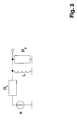
- the known circuit for measuring distances is designed as a discrete circuit and has two inputs 1, 2 and a measuring coil 3.
- two input signals e pos and e neg are generated.
- the inputs 1, 2 are in this case controlled by means of the input signals e pos and e neg , wherein the input signals e pos and e neg preprocessed applied to the inputs 1, 2 of the measuring coil 3.
- the known AC-excited circuit allows the metrological detection of a DC component, which is proportional to the temperature.
- the inputs 1, 2 subsequent operational amplifier form with their resistors a voltage / current converter.
- the current is coupled from both sides into the measuring coil 3.
- the in Fig. 2a shown AC input signals e pos and e neg used to control the inputs.
- the in Fig. 2b shown input signals e pos and e neg used.
- the input 1 associated operation amplifier 5 connected to the resistors R 2, R 3 and the capacitance C 2 has a low-pass behavior and the input 2 associated operational amplifier 6 in conjunction with resistors R 1 , R 3 and the capacitances C 1 and C 2 has a bandpass behavior.
- the overall transfer function is a low-pass function, which is smoothed by the capacitance C 2 .
- the low pass results from the difference between a high pass and a gain path matched with it.
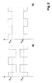
- Fig. 3 shows an equivalent passive double-resistive reference network of a high-pass circuit. It consists of a voltage source e, a voltage divider of the resistors R 1 and R 2 and an inductor L connected in parallel with the resistor R 2.
- the wave flux diagram comprises a three-parallel adapter 7, in which the different characteristic impedances of the three components of the Fig. 3 be adapted to each other.
- p becomes j ⁇ and thus ⁇ ⁇ tan .omega.t 2 ,
- This technique describes different ways of implementing wave-switch-capacitor-filters - SC-filters.
- Fig. 5 shows an inventive SC implementation of the high-pass circuit.
- the circuit has an SC network, with an SC amplifier 8 serving to simulate equation 13.
- the input signal e pos and the input signal b 2 * of the SC amplifier 8 are positively delayed and multiplied according to equation 13 with the coefficients ⁇ 1 and ⁇ 2 .
- the output of the SC amplifier 8 is simultaneously the output of the high-pass circuit.
- Equation 13 Since the output voltage according to equation 15 results as the arithmetic mean of the incident and the reflected voltage wave, the 0dB level is reached at the output because the division with the factor two is not performed.
- the two coefficients of Equation 13 are modeled as capacitance ratios in the signal paths.
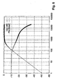
- the realization of equation 13 and equation 15 is formed by a non-delayed negative SC integrator 9. By coupling the output signal of the SC integrator 9 into the SC amplifier 8 in phase ⁇ , the feedback loop is closed. The transfer function of this high-pass circuit is in Fig. 6 shown. Clearly recognizable here is the time-discrete high-pass function of the high-pass circuit.
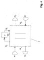
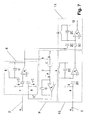
- FIG. 7 An inventive circuit for measuring distances is in Fig. 7 shown.
- the circuit comprises two inputs 1, 2, a - not shown here - signal source and a - also not shown - measuring coil.
- the inputs 1, 2 are controlled by means of two generated by the signal source input signals e pos and e neg .
- the input signals e pos and e neg are applied to a clocked SC network and serve to generate a measurement signal and / or an output signal U.
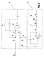
- the circuit also includes an SC amplifier 10, with the input signal e neg at the same instant at the output of the operational amplifier of the SC amplifier 10 as the SC amplifier 8 provides the output signal at the operational amplifier.
- the timing of the SC amplifier 10 is also with the Clocking of the upper SC amplifier 8 identical.
- the input signal e neg is delayed positive by half a clock period to the output.
- the SC network has an SC adder 11 which serves to add the two input signals, ie the output signals of the SC amplifiers 8 and 10.
- the SC network is a positive delay SC circuit, which has a total delay of one clock period. If this is too high, also the input amplifiers and the output amplifier could not be realized negatively delayed. The SC integrator must then be implemented with positive delay. In this case, the output signal is inverted.
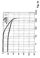
- Fig. 8 shows the transfer function of the circuit of Fig. 9 . It can be clearly seen that the SC network has a low-pass behavior and is therefore very well suited for DC voltage measurement.
- the output voltage of the high-pass filter is the voltage across the resistor R 2 or the voltage across the inductance L, since both elements are connected in parallel.
- the output voltage results as the difference of the incident wave a 2 and the negative reflected wave b 2 divided by 2. Without the division one again obtains a maximum level of 0 dB, which is why the signal can be added back to the input signal e neg .
- FIG. 9 A circuit that realizes this is shown in FIG.
- the circuit comprises a positive delayed SC amplifier 12, a lossy SC integrator 13 and an SC differential amplifier 14.
- the factor (1- ⁇ 2 ) can be obtained as in Fig. 9 can be seen through the lossy SC integrator 13 realize.
- ⁇ 2 is smaller than 1
- the integrator capacity of the size (1- ⁇ 2 ) C is used and in parallel a capacity of the size ⁇ 2 C is switched, which is periodically discharged.
- ⁇ 2 is always less than 1. Since the output value at the SC integrator 13 should always be positive, the input signal e pos positively delayed multiplied by ⁇ 1 .
- the output voltage of the high-pass filter is generated by means of the SC differential amplifier 14. With the input capacitance for the lossy integrator 13, the difference a 2 - b 2 is generated.
- the SC differential amplifier 14 is initialized with ⁇ and the output signal U is thus inverted.
- the second input signal e neg is, as already, with respect to Fig. 7 is applied to the SC amplifier 12 and forwarded to the SC differential amplifier 14.
- the transfer function of in Fig. 9 shown circuit is in Fig. 10 displayed. It can be seen that, apart from a phase shift of 180 °, there is no change compared to the transfer function in Fig. 8 can be observed. Due to the good matching properties of the circuits, the measured DC output signal U is very well suited for temperature correction.
Landscapes
- Physics & Mathematics (AREA)
- General Physics & Mathematics (AREA)
- Transmission And Conversion Of Sensor Element Output (AREA)
- Amplifiers (AREA)
Applications Claiming Priority (3)
| Application Number | Priority Date | Filing Date | Title |
|---|---|---|---|
| DE10146287 | 2001-09-19 | ||
| DE10146287 | 2001-09-19 | ||
| PCT/DE2002/003507 WO2003027613A1 (de) | 2001-09-19 | 2002-09-19 | Schaltung zur messung von wegstrecken |
Publications (2)
| Publication Number | Publication Date |
|---|---|
| EP1427996A1 EP1427996A1 (de) | 2004-06-16 |
| EP1427996B1 true EP1427996B1 (de) | 2010-11-17 |
Family
ID=7699625
Family Applications (1)
| Application Number | Title | Priority Date | Filing Date |
|---|---|---|---|
| EP02774385A Expired - Lifetime EP1427996B1 (de) | 2001-09-19 | 2002-09-19 | Schaltung zur messung von wegstrecken |
Country Status (5)
| Country | Link |
|---|---|
| US (1) | US7061230B2 (enExample) |
| EP (1) | EP1427996B1 (enExample) |
| JP (2) | JP2005504286A (enExample) |
| DE (2) | DE50214778D1 (enExample) |
| WO (1) | WO2003027613A1 (enExample) |
Families Citing this family (33)
| Publication number | Priority date | Publication date | Assignee | Title |
|---|---|---|---|---|
| DE10348343B3 (de) * | 2003-10-17 | 2005-02-03 | Knorr-Bremse Systeme für Nutzfahrzeuge GmbH | Schaltungsanordnung zur induktiven Wegmessung |
| WO2010045662A2 (en) | 2008-10-15 | 2010-04-22 | Azoteq (Pty) Ltd | Parasitic capacitance cancellation in capacitive measurement applications |
| US20140002069A1 (en) * | 2012-06-27 | 2014-01-02 | Kenneth Stoddard | Eddy current probe |
| WO2014197611A1 (en) * | 2013-06-04 | 2014-12-11 | Eagle Harbor Technologies, Inc. | Analog integrator system and method |
| US9655221B2 (en) | 2013-08-19 | 2017-05-16 | Eagle Harbor Technologies, Inc. | High frequency, repetitive, compact toroid-generation for radiation production |
| US10892140B2 (en) | 2018-07-27 | 2021-01-12 | Eagle Harbor Technologies, Inc. | Nanosecond pulser bias compensation |
| US10020800B2 (en) | 2013-11-14 | 2018-07-10 | Eagle Harbor Technologies, Inc. | High voltage nanosecond pulser with variable pulse width and pulse repetition frequency |
| US10978955B2 (en) | 2014-02-28 | 2021-04-13 | Eagle Harbor Technologies, Inc. | Nanosecond pulser bias compensation |
| CN116633324A (zh) | 2013-11-14 | 2023-08-22 | 鹰港科技有限公司 | 高压纳秒脉冲发生器 |
| US9706630B2 (en) | 2014-02-28 | 2017-07-11 | Eagle Harbor Technologies, Inc. | Galvanically isolated output variable pulse generator disclosure |
| US11539352B2 (en) | 2013-11-14 | 2022-12-27 | Eagle Harbor Technologies, Inc. | Transformer resonant converter |
| US10790816B2 (en) | 2014-01-27 | 2020-09-29 | Eagle Harbor Technologies, Inc. | Solid-state replacement for tube-based modulators |
| US10483089B2 (en) | 2014-02-28 | 2019-11-19 | Eagle Harbor Technologies, Inc. | High voltage resistive output stage circuit |
| WO2016138546A2 (en) | 2015-02-27 | 2016-09-01 | Azoteq (Pty) Ltd | Inductance sensing |
| US11542927B2 (en) | 2015-05-04 | 2023-01-03 | Eagle Harbor Technologies, Inc. | Low pressure dielectric barrier discharge plasma thruster |
| US10903047B2 (en) | 2018-07-27 | 2021-01-26 | Eagle Harbor Technologies, Inc. | Precise plasma control system |
| US11430635B2 (en) | 2018-07-27 | 2022-08-30 | Eagle Harbor Technologies, Inc. | Precise plasma control system |
| US11004660B2 (en) | 2018-11-30 | 2021-05-11 | Eagle Harbor Technologies, Inc. | Variable output impedance RF generator |
| EP3580841A4 (en) | 2017-02-07 | 2020-12-16 | Eagle Harbor Technologies, Inc. | TRANSFORMER-RESONANCE CONVERTER |
| JP6902167B2 (ja) | 2017-08-25 | 2021-07-14 | イーグル ハーバー テクノロジーズ, インク.Eagle Harbor Technologies, Inc. | ナノ秒パルスを使用する任意波形の発生 |
| US11302518B2 (en) | 2018-07-27 | 2022-04-12 | Eagle Harbor Technologies, Inc. | Efficient energy recovery in a nanosecond pulser circuit |
| US11810761B2 (en) | 2018-07-27 | 2023-11-07 | Eagle Harbor Technologies, Inc. | Nanosecond pulser ADC system |
| US11532457B2 (en) | 2018-07-27 | 2022-12-20 | Eagle Harbor Technologies, Inc. | Precise plasma control system |
| US10607814B2 (en) | 2018-08-10 | 2020-03-31 | Eagle Harbor Technologies, Inc. | High voltage switch with isolated power |
| US11222767B2 (en) | 2018-07-27 | 2022-01-11 | Eagle Harbor Technologies, Inc. | Nanosecond pulser bias compensation |
| KR102499709B1 (ko) | 2018-08-10 | 2023-02-16 | 이글 하버 테크놀로지스, 인코포레이티드 | RF 플라즈마 반응기용 플라즈마 시스(sheath) 제어 |
| WO2021134000A1 (en) | 2019-12-24 | 2021-07-01 | Eagle Harbor Technologies, Inc. | Nanosecond pulser rf isolation for plasma systems |
| US12456604B2 (en) | 2019-12-24 | 2025-10-28 | Eagle Harbor Technologies, Inc. | Nanosecond pulser RF isolation for plasma systems |
| US10796887B2 (en) | 2019-01-08 | 2020-10-06 | Eagle Harbor Technologies, Inc. | Efficient nanosecond pulser with source and sink capability for plasma control applications |
| TWI778449B (zh) | 2019-11-15 | 2022-09-21 | 美商鷹港科技股份有限公司 | 高電壓脈衝電路 |
| US11967484B2 (en) | 2020-07-09 | 2024-04-23 | Eagle Harbor Technologies, Inc. | Ion current droop compensation |
| US11824542B1 (en) | 2022-06-29 | 2023-11-21 | Eagle Harbor Technologies, Inc. | Bipolar high voltage pulser |
| KR20250084155A (ko) | 2022-09-29 | 2025-06-10 | 이글 하버 테크놀로지스, 인코포레이티드 | 고전압 플라즈마 제어 |
Family Cites Families (12)
| Publication number | Priority date | Publication date | Assignee | Title |
|---|---|---|---|---|
| DE3543935A1 (de) * | 1985-12-12 | 1987-06-19 | Siemens Ag | Induktiver naeherungsschalter |
| US5148166A (en) * | 1990-04-06 | 1992-09-15 | General Electric Company | Third order sigma delta oversampled analog-to-digital converter network with low component sensitivity |
| DE4017843A1 (de) * | 1990-06-02 | 1991-12-05 | Bosch Gmbh Robert | Sensorschaltung |
| JP3337241B2 (ja) * | 1991-07-26 | 2002-10-21 | テキサス インスツルメンツ インコーポレイテツド | 改良型多重チャンネル・センサーインターフェース回路とその製造方法 |
| DE4225968A1 (de) * | 1992-08-06 | 1994-02-10 | Micro Epsilon Messtechnik | Berührungslos arbeitendes Wegmeßsystem und Verfahren zur berührungslosen Wegmessung |
| JP3302826B2 (ja) * | 1994-05-20 | 2002-07-15 | 三菱電機株式会社 | センサ駆動回路 |
| US5712563A (en) * | 1994-06-13 | 1998-01-27 | Honda Giken Kogyo Kabushiki Kaisha | Steering torque sensor utilizing a displacement detector having a pulse power supply |
| US5729163A (en) * | 1994-10-18 | 1998-03-17 | The Boeing Company | Synchronous AC to DC conversion of differential AC signals |
| WO1998059216A1 (de) * | 1997-06-21 | 1998-12-30 | Micro-Epsilon Messtechnik Gmbh & Co. Kg | Wirbelstromsensor |
| US6073043A (en) * | 1997-12-22 | 2000-06-06 | Cormedica Corporation | Measuring position and orientation using magnetic fields |
| JP2967413B1 (ja) * | 1998-04-20 | 1999-10-25 | 株式会社千葉精密 | 回転差動容量型角度変換器 |
| SG104277A1 (en) * | 2001-09-24 | 2004-06-21 | Inst Of Microelectronics | Circuit for measuring changes in capacitor gap using a switched capacitor technique |
-
2002
- 2002-09-19 JP JP2003531122A patent/JP2005504286A/ja active Pending
- 2002-09-19 EP EP02774385A patent/EP1427996B1/de not_active Expired - Lifetime
- 2002-09-19 DE DE50214778T patent/DE50214778D1/de not_active Expired - Lifetime
- 2002-09-19 WO PCT/DE2002/003507 patent/WO2003027613A1/de not_active Ceased
- 2002-09-19 DE DE10243631A patent/DE10243631A1/de not_active Ceased
-
2004
- 2004-03-18 US US10/803,298 patent/US7061230B2/en not_active Expired - Fee Related
-
2008
- 2008-06-09 JP JP2008150873A patent/JP4796605B2/ja not_active Expired - Fee Related
Also Published As
| Publication number | Publication date |
|---|---|
| US7061230B2 (en) | 2006-06-13 |
| DE50214778D1 (de) | 2010-12-30 |
| US20040201376A1 (en) | 2004-10-14 |
| DE10243631A1 (de) | 2003-04-24 |
| WO2003027613A1 (de) | 2003-04-03 |
| EP1427996A1 (de) | 2004-06-16 |
| JP4796605B2 (ja) | 2011-10-19 |
| JP2005504286A (ja) | 2005-02-10 |
| JP2008275634A (ja) | 2008-11-13 |
Similar Documents
| Publication | Publication Date | Title |
|---|---|---|
| EP1427996B1 (de) | Schaltung zur messung von wegstrecken | |
| EP3335012B1 (de) | Elektronische steuerungseinheit | |
| DE69425160T2 (de) | Vorrichtung zur messung von materialeigenschaft | |
| EP0503272B1 (de) | Schaltungsanordnung zur Messung des Quotienten der Kapazitätswerte zweier Kondensatoren | |
| DE102011078334A1 (de) | Verfahren und System zum Kalibrieren eines Shunt-Widerstands | |
| DE102012218773A1 (de) | Verfahren und Einrichtung zur Messung eines Stroms durch einen Schalter | |
| DE19849910A1 (de) | Offsetkompensiertes Winkelmeßsystem | |
| EP0813306A1 (de) | Temperaturstabilisierter Oszillator und Verwendung desselben in einem Näherungsschalter | |
| EP3293499B1 (de) | Verfahren zum betreiben eines magnetisch-induktiven durchflussmessgeräts und magnetisch-induktives durchflussmessgerät | |
| CH698425B1 (de) | Anordnung zum Messen einer physikalischen Grösse. | |
| DE2059728A1 (de) | Spulenloser Daempfungs- und Laufzeitentzerrer | |
| DE3642771C2 (enExample) | ||
| WO2003060482A2 (de) | Vorrichtung zur messung der viskosität und/oder der dichte | |
| EP2033310B1 (de) | Temperaturstabilisierter schwingkreis für induktive sensoren | |
| EP1960740A1 (de) | Induktiver positionssensor | |
| DE3709532A1 (de) | Verfahren zur pruefung von anordnungen | |
| EP1592131B1 (de) | Spektrumanalysator mit hoher Geschwindigkeit und gleichzeitig hoher Auflösung | |
| EP0489259A2 (de) | Kapazitäts-Frequenz-Wandler | |
| WO2003076956A2 (de) | Verfahren zum messen der effektiven direktivität und/oder effektiven quelltor-anpassung eines systemkalibrierten vektoriellen netzwerkanalysators | |
| DE2534509A1 (de) | Signalverarbeitungs-verfahren und -anordnung | |
| DE2460079C3 (de) | Verfahren zur Bestimmung der Stellung des Schleifers eines Potentiometers und Schaltungsanordnung zur Durchführung des Verfahrens | |
| DE3927833C2 (de) | Meßschaltung und Anwendung derselben, insbesondere mit induktiven Weggebern | |
| EP1427997A1 (de) | Schaltung zur demodulation | |
| DE3642495C2 (enExample) | ||
| EP1091214B1 (de) | Verfahren und Vorrichtung zur Aufbereitung von Messsignalen |
Legal Events
| Date | Code | Title | Description |
|---|---|---|---|
| PUAI | Public reference made under article 153(3) epc to a published international application that has entered the european phase |
Free format text: ORIGINAL CODE: 0009012 |
|
| 17P | Request for examination filed |
Effective date: 20040205 |
|
| AK | Designated contracting states |
Kind code of ref document: A1 Designated state(s): AT BE BG CH CY CZ DE DK EE ES FI FR GB GR IE IT LI LU MC NL PT SE SK TR |
|
| RIN1 | Information on inventor provided before grant (corrected) |
Inventor name: ROEWER, FALK Inventor name: MEDNIKOV, FELIX Inventor name: SELLEN, MARTIN Inventor name: SALZWEDEL, KLAUS Inventor name: KLEINE, ULRICH |
|
| GRAP | Despatch of communication of intention to grant a patent |
Free format text: ORIGINAL CODE: EPIDOSNIGR1 |
|
| RBV | Designated contracting states (corrected) |
Designated state(s): DE FR GB |
|
| GRAS | Grant fee paid |
Free format text: ORIGINAL CODE: EPIDOSNIGR3 |
|
| GRAA | (expected) grant |
Free format text: ORIGINAL CODE: 0009210 |
|
| AK | Designated contracting states |
Kind code of ref document: B1 Designated state(s): DE FR GB |
|
| REG | Reference to a national code |
Ref country code: GB Ref legal event code: FG4D Free format text: NOT ENGLISH |
|
| REF | Corresponds to: |
Ref document number: 50214778 Country of ref document: DE Date of ref document: 20101230 Kind code of ref document: P |
|
| PLBE | No opposition filed within time limit |
Free format text: ORIGINAL CODE: 0009261 |
|
| STAA | Information on the status of an ep patent application or granted ep patent |
Free format text: STATUS: NO OPPOSITION FILED WITHIN TIME LIMIT |
|
| 26N | No opposition filed |
Effective date: 20110818 |
|
| REG | Reference to a national code |
Ref country code: DE Ref legal event code: R097 Ref document number: 50214778 Country of ref document: DE Effective date: 20110818 |
|
| PGFP | Annual fee paid to national office [announced via postgrant information from national office to epo] |
Ref country code: GB Payment date: 20120920 Year of fee payment: 11 |
|
| PGFP | Annual fee paid to national office [announced via postgrant information from national office to epo] |
Ref country code: FR Payment date: 20121008 Year of fee payment: 11 Ref country code: DE Payment date: 20121129 Year of fee payment: 11 |
|
| GBPC | Gb: european patent ceased through non-payment of renewal fee |
Effective date: 20130919 |
|
| REG | Reference to a national code |
Ref country code: DE Ref legal event code: R119 Ref document number: 50214778 Country of ref document: DE Effective date: 20140401 |
|
| REG | Reference to a national code |
Ref country code: FR Ref legal event code: ST Effective date: 20140530 |
|
| PG25 | Lapsed in a contracting state [announced via postgrant information from national office to epo] |
Ref country code: GB Free format text: LAPSE BECAUSE OF NON-PAYMENT OF DUE FEES Effective date: 20130919 |
|
| PG25 | Lapsed in a contracting state [announced via postgrant information from national office to epo] |
Ref country code: DE Free format text: LAPSE BECAUSE OF NON-PAYMENT OF DUE FEES Effective date: 20140401 Ref country code: FR Free format text: LAPSE BECAUSE OF NON-PAYMENT OF DUE FEES Effective date: 20130930 |