FIELD OF THE INVENTION
-
The present invention relates to a thin metal
layers-having ceramic green sheet, and a method for
producing a ceramic capacitor. More particularly, the
invention relates to a thin metal layers-having ceramic
green sheet suitably used for the production of a ceramic
capacitor, and a method for producing a ceramic capacitor
using the thin metal layers-having ceramic green sheet.
BACKGROUND OF THE INVENTION
-
As a method for producing a ceramic capacitor, for
example, Japanese Patent Nos. 2,990,621, 2,970,238, etc.
disclose a method for producing a laminated ceramic
capacitor having a thin metal layer of a predetermined
pattern as an internal electrode by forming a thin metal
layer in a predetermined pattern on a base film, forming a
ceramic green sheet on the thin metal layer-containing
base film surface so as to cover the thin metal layer,
thereby forming a ceramic green sheet having the thin
metal layer supported on the base film, subsequently,
forming a laminate of a plurality of the thus obtained
ceramic green sheets having the thin metal layers by
sequentially superposing one on another after peeling the
base film for each superposition, and then burning the
resulting laminate.
-
More specifically, Japanese Patent No. 2,990,621
discloses a method for producing a laminated ceramic
electronic component comprising ceramic green sheets and
electrodes formed on the surfaces of the ceramic green
sheets, which comprises the steps of (a) forming a first
metal layer on a film by vapor deposition, (b) forming a
second metal layer on the first metal layer by wet plating,
(c) patterning the first and second metal layers, (d)
coating the film with a ceramic slurry so as to cover the
metal layers to form a ceramic green sheet, (e) press-bonding
the metal-integrated green sheet supported on the
film onto a ceramic green sheet or another metal-integrated
green sheet to perform lamination, (f) peeling
the film, and (g) burning the laminated ceramic green
sheet.
-
Further, Japanese Patent No. 2,970,238 discloses a
method for producing a laminated ceramic capacitor, which
comprises: a first step of forming a metal film having a
predetermined pattern on a base film by a thin film
forming process; a second step of forming a ceramic
dielectric layer on the base film so as to cover the metal
film to prepare a green sheet having the base film; a
third step of superposing the green sheet having the base
film onto a dielectric sheet so that the dielectric sheet
comes into contact with the ceramic dielectric layer of
the green sheet having the base film, and then peeling the
base film; a fourth step of superposing another green
sheet having a base film obtained by the first step and
the second step onto the green sheet obtained by the third
step so that the ceramic dielectric layer of the former
comes into contact with the latter, and then peeling the
base film of the former in order to further perform
lamination; a fifth step of repeating the operation of the
fourth step in the same manner predetermined times to
obtain a laminated green sheet; a sixth step of cutting
the thus obtained green sheet to prepare a chip and
burning the chip; and a seventh step of forming an
external electrode on the chip.
-
However, at the time of burning the laminated
ceramic green sheets in the above-mentioned methods, a
binder in each ceramic green sheet disappears to cause
contraction over the whole ceramic green sheet. At this
time, a portion in which a thin metal layer serveing as an
internal electrode is formed has a different contraction
percentage from a portion in which no thin metal layer is
formed, which causes non-uniform contraction to induce
strain over the whole ceramic green sheet. This sometimes
results in separation between the internal electrode and
an insulating layer, separation between upper and lower
insulating layers or occurrence of internal cracks in the
insulating layer in the resulting laminated ceramic
capacitor.
-
Further, when the ceramic green sheet is formed on
the base film, a slurry for the ceramic green sheet is
first applied onto the base film. However, the slurry may
sometime be repelled on a surface of the base film,
resulting in failure to obtain a uniform coating, because
the wettability of the slurry to the surface of the base
film is low.
-
Furthermore, in the case where a mask film is formed
on the base film for forming the thin metal layer, the
formation of the thin metal layer may run over a
predetermined wiring circuit pattern unless the adhesion
between the base film and the mask film is sufficient.
SUMMARY OF THE INVENTION
-
The invention has been made in view of the
circumstances as described above.
-
Accordingly, an object of the invention is to
provide a thin metal layers-having ceramic green sheet
which uniformly contracts upon burning a laminated ceramic
powder-dispersed layer so as to prevent the separation
between an internal electrode and an insulating layer, the
separation between upper and lower insulating layers or
the occurrence of internal cracks in the insulating layer,
in which the ceramic powder-dispersed layer is uniformly
formed, and further in which the thin metal layer is
formed as a high-precision pattern.
-
Another object of the invention is to provide a
method for producing a ceramic capacitor using the thin
metal layers-having ceramic green sheet.
-
Other objects and effects of the invention will
become apparent from the following description.
-
In order to achieved the above-described objects,
the present invention provides a thin metal layers-having
ceramic green sheet comprising:
- a base film;
- a first thin metal layer formed on the whole surface
of said base film;
- a second thin metal layer formed on said first thin
metal layer in the form of predetermined pattern; and
- a ceramic powder-dispersed layer, comprising a
binder and a ceramic powder dispersed therein, and being
formed on the first thin metal layer surface including the
second thin metal layer surface.
-
-
According to such thin metal layers-having ceramic
green sheets, when they are used in the production of a
ceramic capacitor and the whole ceramic powder-dispersed
layers contract due to disappearance of the binder
contained therein upon burning a laminate obtained by
stacking the ceramic green sheets, an uniform contraction
percentage can be assured by the respective first thin
metal layers intervening between the neighboring ceramic
powder-dispersed layers over the whole surfaces thereof,
thereby allowing the whole ceramic powder-dispersed layers
to contract uniformly. Accordingly, the separation
between the internal electrode and the insulating layer,
the separation between the upper and lower insulating
layers or the occurrence of internal cracks in the
insulating layer, caused by a non-uniform contraction can
be effectively prevented.
-
Further, the ceramic powder-dispersed layer is
formed on the first thin metal layer surface including the
second thin metal layer surface, not on the base film.
Accordingly, for example, when the ceramic powder-dispersed
layer is formed by applying a slurry therefor
onto the first thin metal layer surface including the
second thin metal layer surface in the production of the
thin metal layers-having ceramic green sheet, good
wettability between the slurry and the first thin metal
layer surface including the second thin metal layer
surface makes it possible to form the ceramic powder-dispersed
layer uniformly.
-
Still further, the second thin metal layer is formed
on the first thin metal layer, not on the base film.
Accordingly, for example, when the second thin metal layer
is formed in the form of predetermined pattern by use of a
mask film, good adhesion can be assured between the first
thin metal layer and the mask film to thereby form the
second thin metal layer as a high-precision pattern.
-
Furthermore, in the invention, it is preferred that
a resin layer is provided between the base film and the
first thin metal layer.
-
When the resin layer is provided between the base
film and the first thin metal layer, the first thin metal
layer including the second thin metal layer can be formed
on the resin layer, not on the base film. Accordingly,
when the base film is peeled in the production of the
ceramic capacitor, the base film can be peeled at an
interface with the resin layer, so that damages of the
first thin metal layer including the second thin metal
layer upon peeling the base film can be prevented.
-
Further, in the invention, it is preferred that the
resin layer comprises a material substantially the same as
the binder of the ceramic powder-dispersed layer.
-
In the case where the resin layer is constituted by
a material substantially the same as the binder of the
ceramic powder-dispersed layer, the resin layer material
can be allowed to disappear under the same conditions as
those for the binder at the time of burning a laminate
obtained by stacking the thin metal layers-having ceramic
green sheets in the production of the ceramic capacitor.
-
Further, it is preferred that the first thin metal
layer has a thickness of 0.001 to 1.0 µm.
-
When the first thin metal layer has a thickness of
0.001 to 1.0 µm, a portion of the first thin metal layer
on which the second thin metal layer is not formed can be
surely spheroidized or segmentalized at the time of
burning a laminate obtained by stacking the thin metal
layers-having ceramic green sheets in the production of
the ceramic capacitor. Accordingly, the continuity caused
by the first thin metal layer can be surely prevented, and
the sure continuity of the second thin metal layer formed
in the form of predetermined pattern can be ensured. Thus,
the reliability of the ceramic capacitor using the thin
metal layers-having ceramic green sheets can be improved.
-
Further, in the invention, it is preferred that the
thickness of the second thin metal layer is twice or more
that of the first thin metal layer.
-
When the thickness of the second thin metal layer is
less than twice that of the first thin metal layer, the
spheroidizing or segmentalization of the first thin metal
layer may become predominant at the time of burning a
laminate obtained by stacking the thin metal layers-having
ceramic green sheets in the production of the ceramic
capacitor, to thereby cause damage to the second thin
metal layer. However, when the thickness of the second
thin metal layer is twice or more that of the first thin
metal layer, such damage can be prevented to ensure the
sure formation of the internal electrode.
-
Further, the invention also provides a method for
producing a ceramic capacitor comprising the steps of:
- preparing a plurality of the above-described thin
metal layers-having ceramic green sheets;
- peeling the base film of one of said plurality of
thin metal layers-having ceramic green sheets;
- superposing another thin metal layers-having ceramic
green sheet on said base film-peeled ceramic green sheet
by bringing the ceramic powder-dispersed layer of said
another ceramic green sheet into contact with the first
thin metal layer or resin layer of said base film-peeled
ceramic green sheet;
- repeating said peeling step and said superposing
step predetermined times to form a laminated product of
said plurality of ceramic green sheets; and
- burning said laminated product.
-
-
According to such a method for producing the ceramic
capacitor, the whole ceramic powder-dispersed layers can
be allowed to contract uniformly in the step of burning
the laminate of the thin metal layers-having ceramic green
sheets, because the thin metal layers-having ceramic green
sheets of the invention are used. Accordingly, the
separation between the internal electrode and the
insulating layer, the separation between the upper and
lower insulating layers or the occurrence of internal
cracks in the insulating layer, caused by the non-uniform
contraction can be effectively prevented, thus making it
possible to produce the ceramic capacitor having high
reliability.
BRIEF DESCRIPTION OF THE DRAWINGS
-
- Figs. 1 constitute a flow chart showing one
embodiment of a method for producing one example of the
thin metal layers-having ceramic green sheet of the
invention, wherein:
- Fig. 1(a) indicates the step of preparing a base
film;
- Fig. 1(b) indicates the step of forming a resin
layer on the base film;
- Fig. 1(c) indicates the step of forming a first thin
metal layer on the whole surface of the rein layer;
- Fig. 1(d) indicates the step of forming a second
thin metal layer on the first thin metal layer in the form
of a predetermined wiring circuit pattern; and
- Fig. 1(e) indicates the step of forming a ceramic
powder-dispersed layer on the first thin metal layer
surface including the second thin metal layer surface.
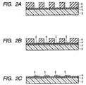
- Figs. 2 constitute a flow chart showing one
embodiment of the step of forming the second thin metal
layer on the first thin metal layer in the form of the
predetermined wiring circuit pattern, which is indicated
by Fig. 1(d), in the production method of the thin metal
layers-having ceramic green sheet shown in Figs. 1,
wherein:
- Fig. 2(a) indicates the step of forming a plating
resist on the first thin metal layer in a pattern reverse
to the wiring circuit pattern;
- Fig. 2(b) indicates the step of forming the second
thin metal layer by plating on the first thin metal layer
exposed from the plating resist as the wiring circuit
pattern; and
- Fig. 2(c) indicates the step of removing the plating
resist.
- Figs. 3 constitute a flow chart showing one
embodiment of the production method of a ceramic capacitor
of the invention, wherein:
- Fig. 3(a) indicates the step of peeling a base film
of a first ceramic green sheet having thin metal layers;
- Fig. 3(b) indicates the step of superposing a second
ceramic green sheet having thin metal layers on the first
ceramic green sheet having thin metal layers so that the
surface of the ceramic powder-dispersed layer of the
second ceramic green sheet having thin metal layers comes
into contact with the surface of the resin layer of the
first ceramic green sheet having thin metal layers;
- Fig. 3(c) indicates the step of peeling the base
film of the second ceramic green sheet having thin metal
layers,
- Fig. 3(d) indicates the step of stacking a desired
number of thin metal layers-having ceramic green sheets;
and
- Fig. 3(e) indicates the step of burning.
- Fig. 4 is a schematic cross sectional view showing
one embodiment of a laminated ceramic capacitor obtained
by the production method of the ceramic capacitor shown in
Fig. 3.
- Figs. 5 constitute a flow chart showing one
embodiment of a method for producing another example of
the thin metal layers-having ceramic green sheet of the
invention, wherein:
- Fig. 5(a) indicates the step of preparing a base
film;
- Fig. 5(b) indicates the step of forming a first thin
metal layer on the whole surface of the base film;
- Fig. 5(c) indicates the step of forming a second
thin metal layer on the first thin metal layer in the form
of a predetermined wiring circuit pattern; and
- Fig. 5(d) indicates the step of forming a ceramic
powder-dispersed layer on the first thin metal layer
surface including the second thin metal layer surface.
- Figs. 6 constitute a flow chart showing the method
for producing the thin metal layers-having ceramic green
sheet of Comparative Example 1, wherein:
- Fig. 6(a) indicates the step of preparing a base
film;
- Fig. 6(b) indicates the step of forming a first thin
metal layer on the whole surface of the base film;
- Fig. 6(c) indicates the step of forming a second
thin metal layer on the first thin metal layer in the form
of a predetermined wiring circuit pattern;
- Fig. 6(d) indicates the step of processing the first
thin metal layer into the form of the predetermined wiring
circuit pattern; and
- Fig. 6(e) indicates the step of forming a ceramic
powder-dispersed layer on the base film surface containing
the second thin metal layer surface.
- Figs. 7 constitute a flow chart showing the method
for producing the thin metal layers-having ceramic green
sheet of Comparative Example 2, wherein:
- Fig. 7(a) indicates the step of preparing a base
film;
- Fig. 7(b) indicates the step of forming a resin
layer on the base film;
- Fig. 7(c) indicates the step of forming a first thin
metal layer on the whole surface of the resin layer;
- Fig. 7(d) indicates the step of forming a second
thin metal layer on the first thin metal layer in the form
of a predetermined wiring circuit pattern;
- Fig. 7(e) indicates the step of processing the first
thin metal layer into the form of the predetermined wiring
circuit pattern; and
- Fig. 7(f) indicates the step of forming a ceramic
powder-dispersed layer on the resin layer surface
including the second thin metal layers surface.
-
DETAILED DESCRIPTION OF THE INVENTION
-
Figs. 1 constitute a flow chart showing one
embodiment of a method for producing one example of the
thin metal layers-having ceramic green sheet of the
invention. Referring to Figs. 1, the method for producing
one example of the thin metal layers-having ceramic green
sheet of the invention is described below.
-
First, in this method, a base film 2 is prepared as
shown in Fig. 1(a).
-
There is no particular limitation on the base film 2,
and examples thereof include known plastic films such as a
polyethylene film, a polypropylene film, a polystyrene
film, a polyvinyl chloride film, a polyethylene
terephthalate film, a polycarbonate film, a TPX
(methylpentene resin) film, an alkyd resin film, a
polyimide film, a polysulfone film, a polyethersulfone
film, a polyamide film, a polyamideimide film, a
polyetherketone film and a polyphenylene sulfide film.
Although there is no particular limitation on the
thickness of the base film 2, it is, for example,
preferably from 5 to 500 µm, and more preferably from 10
to 100 µm.
-
As the base film 2, a film having a surface which
has been subjected to a mold releasing treatment is
preferably used. As the mold releasing treatment, a known
mold releasing treatment is preferably used. For example,
a release agent such as a silicone compound, a silicone
fluoride compound, a fluorine-containing compound or a
long-chain alkyd compound can be applied onto the surface
of the base film 2. Incidentally, plastic films having
mold releasability such as polypropylene films or TPX
films may be used as such without any mold releasing
treatment.
-
Then, in this method, a resin layer 3 is formed on
the base film 2 as shown in Fig. 1(b).
-
The resin forming the resin layer 3 is a resin which
disappears at the time of burning a laminate obtained by
stacking the thin metal layers-having ceramic green sheets
1 in the production of a ceramic capacitor 11 described
later, and is not particularly limited as long as it is a
resin having good release properties with respect to the
base film 2. Examples thereof include cellulose resins
such as ethyl cellulose, hydroxypropyl cellulose and
carboxymethyl cellulose, acrylic resins such as butyl
methacrylate and methyl methacrylate, polyvinyl butyral
resins, polyvinyl alcohol resins, vinyl acetate resins and
urethane resins.
-
These resins can be used either alone or as a
combination of two or more thereof.
-
Further, the resin forming the resin layer 3 is
preferably the same material as the binder of the ceramic
powder-dispersed layer 7 described later. When the resin
is the same material as the binder of the ceramic powder-dispersed
layer 7, it can be allowed to disappear under
the same conditions as those for the binder at the time of
burning the laminate obtained by stacking the thin metal
layers-having ceramic green sheets 1 in the production of
the ceramic capacitor 11.
-
There is no particular limitation on the method of
forming the resin layer 3 on the base film 2. For example,
the resin layer can be formed by preparing a solution of
the resin, applying the solution onto the base film 2, and
drying the applied solution.
-
There is no particular limitation on the method of
preparing the solution of the resin. For example, the
above-mentioned resin may be dissolved in a solvent that
is the same as or similar to a dispersing medium for the
binder described later so as to give a resin concentration
(solid concentration) of 1 to 50% by weight, preferably 3
to 30% by weight.
-
Further, for coating the solution of the resin,
known methods such as spin coating, doctor blade coating
and spray coating can be used.
-
The drying temperature after coating can be
appropriately selected depending on the type of the resin
or solvent and is, for example, from 40 to 200°C, and
preferably from 60 to 150°C.
-
The thickness of the resin layer 3 thus formed is,
for example, preferably from 0.1 to 1.0 µm, and more
preferably from 0.1 to 0.5 µm. When the thickness of the
resin layer 3 is within such a range, the good release
properties of the base film 2 can be ensured.
-
Then, in this method, a first thin metal layer 4 is
formed on the whole surface of the resin layer 3.
-
There is no particular limitation on the metal
forming the first thin metal layer 4, as long as it is a
metal used as an internal electrode of the laminated
ceramic capacitor 11, and examples thereof include copper,
nickel, chromium, palladium or alloys thereof.
-
Although there is no particular limitation on the
method of forming the first thin metal layer 4 on the
resin layer 3, for example, vacuum film formation such as
vacuum deposition, ion plating or sputtering can be used.
When the first thin metal layer 4 is formed by the vacuum
film formation, a portion of the first thin metal layer 4
on which the second thin metal layer 5 is not formed (a
portion composed of the first thin metal layer 4 alone)
can be surely spheroidized or segmentalized, for example,
to a particle size of about 1 nm to about 10 µm, at the
time of burning the laminate obtained by stacking the thin
metal layers-having ceramic green sheets 1 in the
production of the laminated ceramic capacitor 11.
-
The thickness of the first thin metal layer 4 thus
formed is, for example, preferably from 0.001 to 1.0 µm,
and more preferably from 0.05 to 0.2 µm. When the
thickness of the first thin metal layer 4 is within such a
range, the first thin metal layer 4 can be surely
spheroidized or segmentalized at the time of burning the
laminate obtained by stacking the thin metal layers-having
ceramic green sheets 1 in the production of the laminated
ceramic capacitor 11.
-
Then, in this method, the second thin metal layer 5
is formed on the first thin metal layer 4 in the form of a
predetermined wiring circuit pattern as shown in Fig. 1(d).
-
There is no particular limitation on the metal
forming the second thin metal layer 5, as long as it is a
metal used as the internal electrode of the laminated
ceramic capacitor 11, and examples thereof include copper,
nickel, chromium, palladium or alloys thereof, similarly
to the first thin metal layer 4. The metal forming the
second thin metal layer 5 may be the same as or different
from the metal forming the first thin metal layer 4.
-
There is no particular limitation on the method of
forming the second thin metal layer 5 in the form of a
predetermined wiring pattern on the first thin metal layer
4. For example, it can be formed by first forming a
plating resist 6 on the first thin metal layer 4 in a
pattern reverse to the wiring circuit pattern, and then
forming the second thin metal layer 5 by plating on the
remaining surface of the first thin metal layer 4 exposed
as the wiring circuit pattern, using the plating resist 6
as a mask, followed by removal of the plating resist 6.
-
More specifically, first, the plating resist 6 is
formed on the first thin metal layer 4 in a pattern
reverse to the wiring circuit pattern (in a reversal
pattern) as shown in Fig. 2(a). There is no particular
limitation on the method of forming the plating resist 6.
For example, a printing method or a dry film method can be
used.
-
Further, although there is no particular limitation
on the thickness of the plating resist 6, it is, for
example, preferably from 1 to 100 µm, and more preferably
from 5 to 25 µm.
-
Then, the second thin metal layer 5 is formed by
plating on the remaining surface of the first thin metal
layer 4 exposed from the plating resist 6 as the wiring
circuit pattern (i.e., the pattern reverse to that of the
plating resist 6), as shown in Fig. 2(b).
-
Although the manner of the plating is not
particularly limited and either electrolytic plating or
non-electrolytic plating may be employed, electrolytic
plating using the first thin metal layer 4 as an electrode
is preferred. If the second thin metal layer 5 is formed
by plating, the temperature at which the spheroidizing or
segmentalization of the second thin metal layer 5 is
initiated becomes higher than that in the case where the
second thin metal layer 5 is formed by the vacuum film
formation. Accordingly, the spheroidizing or
segmentalization of a portion of the first thin metal
layer 4 on which the second thin metal layer 5 is formed
can be prevented at the time of burning the laminate
obtained by stacking the thin metal layers-having ceramic
green sheets 1 in the production of the ceramic capacitor
11.
-
According to the foregoing process for forming the
second thin metal layer 5, the plating resist 6 can be
formed on the first thin metal layer 4, not on the base
film 2, followed by plating, so that the first thin metal
layer 4 can be adhered well to the plating resist 6 to
form the second thin metal layer 5 as a high-precision
wiring circuit pattern.
-
Then, the thickness of the second thin metal layer 5
thus formed in the form of the predetermined wiring
circuit pattern is, for example, preferably from 0.002 to
2.0 µm, and more preferably from 0.1 to 0.6 µm. Further,
the thickness of the second thin metal layer 5 is
preferably twice or more that of the first thin metal
layer 4, and more preferably 3 to 10 times.
-
When the thickness of the second thin metal layer 5
is less than twice that of the first thin metal layer 4,
the spheroidizing or segmentalization of the first thin
metal layer 4 may become predominant at the time of
burning the laminate obtained by stacking the thin metal
layers-having ceramic green sheets 1 in the production of
the ceramic capacitor 11, to thereby cause damages to the
second thin metal layer 5. However, when the thickness of
the second thin metal layer 5 is twice or more that of the
first thin metal layer 4, such damages can be prevented to
ensure the sure formation of the internal electrode.
-
Further, the second thin metal layer 5 can also be
formed to have a multilayer structure of two or more
layers depending on its purpose and use.
-
Then, the plating resist 6 is removed as shown in
Fig. 2(c). There is no particular limitation on the
method of removal of the plating resist 6. For example,
the plating resist 6 can be peeled or etched off.
-
In this method, the ceramic powder-dispersed layer 7
is formed on the surface of the first thin metal layer 4
including the surface of the second thin metal layer 5,
thereby obtaining the thin metal layers-having ceramic
green sheet 1, as shown in Fig. 1(e).
-
There is no particular limitation on the method of
forming the ceramic powder-dispersed layer 7. For example,
it can be formed by preparing a slurry containing at least
ceramic powder and a binder, and applying this slurry onto
the whole surface of the first thin metal layer 4
including the surface of the second thin metal layer 5,
followed by drying.
-
There is no particular limitation on the preparation
method of the slurry, as long as it is a method for
preparing a slurry used in the production of a ceramic
green sheet. For example, it can be prepared by blending
ceramic powder and a binder in a dispersing medium
(solvent), followed by mixing.
-
There is no particular limitation on the ceramic
powder, and examples thereof include dielectric ceramic
powders such as a barium titanate powder, a strontium
titanate powder and a lead titanate powder, magnetic
ceramic powders such as a ferrite powder, piezoelectric
ceramic powders and insulating ceramic powders such as
alumina and silica. The ceramic powders can be used
either alone or as a combination of two or more thereof,
and specifically, they can be appropriately selected
depending on their purpose and use.
-
There is no particular limitation on the binder, and
examples thereof include resins similar to those which
form the resin layer 3 described above, i.e., cellulose
resins such as ethyl cellulose, hydroxypropyl cellulose
and carboxymethyl cellulose, acrylic resins such as butyl
methacrylate and methyl methacrylate, polyvinyl butyral
resins, polyvinyl alcohol resins, vinyl acetate resins and
urethane resins. The binders can be used either alone or
as a combination of two or more thereof, and specifically,
they can be appropriately selected depending on their
purpose and use.
-
The dispersing media include, for example, water,
alcoholic solvents such as methanol, ethanol, propanol,
isopropanol and butyl alcohol, glycolic solvents such as
ethylene glycol, methyl cellosolve, ethyl cellosolve,
methyl carbitol and ethyl carbitol, ketone solvents such
as acetone, methyl ethyl ketone and methyl isobutyl ketone,
ester solvents such as ethyl acetate and butyl acetate,
aromatic solvents such as benzene, toluene, xylene and
solvent naphtha, and polar solvents such as
dimethylformamide, dimethylacetamide, dimethyl sulfoxide,
acetonitrile and N-methylpyrrolidone. The dispersing
media can be used either alone or as a combination of two
or more thereof.
-
In the preparation of the slurry, known additives
such as a plasticizer and a dispersing agent can be
appropriately added, depending on its purpose and use.
For example, there is no particular limitation on the
plasticizer, and examples thereof include polyethylene
glycol and derivatives thereof, fatty acid esters,
phthalic esters and phosphoric esters.
-
Although there is no particular limitation on the
preparation method of the slurry, it can be prepared, for
example, by blending and mixing the above-mentioned
respective components by use of a known powder mixing
device such as a bead mill, a ball mill or a sand mill.
The blending ratio of each component is not particularly
limited, and can be appropriately selected depending on
its purpose and use.
-
In this method, the slurry thus prepared is applied
to the whole surface of the first thin metal layer 4
including the surface of the second thin metal layer 5,
and then dried, thereby forming the ceramic powder-dispersed
layer 7.
-
The method of applying the slurry to the whole
surface of the first thin metal layer 4 including the
surface of the second thin metal layer 5 is not
particularly limited. For example, a known coating method
such as doctor blade coating or roll coating can be used.
-
Thus, the ceramic powder-dispersed layer 7 is formed
on the surface of the first thin metal layer 4 including
the surface of the second thin metal layer 5, not on the
base film 2. Accordingly, when the slurry is applied onto
the first thin metal layer 4 including the second thin
metal layer 5, good wettability between the slurry and the
first thin metal layer 4 including the second thin metal
layer 5 can be ensured. It is therefore possible to
uniformly form the ceramic powder-dispersed layer 7.
-
Further, the drying temperature of the slurry
applied is not particularly limited, and the slurry can be
dried, for example, at a temperature of from 50 to 200°C,
and preferably at a temperature of from 80 to 150°C.
-
According to the thin metal layers-having ceramic
green sheet 1 thus obtained, when the base film 2 is
peeled in the production of the laminated ceramic
capacitor 11, the base film 2 can be peeled at an
interface with the resin layer 3, because the first thin
metal layer 4 including the second thin metal layer 5 is
formed on the resin layer 3, not on the base film 2.
Accordingly, damages of the first thin metal layer 4
including the second thin metal layer 5 upon peeling the
base film 2 can be prevented.
-
Further, according to the thin metal layers-having
ceramic green sheet 1 thus obtained, when the whole
ceramic powder-dispersed layers 7 contract by
disappearance of the binder in the ceramic powder-dispersed
layers 7 at the time of burning the laminate
obtained by stacking the ceramic green sheets 1 in the
production of the laminated ceramic capacitor 11, an
uniform contraction percentage can be assured by the
respective first thin metal layers 4 intervening between
the neighboring ceramic powder-dispersed layers 7 over the
whole surfaces thereof, thereby allowing the whole ceramic
powder-dispersed layers 7 to contract uniformly.
Accordingly, the separation between the internal electrode
12 and an insulating layer 13, the separation between the
upper and lower insulating layers 13 or the occurrence of
internal cracks in the insulating layer 13, caused by the
non-uniform contraction can be effectively prevented.
-
Accordingly, the thin metal layers-having ceramic
green sheets 1 can be suitably used in a production method
of the laminated ceramic capacitor 11, which comprises
sequentially stacking a plurality of the thin metal
layers-having ceramic green sheets 1 after peeling a base
film 2 for each superposition, and then burning the
resulting laminate, thereby producing the laminated
ceramic capacitor 11.
-
Such a method for producing the laminated ceramic
capacitor 11 is described below by reference to Figs. 3.
In Figs. 3, in order to distinguish a plurality of thin
metal layers-having ceramic green sheets 1 from one
another, a first ceramic green sheet having thin metal
layers is designated as 101, a second ceramic green sheet
having thin metal layers as 102, ..., and an "n"th ceramic
green sheet having thin metal layers as 10n, for
convenience.
-
In this method, a plurality of thin metal layers-having
ceramic green sheets 1 are prepared, and the base
film 201 of a first ceramic green sheet 101 having thin
metal layers is peeled as shown in Fig. 3(a). Thereby,
the base film 201 is easily released from the interface
with the surface of the resin layer 301. Accordingly,
damage of the first thin metal layer 4 including the
second thin metal layer 5 upon peeling the base film 2 can
be effectively prevented.
-
Then, in this method, a second ceramic green sheet
102 with thin metal layers is superposed on the first
ceramic green sheet 101 having thin metal layers so that
the surface of the ceramic powder-dispersed layer 702 of
the second ceramic green sheet 102 having thin metal
layers comes into contact with the surface of the resin
layer 301 of the first ceramic green sheet 101 having thin
metal layers, as shown in Fig. 3(b).
-
Then, the resulting stack is subjected to press-bonding
with heat. The thermal press-bonding can be
carried out, for example, under conditions of 2 to 70 MPa
and 50 to 150°C.
-
Thereafter, in this method, the base film 202 of the
second ceramic green sheet 102 having thin metal layers is
peeled in the same manner as described above, as shown in
Fig. 3(c).
-
Then, in this method, the laminating operation is
repeated to a desired number of the thin metal layers-having
green sheets (n sheets) in the same manner as
described above, as shown in Fig. 3(d), followed by
cutting to a chip form as needed. The resulting laminate
is then subjected to burning treatment at a disappearing
temperature (a temperature of destruction by fire) of the
binder of the resin layer 3 and the ceramic powder-dispersed
layer 7 or higher (for example, about 400°C to
about 1,500°C), thereby allowing the resin layer 3 and the
ceramic powder-dispersed layer 7 to disappear (to be burnt
up) and, at the same time, spheroidizing or segmentalizing
the portions of the first thin metal layer 4 on which the
second thin metal layer 5 is not formed (the portions
composed of the first thin metal layer 4 alone) as shown
in Fig. 3(e). Thus, a laminated ceramic capacitor 11 as
shown in Fig. 4 is produced.
-
The respective first thin metal layers 4 intervene
between the neighboring ceramic powder-dispersed layers 7
over the whole surfaces of the respective interfaces.
Accordingly, when the respective ceramic powder-dispersed
layers 7 contract by disappearance of the binder in the
ceramic powder-dispersed layers 7 during the above-described
burning step, uniform contraction as a whole can
be ensured. Therefore, in the resulting laminated ceramic
capacitor 11, the separation between the internal
electrode 12 and an insulating layer 13, the separation
between the upper and lower insulating layers 13 or the
occurrence of internal cracks in the insulating layer 13,
caused by the non-uniform contraction can be effectively
prevented.
-
Further, in this burning step, the spheroidizing of
the portions of the first thin metal layer 4 on which the
second thin metal layer 5 is formed (the portions composed
of the second thin metal layer 5 and the first thin metal
layer 4) is inhibited, so that high-precision wiring
circuit patterns are formed by the second thin metal layer
5 and the first thin metal layer 4. On the other hand,
the portions of the first thin metal layer 4 on which the
second thin metal layer 5 is not formed (the portions
composed of the first thin metal layer 4 alone) are
spheroidized or segmentalized to form insulating portions,
which surely prevents the continuity caused by the first
thin metal layer 4 alone and can ensure the sure
continuity of the second thin metal layer 5 formed in the
form of predetermined patterns. Accordingly, the
reliability of the ceramic capacitor 11 using the thin
metal layers-having ceramic green sheets 1 can be improved.
-
Fig. 4 schematically shows a cross sectional view
taken in the direction orthogonal to Figs. 3. In this
laminated ceramic capacitor 11, the second thin metal
layer 5 (including the portions of the first thin metal
layer 4 on which the second thin metal layer 5 is formed)
forms the internal electrodes 12, and the binder of the
resin layer 3 and the ceramic powder-dispersed layer 7 is
allowed to disappear at the time of burning to form the
insulating layers 13. Accordingly, a laminated structure
in which the internal electrodes 12 and the insulating
layers 13 are alternately laminated is obtained. Further,
in this laminated ceramic capacitor 11, external
electrodes 14 are formed on both ends thereof after
burning.
-
In the method for producing the laminated ceramic
capacitor 11 according to the invention, since the above-mentioned
thin metal layers-having ceramic green sheets 1
are used, the separation between the internal electrode 12
and the insulating layer 13, the separation between the
upper and lower insulating layers 13 or the occurrence of
internal cracks in the insulating layer 13, caused by the
non-uniform contraction can be effectively prevented, thus
making it possible to produce the ceramic capacitor 11
having high reliability.
-
In the above description, the resin layer 3 is
provided between the base film 2 and the first thin metal
layer 4 in the thin metal layers-having ceramic green
sheet 1. However, for example, as shown in Fig. 5(d), the
provision of the resin layer 3 between the base film 2 and
the first thin metal layer 4 may be omitted. In the
production of such a thin metal layers-having ceramic
green sheet 1, for example, the step of forming the resin
layer 3 on the base film 2 as shown in Fig. 1(b) is
omitted and the process may be as follows. First, a base
film 2 is prepared in the same manner as shown in Fig.
1(a) (see Fig. 5(a)), and a first thin metal layer 4 is
formed on the whole surface of the base film 2 in a
similar manner as shown in Fig. 1(c) (see Fig. 5(b)).
Then, a second thin metal layer 5 is formed on the first
thin metal layer 4 in the form of a predetermined wiring
circuit pattern in a similar manner as shown in Fig. 1(d)
(see Fig. 5(c)), and thereafter, a ceramic powder-dispersed
layer 7 is formed on the first thin metal layer
4 including the second thin metal layer 5 in a similar
manner as shown in Fig. 1(e) (see Fig. 5(d)).
-
Also according to the thin metal layers-having
ceramic green sheet 1 thus obtained, an uniform
contraction percentage can be assured by the respective
first thin metal layers 4 intervening between the
neighboring ceramic powder-dispersed layers 7 over the
whole surfaces thereof, thereby allowing the whole ceramic
powder-dispersed layers 7 to contract uniformly, at the
time of burning the laminate obtained by stacking the
ceramic green sheets 1 in the production of the laminated
ceramic capacitor 11. Accordingly, the separation between
the internal electrode 12 and the insulating layer 13, the
separation between the upper and lower insulating layers
13 or the occurrence of internal cracks in the insulating
layer 13, caused by non-uniform contraction can be
effectively prevented.
EXAMPLES
-
The present invention will be illustrated in greater
detail with reference to the following Examples and
Comparative Examples, but the invention should not be
construed as being limited thereto.
Example 1
-
A base film 2 made of a polyethylene terephthalate
film a surface of which was subjected to a silicone mold
releasing treatment was prepared (see Fig. 5(a)), and a
first thin metal layer 4 made of a thin nickel film was
formed on the whole surface of the base film 2 to a
thickness of 0.08 µm by use of a vacuum deposition
apparatus (see Fig. 5(b)).
-
Then, a plating resist 6 made of a dry film resist
was press-bonded onto the whole surface of the first thin
metal layer 4 with heat, and thereafter, the plating
resist 6 was exposed to light and developed, thereby
forming a pattern reverse to a wiring circuit pattern (see
Fig. 2(a), however, in this embodiment, the resin layer 3
is omitted).
-
Then, a second thin metal layer 5 was formed on the
first thin metal layer 4 to a thickness of 0.2 µm by
electrolytic nickel plating using the first thin metal
layer 4 as an electrode (see Fig. 2(b), however, in this
embodiment, the resin layer 3 is omitted). Thereafter,
the plating resist 6 was removed from the first thin metal
layer 4 (see Fig. 2(c), however, in this embodiment, the
resin layer 3 is omitted), thereby forming the second thin
metal layer 5 on the first thin metal layer 4 in the form
of the predetermined wiring circuit pattern (see Fig.
5(c)). Since the adhesion between the first thin metal
layer 4 and the plating resist 6 was good, the second thin
metal layer 5 could be formed in the form of the
predetermined wiring circuit pattern with high precision.
-
Thereafter, a slurry in which barium titanate was
incorporated as a main component ceramic powder and ethyl
cellulose was incorporated as a binder was applied onto
the first thin metal layer 4 including the second thin
metal layer 5, and dried at 100°C to form a ceramic
powder-dispersed layer 7 having a thickness of 1.0 µm on
the first thin metal layer 4 including the second thin
metal layer 5 (see Fig. 5(d)), thereby obtaining a thin
metal layers-having ceramic green sheet 1. The slurry
could be uniformly applied without being repelled on the
first thin metal layer 4 including the second thin metal
layer 5, so that the ceramic powder-dispersed layer 7
could be formed as a uniform layer.
-
Then, 1,000 sheets of the thin metal layers-having
ceramic green sheets 1 thus obtained were sequentially
stacked after peeling the respective base film 2 for each
superposition, and then the resulting laminate was burned
at 1,300°C, thereby producing a laminated ceramic
capacitor 11 (see Figs. 3, however, in this embodiment,
the resin layer 3 is omitted).
-
A cross section of the laminated ceramic capacitor
11 obtained after burning was observed under an electron
microscope. As a result, for the portions of the first
thin metal layer 4 on which the second thin metal layer 5
was formed, it was confirmed that spheroidizing was
inhibited to form high-precision wiring circuit patterns
by the second thin metal layer 5 and the first thin metal
layer 4. On the other hand, it was confirmed that the
portions of the first thin metal layer 4 on which the
second thin metal layer 5 was not formed were spheroidized
or segmentalized to form insulating portions. It was
further confirmed that separation between the internal
electrode 12 and the insulating layer 13, separation
between the upper and lower insulating layers 13 or
internal cracks in the insulating layer 13 did not
developed.
Comparative Example 1
-
A base film 2 made of a polyethylene terephthalate
film a surface of which was subjected to a silicone mold
releasing treatment was prepared (see Fig. 6(a)), and a
first thin metal layer 4 made of a thin nickel film was
formed on the whole surface of the base film 2 to a
thickness of 0.08 µm by use of a vacuum deposition
apparatus (see Fig. 6(b)).
-
Then, a plating resist 6 made of a dry film resist
was press-bonded onto the whole surface of the first thin
metal layer 4 with heat, and thereafter, the plating
resist 6 was exposed to light and developed, thereby
forming a pattern reverse to a wiring circuit pattern (see
Fig. 2(a), however, in this embodiment, the resin layer 3
is omitted).
-
Then, a second thin metal layer 5 was formed on the
first thin metal layer 4 to a thickness of 0.2 µm by
electrolytic nickel plating using the first thin metal
layer 4 as an electrode (see Fig. 2(b), however, in this
embodiment, the resin layer 3 is omitted). Thereafter,
the plating resist 6 was removed from the first thin metal
layer 4 (see Fig. 2(c), however, in this embodiment, the
resin layer 3 is omitted), thereby forming the second thin
metal layer 5 on the first thin metal layer 4 in the form
of the predetermined wiring circuit pattern (see Fig.
6(c)). Since the adhesion between the first thin metal
layer 4 and the plating resist 6 was good, the second thin
metal layer 5 could be formed in the form of the
predetermined wiring circuit pattern with high precision.
-
Thereafter, the portions of the first thin metal
layer 4 on which the second thin metal layer 5 was not
formed (the portions exposed from the second thin metal
layer 5) was etched with an aqueous solution of nitric
acid, thereby processing the first thin metal layer 4 into
a wiring circuit pattern having a shape similar to that of
the second thin metal layer 5 (see Fig. 6(d)).
-
Then, a slurry in which barium titanate was
incorporated as a main component ceramic powder and ethyl
cellulose was incorporated as a binder was applied onto
the base film 2 including the second thin metal layer 5,
and dried at 100°C to form a ceramic powder-dispersed
layer 7 having a thickness of 1.0 µm on the base film 2
including the second thin metal layer 5 (see Fig. 6(e)),
thereby obtaining a thin metal layers-having ceramic green
sheet 1.
-
Thereafter, 1,000 sheets of the thin metal layers-having
ceramic green sheets 1 thus obtained were
sequentially stacked after peeling the respective base
film 2 for each superposition, and then, the resulting
laminate was burned at 1,300°C, thereby producing a
laminated ceramic capacitor 11 (see Figs. 3, however, in
this embodiment, the first thin metal layer 4 is formed to
a wiring circuit pattern, and the resin layer 3 is
omitted).
-
A cross section of the laminated ceramic capacitor
11 obtained after burning was observed under an electron
microscope. As a result, for the portions of the first
thin metal layer 4 on which the second thin metal layer 5
was formed, it was confirmed that spheroidizing was
inhibited to form high-precision wiring circuit patterns
by the second thin metal layer 5 and the first thin metal
layer 4.
-
However, separation between the internal electrode
12 and the insulating layer 13 and separation between the
upper and lower insulating layers 13 were observed, and
internal cracks in the insulating layer 13 were also
partially observed.
Example 2
-
A base film 2 made of a polyethylene terephthalate
film a surface of which was subjected to a silicone mold
releasing treatment was prepared (see Fig. 1(a)), and a
solution of ethyl cellulose, the same material as the
binder of the ceramic powder-dispersed layer 7, in a mixed
solvent of toluene and monomethyl glycol was applied
thereon by spin coating to a thickness of 0.5 µm as a
resin layer 3 (see Fig. 1(b)).
-
Then, a first thin metal layer 4 made of a thin
nickel film was formed on the whole surface of the resin
layer 3 to a thickness of 0.08 µm by use of a vacuum
deposition apparatus (see Fig. 1(c)).
-
Then, a plating resist 6 made of a dry film resist
was press-bonded onto the whole surface of the first thin
metal layer 4 with heat, and thereafter, the plating
resist 6 was exposed to light and developed, thereby
forming a pattern reverse to a wiring circuit pattern (see
Fig. 2(a)).
-
Then, a second thin metal layer 5 was formed on the
first thin metal layer 4 to a thickness of 0.2 µm by
electrolytic nickel plating using the first thin metal
layer 4 as an electrode (see Fig. 2(b)). Thereafter, the
plating resist 6 was removed from the first thin metal
layer 4 (see Fig. 2(c)), thereby forming the second thin
metal layer 5 on the first thin metal layer 4 in the form
of the predetermined wiring circuit pattern (see Fig.
1(d)). Since the adhesion between the first thin metal
layer 4 and the plating resist 6 was good, the second thin
metal layer 5 could be formed in the form of the
predetermined wiring circuit pattern with high precision.
-
Thereafter, a slurry in which barium titanate was
incorporated as a main component ceramic powder and ethyl
cellulose was incorporated as a binder was applied onto
the first thin metal layer 4 including the second thin
metal layer 5, and dried at 100°C to form a ceramic
powder-dispersed layer 7 having a thickness of 1.0 µm on
the first thin metal layer 4 including the second thin
metal layer 5 (see Fig. 1(e)), thereby obtaining a thin
metal layers-having ceramic green sheet 1. The slurry
could be uniformly applied without being repelled on the
first thin metal layer 4 including the second thin metal
layer 5, so that the ceramic powder-dispersed layer 7
could be formed as a uniform layer.
-
Then, 1,000 sheets of the thin metal layers-having
ceramic green sheets 1 thus obtained were sequentially
stacked after peeling the respective base film 2 for each
superposition, and then, the resulting laminate was burned
at 1,300°C, thereby producing a laminated ceramic
capacitor 11 (see Figs. 3).
-
When the base film 2 was peeled from the resin layer
3 of the thin metal layers-having ceramic green sheet 1 in
the production of the laminated ceramic capacitor 11, it
was confirmed that the second thin metal layer 5 remained
100% without being separated.
-
A cross section of the laminated ceramic capacitor
11 obtained after burning was observed under an electron
microscope. As a result, for the portions of the first
thin metal layer 4 on which the second thin metal layer 5
was formed, it was confirmed that spheroidizing was
inhibited to form high-precision wiring circuit patterns
by the second thin metal layer 5 and the first thin metal
layer 4. On the other hand, it was confirmed that the
portions of the first thin metal layer 4 on which the
second thin metal layer 5 was not formed were spheroidized
or segmentalized to form insulating portions. It was
further confirmed that separation between the internal
electrode 12 and the insulating layer 13, separation
between the upper and lower insulating layers 13 or
internal cracks in the insulating layer 13 did not
developed.
Comparative Example 2
-
A base film 2 made of a polyethylene terephthalate
film a surface of which was subjected to a silicone mold
releasing treatment was prepared (see Fig. 7(a)), and a
solution of ethyl cellulose, the same material as the
binder of the ceramic powder-dispersed layer 7, in a mixed
solvent of toluene and monomethyl glycol was applied
thereon by spin coating to a thickness of 0.5 µm as a
resin layer 3 (see Fig. 7(b)).
-
Then, a first thin metal layer 4 made of a thin
nickel film was formed on the whole surface of the resin
layer 3 to a thickness of 0.08 µm by use of a vacuum
deposition apparatus (see Fig. 7(c)).
-
Then, a plating resist 6 made of a dry film resist
was press-bonded onto the whole surface of the first thin
metal layer 4 with heat, and thereafter, the plating
resist 6 was exposed to light and developed, thereby
forming a pattern reverse to a wiring circuit pattern (see
Fig. 2(a)).
-
Then, a second thin metal layer 5 was formed on the
first thin metal layer 4 to a thickness of 0.2 µm by
electrolytic nickel plating using the first thin metal
layer 4 as an electrode (see Fig. 2(b)). Thereafter, the
plating resist 6 was removed from the first thin metal
layer 4 (see Fig. 2(c)), thereby forming the second thin
metal layer 5 on the first thin metal layer 4 in the form
of the predetermined wiring circuit pattern (see Fig.
7(d)). Since the adhesion between the first thin metal
layer 4 and the plating resist 6 was good, the second thin
metal layer 5 could be formed in the form of the
predetermined wiring circuit pattern with high precision.
-
Thereafter, the portions of the first thin metal
layer 4 on which the second thin metal layer 5 is not
formed (portions exposed from the second thin metal layer
5) was etched with an aqueous solution of nitric acid,
thereby processing the first thin metal layer 4 into a
wiring circuit pattern having a shape similar to that of
the second thin metal layer 5 (see Fig. 7(e)).
-
Then, a slurry in which barium titanate was
incorporated as a main component ceramic powder and ethyl
cellulose was incorporated as a binder was applied onto
the resin layer 3 including the second thin metal layer 5,
and dried at 100°C to form a ceramic powder-dispersed
layer 7 having a thickness of 1.0 µm on the resin layer 3
including the second thin metal layer 5 (see Fig. 7(f)),
thereby obtaining a thin metal layers-having ceramic green
sheet 1. The slurry could be uniformly applied without
being repelled on the resin layer 3 containing the second
thin metal layer 5, so that the ceramic powder-dispersed
layer 7 could be formed as a uniform layer.
-
Then, 1,000 sheets of the thin metal layers-having
ceramic green sheets 1 thus obtained were sequentially
stacked after peeling the respective base film 2 for each
superposition, and then, the resulting laminate was burned
at 1,300°C, thereby producing a laminated ceramic
capacitor 11 (see Figs. 3, however, in this embodiment,
the first thin metal layer 4 is formed into the wiring
circuit patter).
-
When the base film 2 was peeled from the resin layer
3 of the thin metal layers-having ceramic green sheet 1 in
the production of the laminated ceramic capacitor 11, it
was confirmed that the second thin metal layer 5 remained
100% without being separated.
-
Further, a cross section of the laminated ceramic
capacitor 11 obtained after burning was observed under an
electron microscope. As a result, for the portions of the
first thin metal layer 4 on which the second thin metal
layer 5 was formed, it was confirmed that spheroidizing
was inhibited to form high-precision wiring circuit
patterns by the second thin metal layer 5 and the first
thin metal layer 4.
-
However, separation between the internal electrode
12 and the insulating layer 13 and separation between the
upper and lower insulating layers 13 were observed, and
internal cracks in the insulating layer 13 were also
partially observed.
-
As described above, according to the thin metal
layers-having ceramic green sheets of the invention, an
uniform contraction percentage can be assured by the
respective first thin metal layers intervening between the
neighboring ceramic powder-dispersed layers over the whole
surfaces thereof, thereby allowing the whole ceramic
powder-dispersed layers to contract uniformly, at the time
of burning a laminate obtained by stacking the ceramic
green sheets in the production of the ceramic capacitor.
-
Therefore, according to the method for producing the
ceramic capacitor of the invention, the whole ceramic
powder-dispersed layers can be allowed to contract
uniformly in the step of burning the thin metal layers-having
ceramic green sheets. Accordingly, separation
between the internal electrode and the insulating layer,
separation between the upper and lower insulating layers
or the occurrence of internal cracks in the insulating
layer, caused by non-uniform contraction can be
effectively prevented, thus making it possible to produce
the ceramic capacitor having high reliability.
-
While the present invention has been described in
detail and with reference to specific embodiments thereof,
it will be apparent to one skilled in the art that various
changes and modifications can be made therein without
departing from the spirit and scope thereof.
-
The present application is based on Japanese Patent
Application No. 2002-343754 filed November 27, 2002, the
contents thereof being herein incorporated by reference.