EP1423923B1 - Egalisateur adaptatif permettant de reduire la distorsion dans un canal de communication - Google Patents
Egalisateur adaptatif permettant de reduire la distorsion dans un canal de communication Download PDFInfo
- Publication number
- EP1423923B1 EP1423923B1 EP02758748A EP02758748A EP1423923B1 EP 1423923 B1 EP1423923 B1 EP 1423923B1 EP 02758748 A EP02758748 A EP 02758748A EP 02758748 A EP02758748 A EP 02758748A EP 1423923 B1 EP1423923 B1 EP 1423923B1
- Authority
- EP
- European Patent Office
- Prior art keywords
- signal
- filter
- channel
- receiver
- communication channel
- Prior art date
- Legal status (The legal status is an assumption and is not a legal conclusion. Google has not performed a legal analysis and makes no representation as to the accuracy of the status listed.)
- Expired - Fee Related
Links
Images


Classifications
-
- H—ELECTRICITY
- H04—ELECTRIC COMMUNICATION TECHNIQUE
- H04B—TRANSMISSION
- H04B3/00—Line transmission systems
- H04B3/02—Details
- H04B3/04—Control of transmission; Equalising
- H04B3/14—Control of transmission; Equalising characterised by the equalising network used
- H04B3/143—Control of transmission; Equalising characterised by the equalising network used using amplitude-frequency equalisers
- H04B3/145—Control of transmission; Equalising characterised by the equalising network used using amplitude-frequency equalisers variable equalisers
-
- H—ELECTRICITY
- H04—ELECTRIC COMMUNICATION TECHNIQUE
- H04L—TRANSMISSION OF DIGITAL INFORMATION, e.g. TELEGRAPHIC COMMUNICATION
- H04L25/00—Baseband systems
- H04L25/02—Details ; arrangements for supplying electrical power along data transmission lines
- H04L25/03—Shaping networks in transmitter or receiver, e.g. adaptive shaping networks
- H04L25/03878—Line equalisers; line build-out devices
- H04L25/03885—Line equalisers; line build-out devices adaptive
Definitions
- the present invention relates to a means for reducing distortion in communication channels and compensating deterioration of signals over transmission lines of communication systems, and in particular, to a means for detecting characteristics of transmission lines and determine dynamically the nature and amount of equalisation required to correct a communication channel and then apply this correction to enable equalisation without significant additional latency to operate on either end of a channel, across a variety of arc/hitectures such as point to point, a single transmitter with multiple receivers or a bus with multiple drivers and receivers.
- Signals travelling through any transmission medium are subject to filter effects, and this includes electronic signals, and even optical signals.
- an electronic signal travelling down a 12,7 cm (5''') stripline is subject to skin effect attenuation which imposes an additional line resistance equal to 4.1 x ⁇ f /5 in copper.
- An engineer would normally compensate for this effect in a very high speed system by applying compensation to the signal being transmitted using a matching or equalising filter.
- Dally, Poulten and Tell describe in their paper under DARPA Contract DABT63-96-C0039, entitled Multi-gigabit signaling with CMOS, 12 May 1997, how they implement such an equalisation scheme using a 5 tap FIR or a 5 tap transition filter.
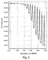
- Fig.2 shows the amplitude frequency response in mV on the Y axis (0 to 50mV), and frequency in the X axis (0 to 10GHz) of a channel comprising a pad connected using a Chip Scale Package (CSP) with the lowest available package parasitics (2nH, 0.6pF, negligible R), without any ESD structures, driving a 100mm long transmission line into the pad of another device packaged in the same manner.
- CSP Chip Scale Package
- FIG. 3 shows the same channel but with the reflected components removed from the driver end by eliminating the driver package parasitics, and with three curves representing different ESD structures on the driver, from no ESD to a B Class (Human Body Model) structure.
- both pads are perfectly terminated inside the chip to the line using an ideal resistor.
- Predefined equalisation that is using predetermined filter coefficients, make inherent assumptions about the line lengths, thickness, the dielectric parameters and other information which varies from application to application. Another weakness of the prior art is that the equalisation is applied at the transmitter, which assumes a single transmitter and single receiver architecture: this is impractical for real electronic systems which require multiple receivers as a minimum.
- noise An alternative or complementary aspect of this equalisation problem in a dynamic environment is noise. This has both pink component, where the amplitude per octave reduces with increasing frequency, and a component which is self induced or comes from electrical noise elsewhere in the system or the environment.
- the present invention can be applied to reduce this noise, by moving the signal out of regions of the spectrum where there is a deleterious noise component.
- Equalisation at the driver end of a channel has the obvious benefits of improving the signal to noise ratio at the receiver end.
- additional equalisation at each receiver is the best solution, but the problem then becomes one of how to determine how much equalisation to place where in the system.
- Solving this problem requires the ability to measure the parameters of the system, in effect a calibration of the channel, then loading appropriate values into integrated filter components such as variable resistors (MOSFETs) and variable capacitors (varicap diodes).
- MOSFETs variable resistors
- variable capacitors variable capacitors
- Another role of equalisation is to adapt the response of the channel to maximise the transfer function for the desired signal and to minimise the transmission response for noise.
- Digital signaling systems adopt a voltage or current level to be a logical state, and establish the gap between each of the states such that noise does not corrupt the digital value.
- a logical 0 may be specified as a voltage less than 0.8V and a logical 1 as a voltage above 1.6V: in this case the noise margin is 0.8V.
- An adaptive equaliser described in US 3,824,501 comprises an active filter having adjustable gain factor, a detection means for generating a control signal responsive to the peak signal level of the output signal, a means for adjusting said gain factor based on control signal.
- a decision region i.e. the "eye opening" of the eye diagram shown in Fig.1 is defined as the difference between the maximum peak and the minimum peak.
- Jitter is determined for the filtered signal, and the frequency response of the transfer function is varied accordingly by applying a digital adjustment signal to the transfer function structure.
- an adaptive equalizer according to US 5,991,339 has a digital feedback control using jitter as the adjustment criteria.
- the first object of the present invention is to provide an adaptive equalisation system that would overcome the deficiencies of the prior art and make corrections for deviations from ideal behaviour in a transmission medium or channel, such as caused by package parasitics, line discontinuities, skin effects, and non-linear dielectric constants, such that a higher data rate can be communicated across the medium with less amount of time and computation but still greater accuracy and reliability.
- the present invention is adaptive in that it measures artifacts of a signal transmitted through the medium by taking a series of samples, averaging the noise for each set of samples based on minimal BER (Bit Error Rate) approach, creating a full digital representation of the received signal and then adapting one or more filters to minimise the magnitude of those artifacts.
- minimal BER Bit Error Rate
- the above mentioned technique of estimating BER is described in the US application No. 10/038,868 entitled “Receiver With Automatic Skew Compensation” filed by the same applicants. According to this technique, the width of the eye diagram is measured directly, while there is no need in using clock and data recovery unit, metastable states are avoided, while transmitted data are latched at the moment when signal has the maximal stability.
- the benefit of this aspect of the current invention is to allow an increase in the maximum data rate.
- a second object of the present invention is to reduce the noise component from the signal such that the size of the voltage or current swing in transmitting a 1 or a 0 can be reduced, and that the noise generated by the system is also reduced.
- an adaptive equaliser for a communication channel comprising at least one driver for transmitting a signal along the channel and at least one receiver, the adaptive equaliser comprising:
- the adaptive equaliser uses the scanning means for scanning the signal at a variable voltage or current threshold to construct a digitised representation of the received signal, so that the filter parameters are adjusted based on this digital representation, however, other means for measuring the eye diagram are applicable as well.
- the adaptive equaliser automatically varies its characteristics as a function of the communication channel characteristics.
- An input signal carried by a transmission medium is provided to a variable filter whose characteristics are varied under feedback control.
- An output signal of the variable filter is input to a sampler.
- the specific feature of the sampler is that the signal is scanned at different voltage or current levels so as to construct a complete digital representation of the received signal. From the received signal, the distortion that the channel applies to the transmitted data is calculated.
- the present invention measures the filter response of the communication channel, or artifacts related thereto by sampling a calibration waveform generated by the transmitter. It applies this information to establish the correct coefficients in an equalisation filter that compensates for the distortion of the channel.
- the equaliser produces an output signal that is optimized for any transmission medium within a required communication pass band.
- the equalisation is applied first to the transmitter using the average signal distortion from a receiver, or all of the receivers, and then each receiver's equalisation is set up to tailor the equalisation to maximise the channel capacity for that receiver.
- the present invention can include in the same or a connected equalisation filter, a high pass filter to a signal with means to ensure the signal exceeds the cut-off frequency, such as by encoding the data and its strobe.
- a communication channel comprising two devices, a transmitting device A and a receiving device B, connected via transmission lines, such as a set of traces on a printed circuit board.
- transmission lines such as a set of traces on a printed circuit board.
- just one bit of the communication channel is shown as transmission line 21 for the reasons of clarity, but normally, a plurality of bits are used to connect devices using a parallel bus structure.
- Device A comprises an input data stream 2, which can be routed via multiplexer 3 to a driving register, such as flip-flop 5, then through a filter 9 to a buffer 11 which drives the transmission line 21.
- the transmission channel as shown by reference number 20 and outlined by a dotted line comprises driver impedance 13 and 15, package parasitics 17 and 19, the transmission line 21 itself, into the receiver which also has package parasitics 25, 27 and 29.
- the signal is buffered and amplified on the receiving device B, by a buffer 31, then filtered by a filter 35, and the signal is sampled in a sampler 39 which implements the means for measuring the signal.
- the digital sampler 39 is a comparator with a flip flop, such as a flip flop with a differential input, where the incoming signal is compared to a reference level generated by a reference DAC (digital-to-analog converter) 37.
- a finite state machine 33 estimates the width of the eye opening based on information received from the sampler 39.
- the filter parameters, operation of the DAC and the protocol is controlled in the receiver by a control means, such as the same finite state machine 33 which may be implemented most easily using a micro-controller with associated ROM and RAM memory.
- the transmitting device A also has a state machine 7, which may be a micro-controller, which drives a pattern generator 1 to establish a data pattern during a calibration or setup phase for the channel, and this pattern can be switched into the channel during the calibration phase by means of the multiplexer 3.
- the entire system operates using a clock generator 23 which may be located anywhere in the system.
- Data on the captured signals are communicated back to the transmitting device A on return channel 43, which may be the same channel as used to transmit the original pattern running in the opposite direction, or a separate low speed link.
- the link can operate at a much slower speed than the link would normally operate after the equalisation processes described herein have been completed.
- the first step determines the characteristic of the transmission channel 20. To do this, a regular data pattern is generated by the pattern generator 1 and this is routed into the channel via the multiplexor 3 instead of the data stream, which is normally absent during this reset or startup phase of the system.
- the pattern is sampled by the receiver B to generate a representation of the received signal. To do this, the receiver takes a series of samples, average out the noise for each set of samples.
- the integrity of the received data can be observed using an eye diagram, such as in Fig. 7.
- the eye in the very centre is the region where the data is stable and is strobed.
- the eye diagram shows time in the X domain, in picoseconds in Fig. 7, and voltage or current in the Y domain, in mV in Fig.7.
- To receive data securely it is necessary to sample the data (that is, close a gate in the time domain), with the switching threshold of the gate as close as possible to the centre of the eye.
- a technique for tracking the centre of the eye in the voltage or current domain is described in US patent application US 2003014683 A, published on January 16, 2003.
- the reference voltage may be swept during the sampling process. This process of sending a signal and then sampling the signal to create a representation of the signal is a common and widely known process used in oscilloscopes and other measurement equipment.
- the distortion that the channel applies to the transmitted data is determined, and from this distortion, equalisation parameters are determined for the filters.
- the distortion that the channel applies to the signal is determined as a difference between the signal at the receiver and the signal that is transmitted into the channel.
- the means for measuring the received signal takes a series of successive samples of the received signal, determines the width of the eye opening, selects the sampling point as a point where the Bit Error Rate is minimal and estimates the distortion with reference to this sample as described in detail in US application US 2003014683 by the same applicant.
- the Bit Error Rate is calculated as a probability to sample wrong symbol in a series of symbols.
- correction for the distortion in the channel can be a simple matter of determining the time constant for a fast signal.
- Fig. 4 shows the received signal from a perfect step sent from the transmitter through a transmission medium including the ESD structures, package parasitic and a short line ideally terminated.
- the filter response of the transmission medium can be calculated as: based on Laplace function and Hilbert transformation, respectively, as shall be evident for a specialist in the art.
- a filter to correct this response can be implemented as a simple conventional RC filter as shown in Fig. 8a, or using the components and circuit shown in Fig. 8b, comprising a first order filter using elements easily fabricated in silicon.
- the characteristics of the components, such as R, C, can be determined by the same process as used to determine the frequency response of the system, to compensate for process variances.
- a preferred process to establish the filter parameters is to iteratively load values, including R and C values, measure the response, such as voltage or current amplitude of the signal in the channel and tune the values as a function of the response.
- the procedure is to follow the gradient of the transfer function to find the optimal values, but in complex cases, a monte-carlo approach is necessary to find the optimal equalisation.
- the monte-carlo process can start with a seed value determined in during the design process, from initial device characterisation, or from saving the values of the previous calibration in the system.
- the amount of time needed to perform the calibration can be significant, therefore the expediency of saving the last values used, then loading these values as the initial state the next time the system is powered up, is evident and can greatly extend the utility of the present invention.
- the values can be stored in any form of non-volatile memory or memory with battery backup.
- the monte-carlo approach resolves filter characteristics in realistic systems where the signal includes reflections. That is, in addition to frequency dependent effects such as Skin Effect Attenuation, the signal is modulated by reflections from nodes within the channel that are a function of the data previously sent down the channel and by parasitics in the driver and receiver packaging. It is impossible for a symbol received at a receiver to be affected by subsequent bits sent through the channel assuming the same rise time is used for all symbols transmitted, so only the static distortion of the channel and its historic content need be considered.
- the transmitter on power up or at other times appropriate to the application, sends a regular signal at an intermediate frequency used within the channel.
- a system with a 1MHz to 10GHz channel bandwidth operating with a copper transmission line 1m long may send a 10MHz repetitive signal for this purpose.
- the receiver will lock onto this signal, and then take successive samples, moving the sample threshold voltage or current between groups of samples, to construct a digitised representation of the received signal.
- the receiver can then statically compute the filter required to convolve this signal to reconstruct the original repetitive signal.
- the constants for the filter to implement this inverse filtering operation can then be applied to a filter, with as many taps as necessary.
- the number of taps depends on the nature of the channel. For example, a simple point to point system with good termination may require only 3 taps in a transition filter to correct for skin effects but parasitics require many more taps.
- a channel with multiple reflective nodes and poor termination across branches of the channel can require 9 more taps.
- Another advantage of the present invention is that it minimises the computation required.
- Approaches such as measuring the actual amplitude - frequency response and phase-frequency response using swept signals, such as described by Chadwick in US patent 5,557,640 for application in RF systems, are entirely impractical in most digital systems due to their inability to generate sinusoidal signals and the difficulty in determining filter parameters directly from such data given the non-ideal nature of the filter components and process variations.
- the present invention avoids all need to calculate filter parameters from frequency domain data.
- the approach described herein uses a digital signal, which will have limitations in its rise and fall slew rates as well as other variations from the ideal, to tune the actual filter components to optimise the response, namely to improve the data bandwidth of the channel or intersymbol skew, or increasing the area in the eye diagram, or reducing settling time.
- Fig.1 shows a driver, with the ability to apply a repetitive pulse train with each pulse of duration greater than the total settling time of the transmission medium, the ability to measure voltage using a time gate on a comparator to build up a representation of the signal as amplitude in time.
- the transmission channel characteristic is derived from this pulse train, treating the pulse as an integral of a Dirac impulse to a system convolved with the driver characteristic.
- the characterisation preferably includes the driver and other integrated semiconductor components, such as the preamplifier, ESD structure and receiver, as part of the overall channel response.
- Each of the receivers applies a similar equalisation process while the driver is still generating the pulse train, but after a delay while the driver is performing its equalisation.
- the duration of the pulse train is determined as a trade off of time against the quality of the equalisation: a long train allows more samples to be taken.
- the accuracy of measurement of a particular point is proportional to the square root of the number of samples.
- the resolution of the comparator should not be less than the noise in the channel: if it is, then it is necessary to add artificial noise during the calibration process to allow points between the quantisation steps of the comparator to be resolved.
- the resolution of the comparator should preferably be matched to the resolution in the time domain of the sampling system over the period of the rise time. In this example, if the rise time is 40ps then with 5ps steps, the time data comprises 8 points over the rise time of the signal. For 8 voltage points, plus noise, suggests 16 voltage points need to be measured, to give a 4 bit result.
- the total time required for this channel is thus 16 times 12.5x10 ⁇ 6, plus the settling time for moving the voltage steps 16 times unless a sloping reference algorithm is used. This gives a total driver calibration time for a 1m 10GHz channel of 20 seconds.
- This calibration time can be reduced very substantially by various methods:
- each part of the filter is separated such as by an amplifier, it is possible to calibrate each of the filter elements: when the filter elements are interconnected such as in a filter with 9 poles and zeros.
- Adding voltage noise during calibration can reduce the total calibration time by allowing the number of passes to be reduced because the values can be averaged with a known noise characteristic.
- the received signal will include noise from adjacent channels, from power supplies, EMI, thermal noise and other sources.
- the noise voltage will tend to be asynchronous with the sampling process but give a window, which may be large, that effectively reduces the available transmission channel bandwidth as seen in an eye diagram such as in Fig. 7.
- the signal in this modified implementation is modified to ensure it exceeds the cut off frequency of the filter, and the filter has a high pass response.
- Methods for doing this include Manchester encoding of the signal, or inverting both data and clock or data and a strobe signal, for example, if any signal in the 8 bit wide interface has more than 16 cycles in the same state, in this example, the clock and all the data would invert.
- the inversion can be detected by the receiver in that the clock received is entirely out of phase with the PLL.
- a distinct line carrying a complement of the clock can be used to signal data inversion: for example the clock would run continuously as a differential pair, but when the clock has a data inversion, then one of the pair is inverted.
- a suitable receiver can then both receive the clock with the data and determine when to apply an inverse coding, in this case just by inverting the data.
- the filter introduces a frequency dependent phase shift, or skew, on the incoming signal.
- the cut-off frequency is chosen such that the skew is within predetermined limits across the pass band of the filter.
- Alternative solutions such as a pattern dependent delay can be implemented by comparing for each data line the current data and n previous states with a register holding values that are applied to a vernier delay to create an inverse skew, such that the data is deskewed by the filter on arriving at the receiver, such as in US Patent Application US 2002051506-A, pulished on May 02, 2002.
- the amount of receiver hysteresis required in a system with background EMI can be determined by a calibration process, or a process of continuous feedback.
- the bit error rate (BER) of the link is measured for different levels of hysteresis, and the optimal level chosen: this is normally zero, but it is expedient in many circumstances to operate with a constant BER and adjust the hysteresis accordingly.
- the level of hysteresis After the level of hysteresis has been determined, it is necessary to vary either the slew rate such as by changing the current used to drive the system, or change the data rate.
- the system seeks to minimise both the hysteresis and the slew rate for minimising interference with other system parameters.
- a system with non-zero BER will normally require an error encoding and decoding system to detect for the presence of and remove noise artifacts within the signal.
- Synchronous noise from other system components is preferably minimised by choosing parts with the slowest slew rates. Obviously, locating a block of logic using a logic family with a 100ps rise and fall time, will create substantial interference with a low swing system such as that described herein. Choice of a logic family with, for example, a 3ns slew rate to drive peripherals with the primary logic running at 100Gbps with the cut-off filter at even 10GHz, will minimise the amount of interference.
- Information gathered by the receiver during the calibration phase of the channel can be communicated to the driver using either a separate low speed channel, or by using the primary channel working at a lower frequency, such as 133MHz.
- Channels with multiple drivers and multiple receivers can be calibrated by each of the drivers performing a calibration. This requires a number of calibration passes equal to the number of drivers, or an average driver response being determined from a sample of the drivers and this average channel response being equalised by all the drivers.
- An equalisation process involves applying an approximation to the inverse of the channel response over the pass bandwidth.
- the filter components implement this inverse function, such that the data is applied to the filter, which amplifies, or at high frequencies more typically attenuates, the data signal such that the combination of the equalisation filter and the channel response is as flat as possible, except for in the case of the extended implementation of the present invention, low frequencies or frequencies in a noise spectrum are further attenuated.
Claims (17)
- Égaliseur adaptatif (7, 9, 11, 31, 35, 33) comprenant un filtre variable (9, 35) pour modifier le signal, un moyen (39) pour mesurer le signal reçu et un moyen de commande (7, 33) pour ajuster les paramètres de filtre (9, 35) ; dans lequel :caractérisé en ce que la largeur de l'ouverture en oeil dans le diagramme en oeil du signal reçu est mesurée en utilisant un moyen de balayage (37, 39) pour comparer le signal avec un seuil de tension ou de courant variable.le moyen (39) pour mesurer le signal reçu détermine la largeur de l'ouverture en oeil dans le diagramme en oeil du signal reçu ; et les paramètres de filtre (9, 35) sont ajustés par le moyen de commande (7, 33) sur la base de la largeur déterminée du diagramme en oeil,
- Égaliseur adaptatif selon la revendication 1, dans lequel le moyen de commande (7, 33) construit une représentation numérisée du signal reçu, les paramètres de filtre (9, 35) étant ajustés sur la base de la représentation numérisée construite.
- Égaliseur adaptatif selon la revendication 1 ou 2, dans lequel le moyen de commande (7, 33) charge itérativement des valeurs de paramètres de filtres (9, 35) et accorde les valeurs en fonction du signal reçu pour enrouler le signal pour reconstruire le signal d'entrée.
- Égaliseur adaptatif selon la revendication 3, dans lequel le moyen de commande (7, 33) réalise une itération en utilisant une approche Monté Carlo pour trouver une égalisation optimale.
- Égaliseur adaptatif selon la revendication 3, dans lequel le moyen de commande (7, 33) réalise une itération en suivant le gradient de la fonction de transfert du filtre.
- Égaliseur adaptatif selon l'une quelconque des revendications 1 à 4, dans lequel le moyen (39) pour mesurer le signal reçu prend une série d'échantillons successifs du signal reçu et sélectionne le point d'échantillon avec un taux d'erreur binaire minimal pour construire une représentation numérisée du signal reçu.
- Égaliseur adaptatif selon l'une quelconque des revendications 1 à 6, dans lequel un bruit d'amplitude ou un autre signal est appliqué au moyen (39) pour mesurer le signal pour améliorer la résolution des mesures.
- Égaliseur adaptatif selon l'une quelconque des revendications 1 à 7, dans lequel les composantes de filtre (9, 35) sont pré-calibrées.
- Canal de communication comprenant au moins un dispositif de commande (11) pour transmettre un signal d'entrée le long du canal (21), au moins un récepteur (31) et un égaliseur adaptatif comprenant un filtre variable (9, 35) pour modifier le signal, un moyen (39) pour mesurer le signal reçu et un moyen de commande (7, 33) pour ajuster les paramètres de filtre (9, 35), caractérisé en ce que l'égaliseur est comme exposé dans l'une quelconque des revendications 1 à 8.
- Canal selon la revendication 9, dans lequel les composantes de filtre (9, 35) sont intégrées à la fois dans l'émetteur (11) et le récepteur (31).
- Canal selon l'une quelconque des revendications 9 et 10 dans lequel la puce sur laquelle le récepteur (31) est situé communique des mesures à la puce sur laquelle le dispositif de commande est situé.
- Canal de communication selon l'une quelconque des revendications 1 à 11, comprenant une pluralité de récepteurs (31), chaque récepteur comprenant l'égaliseur adaptatif, dans lequel le filtre (9) sur l'émetteur (11) est réglé pour compenser la distorsion de signal moyen sur les récepteurs et les filtres (35) dans les récepteurs sont réglés pour compenser la différence entre le signal moyen sur les récepteurs et le signal particulier sur chaque récepteur.
- Canal de communication selon l'une quelconque des revendications 9 à 12 comprenant en outre une source de signal, préférablement du bruit, qui est appliquée au récepteur (31) afin que la résolution d'un comparateur réalisant des mesures de tension soit améliorée.
- Canal selon la revendication 13, dans lequel les récepteurs ou comparateurs sont décalés en temps ou en tension de référence.
- Procédé d'émission de données le long d'un canal de communication comprenant au moins un dispositif de commande (11) pour émettre un signal le long du canal (21), au moins un récepteur et un égaliseur adaptatif, caractérisé en ce que le canal communication est comme exposé dans l'une quelconque des revendications 6 à 14.
- Procédé pour l'égalisation des caractéristiques d'un canal de communication (20), dans lequel l'égalisation est réalisée en appliquant au canal un traitement de calibrage comprenant les étapes de :caractérisé en ce que la largeur de l'ouverture en oeil dans le diagramme en oeil du signal filtré reçu est mesurée en comparant le signal avec un seuil de tension ou de courant variable.commande d'un signal dans le canal (20) ;application d'une fonction de transfert d'un filtre (9, 35) au signal reçu pour produire un signal filtré ;mesure de la largeur de l'ouverture en oeil dans le diagramme en oeil du signal filtré reçu ;ajustement des paramètres de la fonction de transfert dans le filtre (9, 35) pour modifier le signal sur la base de la largeur déterminée de l'ouverture en oeil,
- Procédé selon la revendication 16, dans lequel le procédé est réalisé en utilisant un égaliseur adaptatif selon l'une quelconque des revendications 1 à 8 ou un canal de communication selon l'une quelconque des revendications 9 à 14.
Applications Claiming Priority (3)
| Application Number | Priority Date | Filing Date | Title |
|---|---|---|---|
| US31590701P | 2001-08-28 | 2001-08-28 | |
| US315907P | 2001-08-28 | ||
| PCT/IB2002/003542 WO2003019810A2 (fr) | 2001-08-28 | 2002-08-28 | Egalisateur adaptatif permettant de reduire la distorsion dans un canal de communication |
Publications (2)
| Publication Number | Publication Date |
|---|---|
| EP1423923A2 EP1423923A2 (fr) | 2004-06-02 |
| EP1423923B1 true EP1423923B1 (fr) | 2005-05-11 |
Family
ID=23226581
Family Applications (1)
| Application Number | Title | Priority Date | Filing Date |
|---|---|---|---|
| EP02758748A Expired - Fee Related EP1423923B1 (fr) | 2001-08-28 | 2002-08-28 | Egalisateur adaptatif permettant de reduire la distorsion dans un canal de communication |
Country Status (5)
| Country | Link |
|---|---|
| US (1) | US20030043900A1 (fr) |
| EP (1) | EP1423923B1 (fr) |
| AU (1) | AU2002324305A1 (fr) |
| DE (1) | DE60204156T2 (fr) |
| WO (1) | WO2003019810A2 (fr) |
Cited By (1)
| Publication number | Priority date | Publication date | Assignee | Title |
|---|---|---|---|---|
| US9008196B2 (en) | 2011-04-28 | 2015-04-14 | International Business Machines Corporation | Updating interface settings for an interface |
Families Citing this family (11)
| Publication number | Priority date | Publication date | Assignee | Title |
|---|---|---|---|---|
| US7116851B2 (en) * | 2001-10-09 | 2006-10-03 | Infinera Corporation | Optical signal receiver, an associated photonic integrated circuit (RxPIC), and method improving performance |
| JP4259042B2 (ja) * | 2002-06-10 | 2009-04-30 | 日本電気株式会社 | 等化装置及び等化方法並びに伝送装置 |
| US7352815B2 (en) * | 2003-06-23 | 2008-04-01 | International Business Machines Corporation | Data transceiver and method for equalizing the data eye of a differential input data signal |
| US20050071112A1 (en) * | 2003-09-29 | 2005-03-31 | Intel Corporation | Method and apparatus for channel-based testing |
| US8750725B2 (en) * | 2003-11-18 | 2014-06-10 | Finisar Corporation | Digital optical receiving module, and a method for monitoring the signal quality of a transmitted, modulated optical signal |
| US7424382B2 (en) * | 2004-11-23 | 2008-09-09 | Agilent Technologies, Inc. | Characterizing eye diagrams |
| CN1996273A (zh) * | 2006-01-04 | 2007-07-11 | 鸿富锦精密工业(深圳)有限公司 | 高速信号传输电路 |
| WO2009003129A2 (fr) * | 2007-06-27 | 2008-12-31 | Rambus Inc. | Procédés et circuits pour une égalisation adaptative et une caractérisation de canal en utilisant des données en direct |
| WO2013137911A1 (fr) * | 2012-03-16 | 2013-09-19 | Song Sanquan | Appareil et système pour égalisation à commutation |
| US9673773B2 (en) | 2015-06-23 | 2017-06-06 | Qualcomm Incorporated | Signal interconnect with high pass filter |
| CN114938366A (zh) * | 2022-05-10 | 2022-08-23 | 邦彦技术股份有限公司 | 一种基于bios可配置眼图参数的方法及系统 |
Family Cites Families (7)
| Publication number | Priority date | Publication date | Assignee | Title |
|---|---|---|---|---|
| US3824501A (en) * | 1973-07-12 | 1974-07-16 | Bell Telephone Labor Inc | Automatic cable equalizer |
| US4759035A (en) * | 1987-10-01 | 1988-07-19 | Adtran | Digitally controlled, all rate equalizer |
| US5293405A (en) * | 1991-10-31 | 1994-03-08 | International Business Machines Corp. | Adaptive equalization and regeneration system |
| US5751766A (en) * | 1995-04-27 | 1998-05-12 | Applied Signal Technology, Inc. | Non-invasive digital communications test system |
| US5991339A (en) * | 1998-01-16 | 1999-11-23 | Intel Corporation | Adaptive equalization using a minimum- jitter criterion |
| US6570406B2 (en) * | 2000-11-13 | 2003-05-27 | Primarion, Inc. | Method and circuit for pre-emphasis equalization in high speed data communications |
| JP3798640B2 (ja) * | 2001-03-02 | 2006-07-19 | 富士通株式会社 | 受信装置及び受信信号の波形劣化補償方法並びに波形劣化検出装置及び方法並びに波形測定装置及び方法 |
-
2002
- 2002-08-28 WO PCT/IB2002/003542 patent/WO2003019810A2/fr not_active Application Discontinuation
- 2002-08-28 DE DE60204156T patent/DE60204156T2/de not_active Expired - Fee Related
- 2002-08-28 AU AU2002324305A patent/AU2002324305A1/en not_active Abandoned
- 2002-08-28 EP EP02758748A patent/EP1423923B1/fr not_active Expired - Fee Related
- 2002-08-28 US US10/229,082 patent/US20030043900A1/en not_active Abandoned
Cited By (1)
| Publication number | Priority date | Publication date | Assignee | Title |
|---|---|---|---|---|
| US9008196B2 (en) | 2011-04-28 | 2015-04-14 | International Business Machines Corporation | Updating interface settings for an interface |
Also Published As
| Publication number | Publication date |
|---|---|
| DE60204156T2 (de) | 2006-02-09 |
| US20030043900A1 (en) | 2003-03-06 |
| DE60204156D1 (de) | 2005-06-16 |
| EP1423923A2 (fr) | 2004-06-02 |
| WO2003019810A3 (fr) | 2003-10-02 |
| WO2003019810A2 (fr) | 2003-03-06 |
| AU2002324305A1 (en) | 2003-03-10 |
Similar Documents
| Publication | Publication Date | Title |
|---|---|---|
| Horowitz et al. | High-speed electrical signaling: Overview and limitations | |
| US11563554B2 (en) | Method for measuring and correcting multi-wire skew | |
| US10284395B2 (en) | Time-based decision feedback equalization | |
| EP1423923B1 (fr) | Egalisateur adaptatif permettant de reduire la distorsion dans un canal de communication | |
| US7278069B2 (en) | Data transmission apparatus for high-speed transmission of digital data and method for automatic skew calibration | |
| US7321259B1 (en) | Programmable logic enabled dynamic offset cancellation | |
| EP3743785B1 (fr) | Procédé et système d'étalonnage de désalignement de fils multiples | |
| US20090296851A1 (en) | Pre-emphasis circuit | |
| US8581619B2 (en) | Impedance calibration circuit and method | |
| US20090174448A1 (en) | Differential communication link with skew compensation circuit | |
| KR100593784B1 (ko) | 위상 제어를 샘플링하기 위한 방법 | |
| US7957412B2 (en) | Lonely pulse compensation | |
| US6188721B1 (en) | System and method for adaptive equalization of a waveform independent of absolute waveform peak value | |
| US20020097805A1 (en) | Replica driver mismatch correction using a variable offset comparator | |
| Gerfers et al. | A 0.2–2 Gb/s 6x OSR receiver using a digitally self-adaptive equalizer | |
| WO2002039629A9 (fr) | Systeme de calibrage de temps de voie | |
| Fan et al. | A 32 Gb/s Simultaneous Bidirectional Source-Synchronous Transceiver with Adaptive Echo Cancellation in 28nm CMOS | |
| US9484916B1 (en) | Adaptive on-chip termination circuitry | |
| US8798568B2 (en) | Signal transmission method, transmission circuit and apparatus | |
| WO2017213138A1 (fr) | Dispositif de réception | |
| US11095487B1 (en) | Operating a wireline receiver with a tunable timing characteristic | |
| EP3954046B1 (fr) | Ajustement dynamique du temps d'intégration d'un échantillonneur de données horloge utilisant un circuit d'étalonnage analogique statique | |
| JP3815437B2 (ja) | インターフェース回路 | |
| CN110383782B (zh) | 信号传输装置 | |
| US20110150136A1 (en) | Duty cycle compensating digital data receiver |
Legal Events
| Date | Code | Title | Description |
|---|---|---|---|
| PUAI | Public reference made under article 153(3) epc to a published international application that has entered the european phase |
Free format text: ORIGINAL CODE: 0009012 |
|
| 17P | Request for examination filed |
Effective date: 20040326 |
|
| AK | Designated contracting states |
Kind code of ref document: A2 Designated state(s): AT BE BG CH CY CZ DE DK EE ES FI FR GB GR IE IT LI LU MC NL PT SE SK TR |
|
| AX | Request for extension of the european patent |
Extension state: AL LT LV MK RO SI |
|
| 17Q | First examination report despatched |
Effective date: 20040603 |
|
| GRAP | Despatch of communication of intention to grant a patent |
Free format text: ORIGINAL CODE: EPIDOSNIGR1 |
|
| GRAS | Grant fee paid |
Free format text: ORIGINAL CODE: EPIDOSNIGR3 |
|
| GRAA | (expected) grant |
Free format text: ORIGINAL CODE: 0009210 |
|
| RAP1 | Party data changed (applicant data changed or rights of an application transferred) |
Owner name: ACUID CORPORATION (GUERNSEY) LIMITED |
|
| AK | Designated contracting states |
Kind code of ref document: B1 Designated state(s): DE GB |
|
| RBV | Designated contracting states (corrected) |
Designated state(s): DE GB |
|
| REG | Reference to a national code |
Ref country code: GB Ref legal event code: FG4D |
|
| REG | Reference to a national code |
Ref country code: IE Ref legal event code: FG4D |
|
| REF | Corresponds to: |
Ref document number: 60204156 Country of ref document: DE Date of ref document: 20050616 Kind code of ref document: P |
|
| PG25 | Lapsed in a contracting state [announced via postgrant information from national office to epo] |
Ref country code: DE Free format text: LAPSE BECAUSE OF NON-PAYMENT OF DUE FEES Effective date: 20060301 |
|
| PLBE | No opposition filed within time limit |
Free format text: ORIGINAL CODE: 0009261 |
|
| STAA | Information on the status of an ep patent application or granted ep patent |
Free format text: STATUS: NO OPPOSITION FILED WITHIN TIME LIMIT |
|
| 26N | No opposition filed |
Effective date: 20060214 |
|
| GBPC | Gb: european patent ceased through non-payment of renewal fee |
Effective date: 20060828 |
|
| PG25 | Lapsed in a contracting state [announced via postgrant information from national office to epo] |
Ref country code: GB Free format text: LAPSE BECAUSE OF NON-PAYMENT OF DUE FEES Effective date: 20060828 |