EP1423751B1 - Dispositif de maniement de signal optique integre - Google Patents
Dispositif de maniement de signal optique integre Download PDFInfo
- Publication number
- EP1423751B1 EP1423751B1 EP02735621A EP02735621A EP1423751B1 EP 1423751 B1 EP1423751 B1 EP 1423751B1 EP 02735621 A EP02735621 A EP 02735621A EP 02735621 A EP02735621 A EP 02735621A EP 1423751 B1 EP1423751 B1 EP 1423751B1
- Authority
- EP
- European Patent Office
- Prior art keywords
- resonator
- waveguide
- region
- arrangement
- light
- Prior art date
- Legal status (The legal status is an assumption and is not a legal conclusion. Google has not performed a legal analysis and makes no representation as to the accuracy of the status listed.)
- Expired - Lifetime
Links
Images


Classifications
-
- G—PHYSICS
- G02—OPTICS
- G02F—OPTICAL DEVICES OR ARRANGEMENTS FOR THE CONTROL OF LIGHT BY MODIFICATION OF THE OPTICAL PROPERTIES OF THE MEDIA OF THE ELEMENTS INVOLVED THEREIN; NON-LINEAR OPTICS; FREQUENCY-CHANGING OF LIGHT; OPTICAL LOGIC ELEMENTS; OPTICAL ANALOGUE/DIGITAL CONVERTERS
- G02F1/00—Devices or arrangements for the control of the intensity, colour, phase, polarisation or direction of light arriving from an independent light source, e.g. switching, gating or modulating; Non-linear optics
- G02F1/29—Devices or arrangements for the control of the intensity, colour, phase, polarisation or direction of light arriving from an independent light source, e.g. switching, gating or modulating; Non-linear optics for the control of the position or the direction of light beams, i.e. deflection
- G02F1/31—Digital deflection, i.e. optical switching
- G02F1/313—Digital deflection, i.e. optical switching in an optical waveguide structure
- G02F1/3132—Digital deflection, i.e. optical switching in an optical waveguide structure of directional coupler type
-
- G—PHYSICS
- G02—OPTICS
- G02F—OPTICAL DEVICES OR ARRANGEMENTS FOR THE CONTROL OF LIGHT BY MODIFICATION OF THE OPTICAL PROPERTIES OF THE MEDIA OF THE ELEMENTS INVOLVED THEREIN; NON-LINEAR OPTICS; FREQUENCY-CHANGING OF LIGHT; OPTICAL LOGIC ELEMENTS; OPTICAL ANALOGUE/DIGITAL CONVERTERS
- G02F1/00—Devices or arrangements for the control of the intensity, colour, phase, polarisation or direction of light arriving from an independent light source, e.g. switching, gating or modulating; Non-linear optics
- G02F1/01—Devices or arrangements for the control of the intensity, colour, phase, polarisation or direction of light arriving from an independent light source, e.g. switching, gating or modulating; Non-linear optics for the control of the intensity, phase, polarisation or colour
- G02F1/0147—Devices or arrangements for the control of the intensity, colour, phase, polarisation or direction of light arriving from an independent light source, e.g. switching, gating or modulating; Non-linear optics for the control of the intensity, phase, polarisation or colour based on thermo-optic effects
-
- G—PHYSICS
- G02—OPTICS
- G02F—OPTICAL DEVICES OR ARRANGEMENTS FOR THE CONTROL OF LIGHT BY MODIFICATION OF THE OPTICAL PROPERTIES OF THE MEDIA OF THE ELEMENTS INVOLVED THEREIN; NON-LINEAR OPTICS; FREQUENCY-CHANGING OF LIGHT; OPTICAL LOGIC ELEMENTS; OPTICAL ANALOGUE/DIGITAL CONVERTERS
- G02F2203/00—Function characteristic
- G02F2203/15—Function characteristic involving resonance effects, e.g. resonantly enhanced interaction
Definitions
- This invention relates to integrated optical signal handling devices, for example (though not exclusively) devices for optical signal routing, switching, multiplexing or demultiplexing.
- DWDM dense wavelength division multiplexing
- DWDM employs many closely spaced optical carrier wavelengths, multiplexed together onto a single waveguide such as an optical fibre.
- the carrier wavelengths are spaced apart by as little as 50 GHz in a spacing arrangement defined by an ITU (International Telecommunications Union) channel "grid".
- ITU International Telecommunications Union
- Each carrier wavelength may be modulated to provide a respective data transmission channel.
- the data rate of each channel can be kept down to a manageable level, so avoiding the need for expensive very high data rate optical transmitters, optical receivers and associated electronics.
- DWDM can make better use of the inherent bandwidth of an optical fibre link, including links which have already been installed. It also allows a link to be upgraded gradually, simply by adding new channels.
- DWDM DWDM-optical handling of telecommunications signals, rather than via an intermediate conversion to and from the electrical domain.
- optical components such as routers, switches, cross-point networks, channel add-drop multiplexers, variable optical attenuators and so on. It has been proposed that so-called optical integrated circuits offer potential to meet these needs.
- One previously proposed arrangement is to demultiplex an input WDM optical signal into individual wavelength channels using, for example, one or more arrayed waveguide devices (AWGs).
- the N individual wavelength channels can then be switched, routed or substituted, for example by an N x N optical crosspoint switch, before being multiplexed back into an output WDM signal by a corresponding group of one or more AWGs.
- this arrangement would fulfil the required functionality, it is perceived to be very complex (particularly a large N x N crosspoint switch) and can introduce unwanted losses because of the number of components forming the optical signal path through the apparatus.
- silicon and/or silica based materials it would be physically very large in comparison to many other integrated optical devices. If, for example, it is desired only to have the facility to (selectively) tap off one wavelength channel from a WDM signal, the solution described above would be considered far too complex for this purpose.
- This invention provides an integrated optical signal handling device comprising:
- the invention builds on integrated resonator cavity arrangements such as the previously proposed "disk resonator” arrangement - or other arrangements such as generally circular, annular, elliptical and/or substantially planar resonator arrangements - to provide an integrated optical signal handling device having controllable signal handling properties.
- the invention provides a resonator with an associated heating and/or cooling arrangement which, by varying the temperature of at least the resonator region can alter the coupling wavelengths at which light is coupled between the resonator and a nearby waveguide.
- Several useful and controllable optical components can be formed using this basic arrangement.
- an input WDM signal can be directed along the waveguide.
- the resonator temperature is set so that at the wavelength of a WDM channel of interest light is coupled between the waveguide and the resonator. So, the channel of interest can be removed form the input signal (a channel "drop" function). That channel can be routed elsewhere in embodiments of the invention by passing another waveguide near to the resonator so that the channel of interest is coupled into that waveguide for output.
- a channel "add" function can be achieved in embodiments of the invention by launching a channel to be added, with the coupling wavelength set to that channel's wavelength, into the second waveguide; it is coupled into the resonator and out to the first waveguide.
- the resonator could be formed of a glass or similar core material, but to achieve a greater variation of the optical properties of the resonator with temperature, and also to facilitate the fabrication process, it is preferred that the resonator region is formed of a polymer material.
- the resonator region is a generally ring- or generally disk-shaped region. While a precise circular or elliptical shape can be useful for predictability of performance, for example, it is also noted that small deviations from such a mathematically correct shape can in fact give an advantageously higher "Q" factor (see below) in the resonator.
- any references to the shape of any fabricated formation are to be considered within the normal tolerance limits imposed by engineering aspects of the fabrication process itself, including those relevant to the shape of the resonator in the plane of or perpendicular to the substrate and also those relevant to the degree to which the sides of any planar shape can be made perpendicular to the substrate.
- the heating and/or cooling arrangement comprises at least an electrical heating element and/or at least a Peltier element.
- an optical heating arrangement such as one or more laser devices arranged to irradiate at least the resonator region could be used.
- This arrangement has the advantage of allowing the heating arrangement to be slightly more remote from the active optical components (e.g. the resonator) and avoiding the need for electrical conductors to be fabricated over the resonator. This in turn could lead to more efficient use of the substrate area, as the electrical connections are often a space-limiting factor in arrays of integrated optical components.
- Another advantage is the possibility of maintenance or modification of the heating arrangement without dismantling the resonator arrangement.
- the waveguide could be disposed at least partly alongside (i.e. in the plane of) the resonator, for efficient use of the substrate area and general ease of fabrication it is preferred that the waveguide is not disposed in the plane of the resonator region.
- the resonator region and the waveguide are formed so as to overly, at least in part, one another (here the skilled man will appreciate that the wording used does not necessarily imply an order of fabrication of the respective parts on the substrate).
- the resonator could be bounded by cladding material, but in order to reduce bending losses in the resonator (or, put another way, to allow a physically smaller resonator to be used) it is preferred that the resonator region is bounded, in the plane of the resonator region, by an air gap.
- a polymer cladding layer is disposed on the resonator region.
- an expansion in the planar direction of the resonator can change the dimensions of the resonator in such a manner as to counteract the change in refractive index brought on by a temperature change.
- the resonator is constrained (e.g. by a cladding) to reduce expansion / contraction in a planar substrate direction.
- the device comprises at least a second light-guiding waveguide formed in or on the substrate adjacent to the resonator region so as to allow optical coupling between the waveguide and the resonator region at one or more coupling wavelengths.
- Suzuki et al in the paper "Integrated-optic double-ring resonators with a wide free spectral range of 14GHz", Journal of Lightwave Technology, vol. 13, no. 8, pp 1766-1771, 1995 , propose a double ring resonator where light couples from a first waveguide into a first ring or disk, from which it couples to another adjacent ring or disk, finally coupling from the second ring or disk into an output waveguide.
- This idea has been further developed by Little et al in the paper “Microring resonator channel dropping filters”, Journal of Lightwave Technology, vol. 15, no. 6, pp 998-1005, 1997 .
- WO 01/38905 A2 discloses a ring resonator employing local thermal tuning. The heating is used to vary the resonator's resonance wavelength in order to tune the device.
- WO 01/33267 A1 discloses a tunable OADM including a ring resonator which is thermally tuned by a grating reflector.
- This invention also provides an integrated optical signal handling device comprising:
- This aspect of the invention builds on integrated resonator cavity arrangements such as the previously proposed "double-disk resonator” arrangement - or other arrangements such as generally circular, annular, elliptical and/or substantially plural planar resonator arrangements - to provide an integrated optical signal handling device having controllable signal handling properties.
- the invention provides a device having a multi-cavity (e.g. two cavity) resonator arrangement with an associated heating and/or cooling arrangement which, by varying the temperature of at least a resonator region of the resonator arrangement can alter the coupling wavelengths or other properties by which light is coupled between the resonator cavities.
- a multi-cavity e.g. two cavity
- Several useful and controllable optical components can be formed using this basic arrangement.
- the device comprises at least a second light-guiding waveguide formed in or on the substrate adjacent to the resonator region so as to allow optical coupling between the waveguide and the resonator region at one or more coupling wavelengths.
- the resonator arrangement comprises a series arrangement of two or more resonator cavities so that, in use, light may be coupled:
- the resonator arrangement may provide a parallel arrangement of two or more resonator cavities linking the light guiding waveguide and the second light guiding waveguide so that light may be coupled between the light guiding waveguide and the second light guiding waveguide via two or more resonator cavities at a time.
- the waveguide In order to couple light between a disk / ring-like resonator and a waveguide, the waveguide is generally either positioned substantially in the plane of the resonator but displaced laterally, or positioned out of the plane of the resonator and at least partially overlapping in the lateral direction. This latter arrangement is often referred to as "vertical" coupling.
- An established technique for vertically coupling a waveguide to a resonator is to use a substantially straight waveguide, at least in respect of the section overlapping the resonator. This tends to couple between "normal" waveguide modes in the waveguide and so-called “whispering gallery” modes in the resonator.
- This arrangement leads to a phase mismatch between the waveguide and the resonator, which can give difficulties in designing the arrangement and can also require the gap between the waveguide and the resonator to be relatively small, leading to potential difficulties in fabrication.
- the waveguide follows a substantially curved path over at least part of a coupling portion at which light may be coupled between the waveguide and the resonator.
- This can provide another means of coupling between the waveguide and the resonator such as coupling between a so-called bendmode in the waveguide and a whispering gallery mode in the resonator.
- an outer lateral edge of the waveguide is bounded by an air gap.
- the cross-sectional area of the waveguide is enlarged over at least part of a coupling portion at which light may be coupled between the waveguide and the resonator.
- the cross- sectional area is enlarged in the plane of the resonator. This can provide a further means of coupling by allowing whispering gallery mode propagation to occur in the waveguide, so that coupling may take place between whispering gallery modes in the waveguide and whispering gallery modes in the resonator. This technique can provide a more relaxed tolerance for the gap between the waveguide and the resonator.
- This invention also provides an integrated optical signal handling device comprising:
- the invention recognises that previously proposed electrical heating and/or cooling arrangements comprising at least an electrical heater and/or at least a Peltier element have the disadvantages that (a) control electronics need to be fabricated, which may require a different substrate to the one being used to fabricate the optical system; and (b) electrical conductors are needed to drive each heating and/or cooling element, which take up valuable space on the substrate and limit how closely the heatable/ coolable elements may be positioned.
- the invention makes use of an optical heating arrangement such as one or more laser devices arranged to irradiate at least the region of the signal handling arrangement.
- an optical heating arrangement such as one or more laser devices arranged to irradiate at least the region of the signal handling arrangement.
- This has the advantage of allowing the heating arrangement to be slightly more remote from the active optical components (e.g. the resonator) and avoiding the need for electrical conductors to be fabricated over the resonator. This in turn could lead to more efficient use of the substrate area, as the electrical connections are often a space-limiting factor in arrays of integrated optical components.
- Another advantage is the possibility of maintenance or modification of the heating arrangement without dismantling the optical signal handling arrangement.
- the optical signal handling arrangement comprises one or more resonator cavities coupled to one or more waveguides, whereby the coupling and/or resonant properties of the signal handling arrangement can be varied in response to the temperature of the resonator cavities.
- At least the region is formed of a polymer material.
- Previously proposed devices using disk or ring resonators or the like tend to have a free spectral range (FSR) of up to about 10 nm, with a tuneable range of about 5 nm.
- FSR free spectral range
- the wavelength range covered by Erbium doped amplifiers is about 30 nm wide, from about 1530 nm to about 1560 nm. It therefore appears that devices based on resonators of this type are not suitable for use over the full wavelength range provided by the Erbium doped amplifier.
- This invention also provides an optical signal handling device comprising a wavelength separating device for separating an input optical signal into at least two wavelength channels, and at least two resonator arrangements for processing respective ones of the wavelength channels.
- This aspect of the invention can allow the advantages of resonator type devices to be used across a wider wavelength range, by the use of a hybrid device having a wavelength separating device and two or more resonator arrangements.
- the wavelength separating device is an arrayed waveguide grating.
- each resonator arrangement has an associated reflector so as to reflect light back to the wavelength separating device.
- the wavelength separating device can act "in reverse” to recombine the wavelength channels after processing by the resonator arrangement.
- a ring resonator is an optical transmission path in the shape of a continuous loop such that light propagating in the loop travels round and round indefinitely. In reality there will be some optical loss present, such as absorption or scatter and, unless an optical gain mechanism is present, the light will eventually decay away.
- the optical loop may take several forms, such as (a) the cavity formed by two parallel mirrors, known as a Fabry-Perot etalon, which is used as the basis for most lasers and for interference filters; (b) a ring formed by three or more bulk mirrors, used in gyroscopes and early ring lasers; (c) a ring of optical fibre, which may be many metres long, used for fibre lasers, gyroscopes and optical filters; or (d) a ring or disk fabricated on a planar waveguide structure.
- the cavity formed by two parallel mirrors known as a Fabry-Perot etalon, which is used as the basis for most lasers and for interference filters
- a ring formed by three or more bulk mirrors used in gyroscopes and early ring lasers
- a ring of optical fibre which may be many metres long, used for fibre lasers, gyroscopes and optical filters
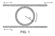
- FIG. 1 The basic form of the planar waveguide ring resonator is shown schematically in Figure 1 .
- a ring of waveguide material is positioned in a coupling arrangement with two straight waveguide sections, as shown, such that there is a small gap, typically 0.1 to 1 ⁇ m between the ring and the straight sections at their closest approach.
- Polychromatic light, S in enters from the left and travels along the upper straight section. As it passes the point of proximity to the ring light is coupled across into the ring through the mechanism of evanescent field coupling.
- the ring only supports a particular frequency of light, known as the 'resonant frequency'. This occurs when the length of the ring is a whole number of wavelengths of the light propagating round it.
- Each value of K therefore corresponds to a different longitudinal mode of the resonator, where there will be an integral number of wavelengths in the ring.
- the FSR of the ring resonator should be greater than the entire DWDM band - typically about a 30nm band - to prevent cross-talk.
- the FSR be 30nm (3750GHz at around 1550nm), and assume n e is 3.5 for silicon.
- Solving (2) for R gives a required radius of 3.6um.
- the index difference between the core and cladding materials needs be large so as to tightly confine the propagating mode.
- Finesse FSR ⁇ ⁇ f
- ⁇ f the full-width at half maximum (FWHM) of the resonant peak.
- the FWHM, or passband, of an add/drop device defines the range of frequencies that may be added or dropped. If the FWHM is made too narrow, corresponding to a very high Finesse, then it is possible that the whole width of the required channel may not be selected and some light will remain in the main signal stream. This is deleterious for two reasons, (a) the dropped signal will be reduced in amplitude, and (b) if the same frequency is to be later added to the signal stream then cross-talk could result. If the FWHM is too wide then light from neighbouring channels may be extracted along with the required channel, leading to cross-talk.
- the passband is proportional to the square of the coupling coefficient, ⁇ .
- the required passband be 0.4nm, then from (4) the required coupling coefficient would be 20%.
- the Quality Factor, Q is the ratio of the time averaged power stored in the ring per cycle to the power coupled, or scattered, out of the ring.
- the Quality Factor was limited to 250 due to the straight and curved sections fusing together during manufacture, which greatly increased the coupling coefficient.
- a feature of a highly curved waveguide is that the propagating mode ceases to make contact with the inside edge of the guide and becomes what is known as a 'whispering gallery' mode. In geometrical terms, it reflects from only the outside edge of the guide as it propagates round the bend. It will be obvious that, in this case, the inner edge of the ring resonator is redundant and so the ring may be replaced by a disk of uniform index.
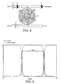
- Figure 2 schematically illustrates a disk (rather than a ring as in Figure 1 ) resonator in a non-resonant condition.
- input light at the non-resonant wavelength ⁇ 1 passes straight through the device without being coupled to the disk 10.
- input light at the resonant wavelength ⁇ 2 is coupled into the disk 10 and so is not present at the throughput output.
- Figure 4 schematically illustrates such a resonator used as a channel drop filter.
- ⁇ 1 is indicative in a generic sense of non-resonant wavelengths
- ⁇ 2 is indicative in a generic sense of resonant wavelengths.
- light at ⁇ 1 is not coupled to the disk 10 and passes to the throughput output, and light at ⁇ 2 is coupled via the disk to the second waveguide 20 where it emerges (in a reverse direction) at the drop output.
- Figure 5 schematically illustrates the wavelength response of the device of Figure 4 , where light at the throughput output is represented by a dotted response curve and light at the drop output is represented by a solid response curve, on an arbitrary normalised scale on the vertical axis.
- the resonant condition at which light is transferred from the input to the drop port occurs as a series of peaks, the width of which depends on the finesse of the device, the peaks being separated by the free spectral range (FSR) as described above.
- FSR free spectral range
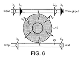
- Figure 6 schematically illustrates the use of a resonator as a channel add/drop multiplexer.
- This operation is basically similar to the device of Figure 4 , except that a wavelength channel to be added is supplied as an input to the second waveguide 20.
- This "add" wavelength channel is at a wavelength ⁇ 2 ', indicative in a generic sense of resonant wavelengths of the resonator 10.
- the channel to be added may be at the same wavelength as the input channel to be dropped, or maybe at another resonant wavelength of the device.
- the notation ⁇ 2 ' is simply used to indicate that the channel to be added will contain different information to the channel ⁇ 2 to be dropped.
- the ring or disk-type structure of the resonator cavity 10 is formed of a polymer material.
- the reason for using such a material is to allow the refractive index of the resonator cavity, and therefore the coupling wavelengths for coupling of light between the waveguides and the resonator cavity, to be varied by changing the temperature of the resonator cavity.
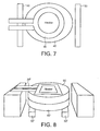
- Figure 7 schematically illustrates an electrical heater element 30 formed over a resonator 40 having laterally adjacent input and output waveguides 50 for coupling into and out of the resonator cavity 40.
- the heater element 30 may be formed of a deposited electrically resistant conductor such as Nichrome.
- Figure 8 shows a similar arrangement in which an electrical heating element 30' is formed on a polymer cladding 60 overlying a polymer resonator cavity 40'. Input and output waveguides 50' are fabricated beneath the resonant cavity 40'.
- the input and output waveguides could be laterally adjacent to the resonant cavity and/or arranged so that the resonant cavity and the waveguides at least partly overlie one another, that is to say that the waveguides are disposed out of the plane of the resonant cavity.
- the waveguides are shown below the resonant cavity (assuming that the substrate, by convention, would be drawn at the bottom of Figure 8 )
- the waveguides could in fact be formed over the resonant cavity.
- combinations of the above arrangements could be used so that, for example, one waveguide is formed laterally adjacent to a resonant cavity and another out of the plane of the resonant cavity but at least partly overlying it, and so on.
- the heating element 30, 30' shown in Figures 7 and 8 could of course be replaced or augmented by a cooling element such as an electrical Peltier element to provide a different range of temperature adjustment.
- Figure 9 schematically illustrates a temperature response of the above device using a heating and/or cooling arrangement to vary the temperature of a polymer resonant cavity.
- the device exhibits a peaked response as before (with only the channel drop response being shown for clarity of the diagram) but the peaks may be translated within the wavelength range according to the temperature of the polymer from for example 0 to 60 degrees Celsius. Over this range of temperature and using an example set of device parameters, it can be seen that a variation in the peak position of about half of the free spectral range of the device can be obtained.
- a particular wavelength channel can be made to pass straight through the device (at a non-resonant condition) or to be dropped by the device (at a resonant condition).
- a control loop (not shown) may be established using an optical detector at the output (drop) port and a conventional negative feedback arrangement to the heating and/or cooling arrangement so that a substantially maximised output response may be obtained at the drop port.
- Figure 10 schematically illustrates the fabrication of a channel and/drop multiplexer.
- a number of layers of material are deposited on a substrate.
- the overall structure is therefore as follows:
- the polymer disk 78 is surrounded by an air (or at least non-solid) cladding 86. This provides a greater index difference between the disk and its lateral surroundings, so that bending losses in the disk are reduced.
- Suitable materials for the ring or disk cavity include silicone resin, polysilioxane, halogenated silicone resin, halogenated polysilioxane, polyamides, polycarbonates or the like.
- the rate of change of refractive index for these materials with respect to temperature (dn/dT) is of the order of -1 x 10 -4 to -5 x 10 -5 per degree Celsius. This compares with a much smaller and positive dn/dT for typical glass materials of the order of +1 x 10 -5 .
- the much larger magnitude and opposite sense dn/dT for the polymer material means that the heating of the cavity does not have to be completely localised to the cavity - in fact, depending on whether other polymer features requiring independent responses are formed on the same device, the entire device could even be heated or cooled to effect a temperature change of the cavity and so vary its coupling response.
- Figures 11 and 12 are schematic side and perspective views of an optically heated device.
- each of one or more resonant cavities 100 (or other temperature-variable optical devices) formed on a substrate 110 is heatable by an optical element 120 such as a laser device.
- the arrangement of cavities and elements is flexible, in that there may be provided a respective element 120 for each of the heatable cavities 100, two or more elements 120 may be provided for a single cavity 100, or two or more cavities may be heated by a common element if a common mode or tracked response is required.
- the heating devices 120 are mounted on a separate mounting arrangement, which may even be a separate substrate 130, which overlies the substrate 110 carrying the heatable devices 100.
- the two substrates may be aligned using conventional micro electro-mechanical (MEMS) formations such as interengaging protrusions and recesses in the two substrates.
- MEMS micro electro-mechanical
- the heating elements 120 may be driven by electrical signals generated by control electronics 140.
- An advantage of this arrangement is that the electrical connections and the heating devices 120 are not formed on the substrate 110 carrying the temperature-sensitive optically active devices (e.g. cavities) 100, which therefore allows the optically active devices 100 to be positioned closer to one another because space does not need to be allocated on the substrate 100 for electrical wiring and the like.
- FIG. 13 schematically illustrates the use of a channel add/drop multiplexer 200 within an optical telecommunication system.
- the optical telecommunication system comprises a so-called backbone or trunk communication structure connected via a wide area network (WAN) to a user within a local area network (LAN).
- WAN wide area network
- LAN local area network
- a typical user 210 generates and receives traffic at a user wavelength ⁇ 1 via an optical transmitter/receiver 220.
- ⁇ 1 is passed from the LAN to the WAN by a wavelength switch 230. It is then routed into the backbone structure via an add/drop multiplexer 200 to form one of many channels switched by optical cross connects (OXC) 240.
- OXC optical cross connects
- Figure 14 schematically illustrates a double-disk (or ring) device having a series resonator arrangement.
- the drawing shows a ring structure, of course disks could be used, or annuli with smaller openings in the middle, and so on.
- a double disk arrangement is shown, another plural number of disks could of course be used, with the multiple disks arranged in a series-coupling sense or a series/parallel coupling sense.
- the basic configuration of the double-ring resonator is that light S in couples from an input waveguide 300 into an upper ring 310 of radius R2, and propagates in a clockwise direction, similar to the single ring resonator. At the point where the two rings approach one other light is coupled into a second ring 320 of radius R1, and travels in an anti-clockwise direction. Finally light is coupled into an output waveguide and exits (S fil ) towards the right, all directions being simply as shown in the Figure.
- the radii R1 and R2 can be made to be different so that the free spectral ranges of the two resonators are different.
- N and M are natural and coprime numbers (i.e. not having a common divisor).
- the effect is to increase the free spectral range of the overall resonator arrangement compared to that of either individual cavity. This is equivalent to that of Moiré fringes caused by superimposed grids of differing pitch (e.g. net curtains). This principle is sometimes known as the 'Vernier effect'.
- the disk radii and/or other properties can be arranged so as to give substantially the same wavelength response.
- the finesse of the arrangement is greater than that of any individual one of the resonator cavities.
- the actual coupling peak of the combined arrangement depends on the overlap of respective peaks from the multiply resonators.
- small changes can have large effects.
- a small error in the tuning of one resonator can mean that the wrong two peaks overlap and the response of the arrangement is dramatically incorrect.
- FIG. 15 schematically illustrates an electrical heating/cooling arrangement for a two-disk system, in which control electronics 332 provides independent control for heating elements 334, 336 relevant to two resonator disks 335, 337.
- Figure 16 schematically illustrates a double-disk system having a parallel resonator arrangement.
- the disks may be nominally identical or may have deliberately different properties such as different FSRs, as described above with reference to Figure 14 .
- a heating/cooling arrangement is used to adjust the responses of the resonator cavities, which are preferably fabricated from a polymer material.
- the resonant wavelength of the cavities matches the wavelength of incoming light
- light entering via the Input port is at least partially coupled into a first resonator 302 and coupled out to the Drop port.
- Any light remaining in the Input waveguide, or coupled back into the Input waveguide from the first waveguide 302, may be at least partially coupled into a second resonator 304 and back into the Drop port, and so on.
- Input light at wavelengths which are not coupled into the resonators emerges at the Throughput port.
- the first resonator 302 acts to couple a large part of this light into the Drop port to give a power at the Drop port of, say, -5dB and a lower proportion, say -15dB, propagating in the direction of the Throughput port.
- a further transfer occurs at the second resonator 304 resulting in a signal at -30dB emerging at the Throughput port.
- the second resonator contributes - 20dB to the signal heading towards the Drop port, but this is in turn coupled over with an extinction of -15dB giving an effective power of -35dB heading towards the Throughput port.
- Figure 17 schematically illustrates the fabrication of a channel and/drop multiplexer using a polymer material for the resonator cavities. For clarity of the diagram, as it is a side view only one cavity and one waveguide have been shown. In the fabrication process used to create the waveguide and cavity arrangement, a number of layers of material are deposited on a substrate. The overall structure is therefore as follows:
- the polymer disk 78 is surrounded by an air (or at least non-solid) cladding 86. This provides a greater index difference between the disk and its lateral surroundings, so that bending losses in the disk are reduced.
- Suitable materials for the ring or disk cavity include silicone resin, polysilioxane, halogenated silicone resin, halogenated polysilioxane, polyamides, polycarbonates or the like.
- the rate of change of refractive index for these materials with respect to temperature is of the order of -1 x 10 -4 to -5 x 10 -5 per degree Celsius. This compares with a much smaller and positive dn/dT for typical glass materials of the order of +1 x 10 -5 .
- the much larger magnitude and opposite sense dn/dT for the polymer material means that the heating of the cavity does not have to be completely localised to the cavity - in fact, depending on whether other polymer features requiring independent responses are formed on the same device, the entire device could even be heated or cooled to effect a temperature change of the cavity and so vary its coupling response.
- FIG 18 schematically illustrates a resonator arrangement using bendmode to whispering gallery mode (WGM) coupling.
- WGM whispering gallery mode
- Two waveguides 600 are shown, each of which lies outside of the plane of the circular resonator 610 (i.e. vertical coupling is used).
- the waveguides are curved over a coupling region, preferably so as to follow the outer shape of the resonator.
- Figure 19 schematically illustrates a resonator arrangement using WGM to WGM coupling.
- the waveguides 620 are curved as in Figure 18 , but are also widened in the plane of the circular resonator 630 over a part of a coupling region. The transition to a widened cross-section allows WGMs to propagate in the waveguide, so allowing WGM to WGM coupling between the waveguide and the resonator.
- the lateral peripheral edges of the resonator and of the waveguide are bounded by a large refractive index difference, e.g. being adjacent to an air gap.
- a large refractive index difference e.g. being adjacent to an air gap.
- providing the air interface can reduce bending losses in the curved waveguide sections.
- air is used here in a very general sense to distinguish over a solid or liquid material adjacent to the waveguide. In a real fabrication, the skilled man will of course realise that the "air gap" could be filled by atmospheric air, gases used during the fabrication process, a deliberately introduced gas or gas mixture, or even a partial or substantially full vacuum.
- FIG 20 is a schematic diagram of a device using an arrayed waveguide grating (AWG) with multiple resonators.
- AMG arrayed waveguide grating
- the AWG allows the 30 nm range useable in systems having Erbium doped amplification (as an example) to be split into smaller wavelength ranges of, for example, up to 5 nm each, for separate handling by a resonator type device.
- an input optical signal is supplied to an AWG 700.
- the AWG acts as a wavelength separator to divide the input optical signal into separate wavelength channel output signals 710.
- Each of these is supplied to a resonator arrangement 720.
- the resonator arrangement is shown for simplicity in Figure 20 as a single resonator, but can of course be any other resonator arrangement such as other arrangements described in the present specification.
- each resonator arrangement At the output of each resonator arrangement is an optical signal within a reduced wavelength band compared to the band available for the input optical signal. If there is a need to recombine these bands into a single output optical signal then another AWG could of course be used. However, a particularly convenient way of achieving this with a single AWG is described below. This has the advantage of reducing the chip area required to fabricate the device, as AWGs tend to be rather large devices by the standards of integrated optical fabrication.
- FIG 21 is a schematic diagram of a device using an AWG coupled to a multiple resonator/reflector arrangement.
- an input optical signal supplied via a circulator 730, is again split into multiple wavelength channels by the AWG.
- Each separate wavelength channel is then processed by a respective resonator arrangement, again shown as a single resonator in this diagram for simplicity.
- the output from each resonator arrangement is reflected by a high reflectivity (HR) mirror 740, through the resonator arrangement and back through the AWG.
- HR high reflectivity
- the AWG acts to recombine the wavelength channels into a single optical output signal at the output port of the circulator.
Landscapes
- Physics & Mathematics (AREA)
- Nonlinear Science (AREA)
- General Physics & Mathematics (AREA)
- Optics & Photonics (AREA)
- Optical Integrated Circuits (AREA)
- Aiming, Guidance, Guns With A Light Source, Armor, Camouflage, And Targets (AREA)
- Wire Bonding (AREA)
- Photo Coupler, Interrupter, Optical-To-Optical Conversion Devices (AREA)
- Communication Control (AREA)
- Surgical Instruments (AREA)
- Radar Systems Or Details Thereof (AREA)
- Semiconductor Lasers (AREA)
Claims (26)
- Dispositif de traitement de signal optique intégré, comprenant :un substrat (70) ;un guide d'ondes guidant la lumière (300) formé dans ou sur le substrat, le guide d'ondes étant conçu pour transporter un signal optique d'entrée, caractérisé en ce qu'il comprend :une région formant cavité de résonateur (78) formée dans ou sur le substrat, constituée d'un matériau ayant un taux de variation de l'indice de réfraction avec la température d'amplitude supérieure à celui du matériau du substrat ou du guide d'ondes, la région de résonateur étant adjacente au guide d'ondes de façon à permettre un couplage optique entre le guide d'ondes et la région de résonateur à une ou plusieurs longueurs d'onde de couplage ; etun système de chauffage et/ou de refroidissement (100, 120) pouvant être mis en oeuvre pour faire varier la température d'au moins la région de résonateur afin de provoquer une variation correspondante des longueurs d'onde de couplage.
- Dispositif selon la revendication 1, dans lequel la région de résonateur est une région sensiblement plane.
- Dispositif selon la revendication 2, dans lequel la région de résonateur est une région globalement circulaire.
- Dispositif selon la revendication 3, dans lequel la région de résonateur est une région en forme de disque.
- Dispositif selon la revendication 2, dans lequel la région de résonateur est une région globalement elliptique.
- Dispositif selon l'une quelconque des revendications 2 à 5, dans lequel le guide d'ondes n'est pas disposé dans le plan de la région de résonateur.
- Dispositif selon la revendication 6, dans lequel la région de résonateur et le guide d'ondes sont formés de façon à être superposés, au moins en partie, l'un sur l'autre.
- Dispositif selon la revendication 6 ou 7, dans lequel la région de résonateur est délimitée, dans le plan de la région de résonateur, par un interstice d'air.
- Dispositif selon l'une quelconque des revendications précédentes, dans lequel la région de résonateur est formée d'un matériau polymère.
- Dispositif selon l'une quelconque des revendications précédentes, dans lequel le système de chauffage et/ou de refroidissement comprend au moins un élément chauffant électrique.
- Dispositif selon l'une quelconque des revendications précédentes, dans lequel le système de chauffage et/ou de refroidissement comprend au moins un dispositif de chauffage optique.
- Dispositif selon la revendication 10, dans lequel le système de chauffage optique comprend un ou plusieurs dispositif(s) à laser conçu(s) pour irradier au moins la région de résonateur.
- Dispositif selon l'une quelconque des revendications précédentes, dans lequel le système de chauffage et/ou de refroidissement comprend au moins un élément Peltier.
- Dispositif selon l'une quelconque des revendications précédentes, comprenant une couche de gaine polymère disposée sur la région de résonateur.
- Dispositif selon l'une quelconque des revendications précédentes, comprenant au moins un deuxième guide d'ondes guidant la lumière formé dans ou sur le substrat à proximité immédiate de la région de résonateur de façon à permettre un couplage optique entre le guide d'ondes et la région de résonateur à une ou plusieurs longueurs d'onde de couplage.
- Dispositif de traitement de signal optique comprenant :un dispositif de séparation de longueur d'onde pour séparer un signal optique d'entrée en au moins deux canaux de longueurs d'onde ; etdeux ou plusieurs dispositifs de traitement de signal optique selon l'une quelconque des revendications précédentes, chacun conçu pour traiter l'un, respectif, des canaux de longueur d'onde.
- Dispositif selon la revendication 16, dans lequel le dispositif de séparation de longueur d'onde est un réseau sélectif planaire.
- Dispositif selon la revendication 16 ou 17, comprenant un réflecteur respectif associé au dispositif de traitement de signal optique traitant chaque canal de longueur d'onde de façon à rétroréfléchir la lumière vers le dispositif de séparation de longueur d'onde.
- Dispositif selon l'une quelconque des revendications précédentes, comprenant un système résonateur ayant deux ou plusieurs régions formant cavités de résonateur formées d'un matériau polymère dans ou sur le substrat et optiquement couplées pour permettre le transfert de signaux optiques entre les régions formant cavités de résonateur, le système résonateur étant à proximité immédiate du guide d'ondes de façon à permettre un couplage optique entre le guide d'ondes et le système résonateur à une ou plusieurs longueurs d'onde de couplage.
- Dispositif selon la revendication 19, dans lequel le système résonateur comprend un agencement en série de deux ou plusieurs cavités de résonateur afin que, lors de l'utilisation, de la lumière puisse être couplée :entre le guide d'ondes guidant la lumière et une première cavité de résonateur dans l'agencement en série ;entre la première cavité de résonateur et une autre cavité de résonateur dans l'agencement en série ; etentre la cavité de résonateur supplémentaire et un deuxième guide d'ondes guidant la lumière.
- Dispositif selon la revendication 19, dans lequel le système résonateur comprend un agencement en parallèle de deux ou plusieurs cavités de résonateur reliant le guide d'ondes guidant la lumière au deuxième guide d'ondes guidant la lumière afin que de la lumière puisse être couplée en même temps entre le guide d'ondes guidant la lumière et un deuxième guide d'ondes guidant la lumière par l'intermédiaire de deux ou plusieurs cavités de résonateur.
- Dispositif selon l'une quelconque des revendications précédentes, dans lequel le guide d'ondes suit un trajet sensiblement incurvé sur au moins une partie d'une zone de couplage dans laquelle de la lumière peut être couplée entre le guide d'ondes et le résonateur.
- Dispositif selon la revendication 22, dans lequel un bord latéral extérieur du guide d'ondes est délimité par un interstice d'air.
- Dispositif selon la revendication 22 ou 23, dans lequel la superficie en section transversale du guide d'ondes est augmentée sur au moins une partie de la zone de couplage dans laquelle de la lumière peut être couplée entre le guide d'ondes et le résonateur.
- Dispositif selon la revendication 24, dans lequel la superficie en section transversale est augmentée dans le plan du résonateur.
- Système de communication optique comprenant un ou plusieurs dispositifs de traitement de signal optique selon l'une quelconque des revendications précédentes.
Applications Claiming Priority (3)
| Application Number | Priority Date | Filing Date | Title |
|---|---|---|---|
| GB0114648A GB2376532A (en) | 2001-06-15 | 2001-06-15 | Thermally controlled optical resonator |
| GB0114648 | 2001-06-15 | ||
| PCT/GB2002/002736 WO2002103448A2 (fr) | 2001-06-15 | 2002-06-14 | Dispositif de maniement de signal optique integre |
Publications (2)
| Publication Number | Publication Date |
|---|---|
| EP1423751A2 EP1423751A2 (fr) | 2004-06-02 |
| EP1423751B1 true EP1423751B1 (fr) | 2008-08-27 |
Family
ID=9916682
Family Applications (1)
| Application Number | Title | Priority Date | Filing Date |
|---|---|---|---|
| EP02735621A Expired - Lifetime EP1423751B1 (fr) | 2001-06-15 | 2002-06-14 | Dispositif de maniement de signal optique integre |
Country Status (6)
| Country | Link |
|---|---|
| US (1) | US20090226129A1 (fr) |
| EP (1) | EP1423751B1 (fr) |
| AT (1) | ATE406598T1 (fr) |
| DE (1) | DE60228591D1 (fr) |
| GB (1) | GB2376532A (fr) |
| WO (1) | WO2002103448A2 (fr) |
Cited By (1)
| Publication number | Priority date | Publication date | Assignee | Title |
|---|---|---|---|---|
| DE102015206847A1 (de) * | 2015-04-16 | 2016-10-20 | Technische Universität Berlin | Optoelektronisches Bauelement mit Resonator |
Families Citing this family (21)
| Publication number | Priority date | Publication date | Assignee | Title |
|---|---|---|---|---|
| DE10065723A1 (de) * | 2000-12-29 | 2002-07-04 | Bosch Gmbh Robert | Anordnung zur Temperaturmessung und -regelung |
| CA2550678C (fr) * | 2003-12-24 | 2013-03-19 | Pirelli & C. S.P.A. | Dispositif resonateur en micro-anneau a faibles pertes |
| TWI251393B (en) * | 2004-03-31 | 2006-03-11 | Nec Corp | Tunable laser |
| US7231113B2 (en) | 2005-08-19 | 2007-06-12 | Infinera Corporation | Coupled optical waveguide resonators with heaters for thermo-optic control of wavelength and compound filter shape |
| JP5050548B2 (ja) | 2007-02-07 | 2012-10-17 | 日本電気株式会社 | 光モジュール |
| US7657129B2 (en) * | 2007-09-04 | 2010-02-02 | Lockheed Martin Corporation | Optical focal plane data coupler |
| US8594471B2 (en) | 2011-03-30 | 2013-11-26 | Telefonaktiebolaget L M Ericsson (Publ) | Adaptive waveguide optical switching system and method |
| CN104067162A (zh) * | 2012-01-31 | 2014-09-24 | 富士通株式会社 | 光发送器及光发送器的控制方法 |
| US9081215B1 (en) * | 2012-02-16 | 2015-07-14 | Sandia Corporation | Silicon photonic heater-modulator |
| US20140029954A1 (en) * | 2012-07-30 | 2014-01-30 | Commscope, Inc. Of North Carolina | Systems for Transmitting Control Signals Over a Fiber Optic Data Network and Related Methods and Apparatus |
| US9118413B2 (en) * | 2012-12-20 | 2015-08-25 | Nokia Technologies Oy | Apparatus and a method |
| EP3058629B1 (fr) | 2013-10-15 | 2022-06-08 | Hewlett Packard Enterprise Development LP | Résonateur optique à modulation de couplage |
| US10090632B2 (en) | 2014-02-28 | 2018-10-02 | Hewlett Packard Enterprise Development Lp | Lasing output based on varying modal index |
| US9212912B1 (en) | 2014-10-24 | 2015-12-15 | Honeywell International Inc. | Ring laser gyroscope on a chip with doppler-broadened gain medium |
| JP6346994B2 (ja) * | 2014-10-29 | 2018-06-20 | 華為技術有限公司Huawei Technologies Co.,Ltd. | 光分岐挿入装置および光ネットワーク信号伝送方法 |
| US10644808B2 (en) * | 2017-08-23 | 2020-05-05 | Seagate Technology Llc | Silicon photonics based optical network |
| US11405112B2 (en) * | 2017-12-28 | 2022-08-02 | Futurewei Technologies, Inc. | Wavelength division multiplexed optical parameter detection receiver |
| CN109186641B (zh) * | 2018-08-01 | 2022-03-11 | 中国电子科技集团公司第十一研究所 | 一种制造光纤传感器的方法、及光纤传感器 |
| US11372269B2 (en) * | 2018-08-17 | 2022-06-28 | International Business Machines Corporation | Silicon photonic tunable device with thermo-optic channel |
| US11733455B2 (en) * | 2019-04-02 | 2023-08-22 | The Trustees Of Columbia University In The City Of New York | Amplitude and phase light modulator based on miniature optical resonators |
| DE102022109218A1 (de) | 2022-04-14 | 2023-10-19 | Ams-Osram International Gmbh | Laseranordnung Und Verfahren Zum Betreiben Einer Laseranordnung |
Family Cites Families (7)
| Publication number | Priority date | Publication date | Assignee | Title |
|---|---|---|---|---|
| WO1986002171A1 (fr) * | 1984-10-01 | 1986-04-10 | Polaroid Corporation | Amplificateur et laser a guide d'ondes optique |
| US4782492A (en) * | 1986-05-05 | 1988-11-01 | Polaroid Corporation | Thermally controllable optical devices and system |
| US5398256A (en) * | 1993-05-10 | 1995-03-14 | The United States Of America As Represented By The United States Department Of Energy | Interferometric ring lasers and optical devices |
| WO2000050938A1 (fr) * | 1999-02-22 | 2000-08-31 | Massachusetts Institute Of Technology | Resonateurs optiques couples verticalement utilisant une architecture de guides d'ondes en grille croisee |
| US6243517B1 (en) * | 1999-11-04 | 2001-06-05 | Sparkolor Corporation | Channel-switched cross-connect |
| WO2001038905A2 (fr) * | 1999-11-23 | 2001-05-31 | Nanovation Technologies, Inc. | Accord thermique localise de resonateurs annulaires |
| JP2002072260A (ja) * | 2000-08-31 | 2002-03-12 | Oki Electric Ind Co Ltd | 光スイッチ素子及び波長ルータ |
-
2001
- 2001-06-15 GB GB0114648A patent/GB2376532A/en not_active Withdrawn
-
2002
- 2002-06-14 US US10/481,051 patent/US20090226129A1/en not_active Abandoned
- 2002-06-14 EP EP02735621A patent/EP1423751B1/fr not_active Expired - Lifetime
- 2002-06-14 WO PCT/GB2002/002736 patent/WO2002103448A2/fr active IP Right Grant
- 2002-06-14 DE DE60228591T patent/DE60228591D1/de not_active Expired - Fee Related
- 2002-06-14 AT AT02735621T patent/ATE406598T1/de not_active IP Right Cessation
Cited By (2)
| Publication number | Priority date | Publication date | Assignee | Title |
|---|---|---|---|---|
| DE102015206847A1 (de) * | 2015-04-16 | 2016-10-20 | Technische Universität Berlin | Optoelektronisches Bauelement mit Resonator |
| US10025030B2 (en) | 2015-04-16 | 2018-07-17 | Technische Universitaet Berlin | Optoelectronic component having a resonator |
Also Published As
| Publication number | Publication date |
|---|---|
| ATE406598T1 (de) | 2008-09-15 |
| GB0114648D0 (en) | 2001-08-08 |
| WO2002103448A2 (fr) | 2002-12-27 |
| WO2002103448A3 (fr) | 2003-06-19 |
| GB2376532A (en) | 2002-12-18 |
| DE60228591D1 (de) | 2008-10-09 |
| EP1423751A2 (fr) | 2004-06-02 |
| US20090226129A1 (en) | 2009-09-10 |
Similar Documents
| Publication | Publication Date | Title |
|---|---|---|
| EP1423751B1 (fr) | Dispositif de maniement de signal optique integre | |
| EP1226461B1 (fr) | Phasar a bandes passantes aplaties | |
| US6785430B2 (en) | Method and apparatus for integrating an optical transmit module | |
| Okamoto | Recent progress of integrated optics planar lightwave circuits | |
| US20070280326A1 (en) | External cavity laser in thin SOI with monolithic electronics | |
| US6259847B1 (en) | Optical communication system including broadband all-pass filter for dispersion compensation | |
| US20020197013A1 (en) | Method and apparatus for tuning a laser with a bragg grating in a semiconductor substrate | |
| US10261260B2 (en) | Tunable microring resonator | |
| Offrein et al. | Resonant coupler-based tunable add after-drop filter in silicon-oxynitride technology for WDM networks | |
| US7245792B2 (en) | Silicon-based tunable single passband optical filter | |
| US20020126291A1 (en) | Spectrum division multiplexing for high channel count optical networks | |
| US6900930B2 (en) | Method and apparatus of a semiconductor-based gain equalization device for optical amplifiers | |
| US6856732B2 (en) | Method and apparatus for adding/droping optical signals in a semiconductor substrate | |
| EP1065813A2 (fr) | Système optique | |
| US20050068602A1 (en) | Optical add-filtering switching device | |
| US7200302B2 (en) | Planar lightwave Fabry-Perot filter | |
| US6590684B1 (en) | Optical system | |
| EP0857314A1 (fr) | Dispositifs optiques selectifs en longueurs d'ondes | |
| CN112005507B (zh) | 具有低功耗的可重新配置光分插多路复用器 | |
| WO2002079863A2 (fr) | Filtres optoelectroniques | |
| US20060140541A1 (en) | Integrated optical device | |
| JP5895558B2 (ja) | 光伝送システム | |
| Huang et al. | A coupled-waveguide grating resonator filter | |
| WO2018022296A1 (fr) | Filtres optiques athermiques reconfigurables | |
| Mizuno et al. | Uniform wavelength spacing Mach-Zehnder interferometer using phase-generating couplers |
Legal Events
| Date | Code | Title | Description |
|---|---|---|---|
| PUAI | Public reference made under article 153(3) epc to a published international application that has entered the european phase |
Free format text: ORIGINAL CODE: 0009012 |
|
| 17P | Request for examination filed |
Effective date: 20031222 |
|
| AK | Designated contracting states |
Kind code of ref document: A2 Designated state(s): AT BE CH CY DE DK ES FI FR GB GR IE IT LI LU MC NL PT SE TR |
|
| RAP1 | Party data changed (applicant data changed or rights of an application transferred) |
Owner name: GEMFIRE EUROPE LIMITED |
|
| GRAP | Despatch of communication of intention to grant a patent |
Free format text: ORIGINAL CODE: EPIDOSNIGR1 |
|
| GRAS | Grant fee paid |
Free format text: ORIGINAL CODE: EPIDOSNIGR3 |
|
| GRAA | (expected) grant |
Free format text: ORIGINAL CODE: 0009210 |
|
| AK | Designated contracting states |
Kind code of ref document: B1 Designated state(s): AT BE CH CY DE DK ES FI FR GB GR IE IT LI LU MC NL PT SE TR |
|
| REG | Reference to a national code |
Ref country code: GB Ref legal event code: FG4D |
|
| REG | Reference to a national code |
Ref country code: CH Ref legal event code: EP |
|
| REG | Reference to a national code |
Ref country code: IE Ref legal event code: FG4D |
|
| REF | Corresponds to: |
Ref document number: 60228591 Country of ref document: DE Date of ref document: 20081009 Kind code of ref document: P |
|
| PG25 | Lapsed in a contracting state [announced via postgrant information from national office to epo] |
Ref country code: ES Free format text: LAPSE BECAUSE OF FAILURE TO SUBMIT A TRANSLATION OF THE DESCRIPTION OR TO PAY THE FEE WITHIN THE PRESCRIBED TIME-LIMIT Effective date: 20081208 Ref country code: NL Free format text: LAPSE BECAUSE OF FAILURE TO SUBMIT A TRANSLATION OF THE DESCRIPTION OR TO PAY THE FEE WITHIN THE PRESCRIBED TIME-LIMIT Effective date: 20080827 |
|
| PG25 | Lapsed in a contracting state [announced via postgrant information from national office to epo] |
Ref country code: FI Free format text: LAPSE BECAUSE OF FAILURE TO SUBMIT A TRANSLATION OF THE DESCRIPTION OR TO PAY THE FEE WITHIN THE PRESCRIBED TIME-LIMIT Effective date: 20080827 Ref country code: AT Free format text: LAPSE BECAUSE OF FAILURE TO SUBMIT A TRANSLATION OF THE DESCRIPTION OR TO PAY THE FEE WITHIN THE PRESCRIBED TIME-LIMIT Effective date: 20080827 |
|
| PG25 | Lapsed in a contracting state [announced via postgrant information from national office to epo] |
Ref country code: BE Free format text: LAPSE BECAUSE OF FAILURE TO SUBMIT A TRANSLATION OF THE DESCRIPTION OR TO PAY THE FEE WITHIN THE PRESCRIBED TIME-LIMIT Effective date: 20080827 |
|
| PG25 | Lapsed in a contracting state [announced via postgrant information from national office to epo] |
Ref country code: DK Free format text: LAPSE BECAUSE OF FAILURE TO SUBMIT A TRANSLATION OF THE DESCRIPTION OR TO PAY THE FEE WITHIN THE PRESCRIBED TIME-LIMIT Effective date: 20080827 |
|
| PG25 | Lapsed in a contracting state [announced via postgrant information from national office to epo] |
Ref country code: PT Free format text: LAPSE BECAUSE OF FAILURE TO SUBMIT A TRANSLATION OF THE DESCRIPTION OR TO PAY THE FEE WITHIN THE PRESCRIBED TIME-LIMIT Effective date: 20090127 |
|
| PLBE | No opposition filed within time limit |
Free format text: ORIGINAL CODE: 0009261 |
|
| STAA | Information on the status of an ep patent application or granted ep patent |
Free format text: STATUS: NO OPPOSITION FILED WITHIN TIME LIMIT |
|
| 26N | No opposition filed |
Effective date: 20090528 |
|
| PG25 | Lapsed in a contracting state [announced via postgrant information from national office to epo] |
Ref country code: SE Free format text: LAPSE BECAUSE OF FAILURE TO SUBMIT A TRANSLATION OF THE DESCRIPTION OR TO PAY THE FEE WITHIN THE PRESCRIBED TIME-LIMIT Effective date: 20081127 Ref country code: MC Free format text: LAPSE BECAUSE OF NON-PAYMENT OF DUE FEES Effective date: 20090630 |
|
| REG | Reference to a national code |
Ref country code: CH Ref legal event code: PL |
|
| REG | Reference to a national code |
Ref country code: FR Ref legal event code: ST Effective date: 20100226 |
|
| REG | Reference to a national code |
Ref country code: IE Ref legal event code: MM4A |
|
| PG25 | Lapsed in a contracting state [announced via postgrant information from national office to epo] |
Ref country code: LI Free format text: LAPSE BECAUSE OF NON-PAYMENT OF DUE FEES Effective date: 20090630 Ref country code: IE Free format text: LAPSE BECAUSE OF NON-PAYMENT OF DUE FEES Effective date: 20090614 Ref country code: CH Free format text: LAPSE BECAUSE OF NON-PAYMENT OF DUE FEES Effective date: 20090630 Ref country code: FR Free format text: LAPSE BECAUSE OF NON-PAYMENT OF DUE FEES Effective date: 20090630 |
|
| PG25 | Lapsed in a contracting state [announced via postgrant information from national office to epo] |
Ref country code: DE Free format text: LAPSE BECAUSE OF NON-PAYMENT OF DUE FEES Effective date: 20100101 |
|
| PG25 | Lapsed in a contracting state [announced via postgrant information from national office to epo] |
Ref country code: GR Free format text: LAPSE BECAUSE OF FAILURE TO SUBMIT A TRANSLATION OF THE DESCRIPTION OR TO PAY THE FEE WITHIN THE PRESCRIBED TIME-LIMIT Effective date: 20081128 |
|
| PG25 | Lapsed in a contracting state [announced via postgrant information from national office to epo] |
Ref country code: IT Free format text: LAPSE BECAUSE OF NON-PAYMENT OF DUE FEES Effective date: 20090614 |
|
| PG25 | Lapsed in a contracting state [announced via postgrant information from national office to epo] |
Ref country code: LU Free format text: LAPSE BECAUSE OF NON-PAYMENT OF DUE FEES Effective date: 20090614 |
|
| PG25 | Lapsed in a contracting state [announced via postgrant information from national office to epo] |
Ref country code: TR Free format text: LAPSE BECAUSE OF FAILURE TO SUBMIT A TRANSLATION OF THE DESCRIPTION OR TO PAY THE FEE WITHIN THE PRESCRIBED TIME-LIMIT Effective date: 20080827 |
|
| PG25 | Lapsed in a contracting state [announced via postgrant information from national office to epo] |
Ref country code: CY Free format text: LAPSE BECAUSE OF FAILURE TO SUBMIT A TRANSLATION OF THE DESCRIPTION OR TO PAY THE FEE WITHIN THE PRESCRIBED TIME-LIMIT Effective date: 20080827 |
|
| PGFP | Annual fee paid to national office [announced via postgrant information from national office to epo] |
Ref country code: GB Payment date: 20180404 Year of fee payment: 17 |
|
| REG | Reference to a national code |
Ref country code: GB Ref legal event code: 732E Free format text: REGISTERED BETWEEN 20190725 AND 20190731 |
|
| GBPC | Gb: european patent ceased through non-payment of renewal fee |
Effective date: 20190614 |
|
| PG25 | Lapsed in a contracting state [announced via postgrant information from national office to epo] |
Ref country code: GB Free format text: LAPSE BECAUSE OF NON-PAYMENT OF DUE FEES Effective date: 20190614 |