EP1422766A2 - Method of fabrication of electronic devices using microfluidic channels - Google Patents
Method of fabrication of electronic devices using microfluidic channels Download PDFInfo
- Publication number
- EP1422766A2 EP1422766A2 EP03026733A EP03026733A EP1422766A2 EP 1422766 A2 EP1422766 A2 EP 1422766A2 EP 03026733 A EP03026733 A EP 03026733A EP 03026733 A EP03026733 A EP 03026733A EP 1422766 A2 EP1422766 A2 EP 1422766A2
- Authority
- EP
- European Patent Office
- Prior art keywords
- semiconductor
- opaque
- patterning
- solution
- photosensitive polymer
- Prior art date
- Legal status (The legal status is an assumption and is not a legal conclusion. Google has not performed a legal analysis and makes no representation as to the accuracy of the status listed.)
- Granted
Links
- 238000004519 manufacturing process Methods 0.000 title description 10
- 239000004065 semiconductor Substances 0.000 claims abstract description 61
- 238000000034 method Methods 0.000 claims abstract description 56
- 239000010409 thin film Substances 0.000 claims abstract description 19
- 230000008569 process Effects 0.000 claims abstract description 15
- 229920000642 polymer Polymers 0.000 claims description 33
- 239000000758 substrate Substances 0.000 claims description 26
- 239000000463 material Substances 0.000 claims description 13
- 238000000059 patterning Methods 0.000 claims description 13
- 238000000151 deposition Methods 0.000 claims description 8
- 230000001681 protective effect Effects 0.000 claims description 5
- 230000008878 coupling Effects 0.000 claims description 2
- 238000010168 coupling process Methods 0.000 claims description 2
- 238000005859 coupling reaction Methods 0.000 claims description 2
- 239000004020 conductor Substances 0.000 description 38
- 238000007639 printing Methods 0.000 description 11
- 239000012530 fluid Substances 0.000 description 8
- -1 poly(thiophene) Polymers 0.000 description 8
- 239000002904 solvent Substances 0.000 description 8
- 239000002184 metal Substances 0.000 description 6
- 229910052751 metal Inorganic materials 0.000 description 6
- 238000007650 screen-printing Methods 0.000 description 6
- 238000003491 array Methods 0.000 description 5
- 230000008021 deposition Effects 0.000 description 5
- 230000015572 biosynthetic process Effects 0.000 description 4
- 238000001053 micromoulding Methods 0.000 description 4
- VYZAMTAEIAYCRO-UHFFFAOYSA-N Chromium Chemical compound [Cr] VYZAMTAEIAYCRO-UHFFFAOYSA-N 0.000 description 3
- 239000010408 film Substances 0.000 description 3
- 230000005855 radiation Effects 0.000 description 3
- VYPSYNLAJGMNEJ-UHFFFAOYSA-N Silicium dioxide Chemical compound O=[Si]=O VYPSYNLAJGMNEJ-UHFFFAOYSA-N 0.000 description 2
- 238000003618 dip coating Methods 0.000 description 2
- 238000009826 distribution Methods 0.000 description 2
- 125000000524 functional group Chemical group 0.000 description 2
- 238000004528 spin coating Methods 0.000 description 2
- 239000000725 suspension Substances 0.000 description 2
- 239000004593 Epoxy Substances 0.000 description 1
- 230000009471 action Effects 0.000 description 1
- 239000011149 active material Substances 0.000 description 1
- 230000002411 adverse Effects 0.000 description 1
- 230000000903 blocking effect Effects 0.000 description 1
- 230000008859 change Effects 0.000 description 1
- 238000011109 contamination Methods 0.000 description 1
- 238000004132 cross linking Methods 0.000 description 1
- 238000001035 drying Methods 0.000 description 1
- 230000005669 field effect Effects 0.000 description 1
- 239000011521 glass Substances 0.000 description 1
- PCHJSUWPFVWCPO-UHFFFAOYSA-N gold Chemical compound [Au] PCHJSUWPFVWCPO-UHFFFAOYSA-N 0.000 description 1
- 239000010931 gold Substances 0.000 description 1
- 229910052737 gold Inorganic materials 0.000 description 1
- 238000003384 imaging method Methods 0.000 description 1
- AMGQUBHHOARCQH-UHFFFAOYSA-N indium;oxotin Chemical compound [In].[Sn]=O AMGQUBHHOARCQH-UHFFFAOYSA-N 0.000 description 1
- 239000007788 liquid Substances 0.000 description 1
- 230000000873 masking effect Effects 0.000 description 1
- 238000000465 moulding Methods 0.000 description 1
- 229920000620 organic polymer Polymers 0.000 description 1
- 239000003960 organic solvent Substances 0.000 description 1
- SLIUAWYAILUBJU-UHFFFAOYSA-N pentacene Chemical compound C1=CC=CC2=CC3=CC4=CC5=CC=CC=C5C=C4C=C3C=C21 SLIUAWYAILUBJU-UHFFFAOYSA-N 0.000 description 1
- 230000000704 physical effect Effects 0.000 description 1
- 229920003023 plastic Polymers 0.000 description 1
- 239000004033 plastic Substances 0.000 description 1
- 229920003229 poly(methyl methacrylate) Polymers 0.000 description 1
- 239000002861 polymer material Substances 0.000 description 1
- 239000004926 polymethyl methacrylate Substances 0.000 description 1
- 229920002223 polystyrene Polymers 0.000 description 1
- 229920000123 polythiophene Polymers 0.000 description 1
- 229920002451 polyvinyl alcohol Polymers 0.000 description 1
- 239000002243 precursor Substances 0.000 description 1
- 238000010019 resist printing Methods 0.000 description 1
- 235000012239 silicon dioxide Nutrition 0.000 description 1
- 239000000377 silicon dioxide Substances 0.000 description 1
- 239000007787 solid Substances 0.000 description 1
- 238000003892 spreading Methods 0.000 description 1
- 230000007480 spreading Effects 0.000 description 1
- 238000002211 ultraviolet spectrum Methods 0.000 description 1
- 238000001429 visible spectrum Methods 0.000 description 1
Images


Classifications
-
- H—ELECTRICITY
- H10—SEMICONDUCTOR DEVICES; ELECTRIC SOLID-STATE DEVICES NOT OTHERWISE PROVIDED FOR
- H10K—ORGANIC ELECTRIC SOLID-STATE DEVICES
- H10K19/00—Integrated devices, or assemblies of multiple devices, comprising at least one organic element specially adapted for rectifying, amplifying, oscillating or switching, covered by group H10K10/00
- H10K19/10—Integrated devices, or assemblies of multiple devices, comprising at least one organic element specially adapted for rectifying, amplifying, oscillating or switching, covered by group H10K10/00 comprising field-effect transistors
-
- H—ELECTRICITY
- H10—SEMICONDUCTOR DEVICES; ELECTRIC SOLID-STATE DEVICES NOT OTHERWISE PROVIDED FOR
- H10K—ORGANIC ELECTRIC SOLID-STATE DEVICES
- H10K71/00—Manufacture or treatment specially adapted for the organic devices covered by this subclass
- H10K71/10—Deposition of organic active material
- H10K71/12—Deposition of organic active material using liquid deposition, e.g. spin coating
-
- H—ELECTRICITY
- H10—SEMICONDUCTOR DEVICES; ELECTRIC SOLID-STATE DEVICES NOT OTHERWISE PROVIDED FOR
- H10K—ORGANIC ELECTRIC SOLID-STATE DEVICES
- H10K71/00—Manufacture or treatment specially adapted for the organic devices covered by this subclass
- H10K71/20—Changing the shape of the active layer in the devices, e.g. patterning
-
- H—ELECTRICITY
- H10—SEMICONDUCTOR DEVICES; ELECTRIC SOLID-STATE DEVICES NOT OTHERWISE PROVIDED FOR
- H10K—ORGANIC ELECTRIC SOLID-STATE DEVICES
- H10K71/00—Manufacture or treatment specially adapted for the organic devices covered by this subclass
- H10K71/60—Forming conductive regions or layers, e.g. electrodes
-
- H—ELECTRICITY
- H10—SEMICONDUCTOR DEVICES; ELECTRIC SOLID-STATE DEVICES NOT OTHERWISE PROVIDED FOR
- H10K—ORGANIC ELECTRIC SOLID-STATE DEVICES
- H10K10/00—Organic devices specially adapted for rectifying, amplifying, oscillating or switching; Organic capacitors or resistors having potential barriers
- H10K10/40—Organic transistors
- H10K10/46—Field-effect transistors, e.g. organic thin-film transistors [OTFT]
- H10K10/462—Insulated gate field-effect transistors [IGFETs]
Definitions
- the invention relates to semiconductor processing, more particularly, the invention relates to the fabrication of large-area arrays of thin film transistors.
- TFT thin-film transistor
- Jet-printing of organic semiconductors is a serial process and is thus slow.
- jet printing of organic semiconductors is difficult because such printing involves special printheads maintained in precise alignment with printed features for extended periods of time.
- the size of the printed features is controlled, in part, by the wettability of the jetted solution on the substrate. Wettablility can be difficult to precisely control.
- Micromolding techniques also present difficulties. Molding techniques usually call for the mold, frequently formed from an elastomeric polymer, be brought into contact with a substrate over a large area. Good registration of the mold and substrate can be difficult to achieve. Often, elastomeric molds are incompatible with the organic solvents used to dissolve the organic semiconductors. Screen printing is faster than jet printing because screen printing provides a parallel method of depositing the organic semiconductor. However, screen printing is typically incapable of fabricating small features with dimensions less than 100 micrometers due to: spreading of the deposited liquid on the substrate, difficulties in fabricating screens with fine features, and difficulties in registration between the screen and previously patterned features.
- a series of micro-channels are formed to interconnect a plurality of electronic devices being formed.
- a solution including a solution-processable semiconductor flows into the microfluidic channels and is allowed to dry.
- the microchannel distributes the solution and the residue remaining after the solvent evaporates forms a part of the electronic device being formed.
- the solution comprises an organic polymeric semiconductor.
- the solution comprises a colloidal suspension of an inorganic semiconductor.
- the solution comprises an organic molecular semiconductor.
- the residue is a semiconductor.
- the opaque lines are lines coupling source to drain regions of thin film transistors in an array of thin film transistors.
- the method further comprises the operation of:
- microchannels have a width of less than 500 microns.
- a method of forming an array of thin film transistors comprises:
- the method further comprises the operation of distributing a fluidic semiconductor through the microchannel to form each thin film transistor in the array of thin film transistors.
- a system of forming a self-aligned microfluidic channel is described.
- the system is particularly well suited to fabricating fluidic channels that interconnect TFTs in an array of TFTs.
- Figure 1 provides a schematic of the process flow for fabrication of self-aligned microfluidic channels for TFTs.
- a first surface 106 of transparent substrate 108 is patterned with an opaque pattern 112.
- the transparent substrate may be made from a variety of materials such as glass or plastic that passes most of the light in the ultraviolet or visible spectrum without significant attenuation; usually more than 50 percent of the light will pass through the substrate.
- One method of simplifying the TFT fabrication process is to self-align the organic semiconductor used in TFT formation with the electrodes that will control the gate of the TFT and the electrodes that will control the source-drain voltage of the TFT.
- the conductive lines that form the data interconnects between the source regions of the TFTs can also be coated with the semiconductor without adversely affecting the performance of the TFTs.
- One method of accomplishing self-alignment is to fabricate the source, drain, and gate pad electrodes and data interconnect lines with an opaque conductor and subsequently to use the opaque conductor as a photomask.
- at least a part of opaque pattern 112 is made from conducting lines, typically a metal such as gold or chrome.
- the metal forms the electrodes that control current flow in the source and drain regions, the gate pad that controls the gate voltage, and the interconnect lines connecting the source electrodes.
- the metal may be patterned using a variety of techniques, including but not limited to, wax-resist printing.
- a second pattern of conductors 116 is formed using a transparent conductor, typically indium-tin oxide (ITO).
- ITO indium-tin oxide
- a first surface 106 of transparent substrate 108 and an associated opaque and transparent pattern of conductors 112, 116 are coated with a polymer 124.
- the polymer is typically a photosensitive polymer such as SU-8, a commercially available type of optically curable epoxy, or other photosensitive material.
- the polymer may be coated on substrate 108 using a variety of techniques such as spin coating or dip coating.
- section 130 of Figure 1 shows light 134 passing through transparent substrate 108.
- Light passing through transparent substrate 108 develops exposed portions of the polymer.
- the light is typically UV or visible light having a wavelength between 200 and 600 nm.
- the light can define the photosensitive polymer by cross-linking functional groups in the polymer material or by creating functional groups that cross-link when heated. Thus, these processes change the physical properties of the polymer in the exposed region. Regions masked by the opaque conductor pattern 112 are not exposed to light of the particular frequency range and remain undeveloped. The undeveloped polymer is easily removed by stripping with a solvent.
- Section 140 of Figure 1 shows the resulting structure after the uncured polymer is removed. As illustrated, removal of the undeveloped polymer results in the formation of fluidic channels 144.
- the dimensions of each fluidic channel depend on the width of the original masking opaque conductor, the exposure characteristics of the photosensitive polymer, and the wavelength of light used in the curing process.
- the width of each fluidic channel may be smaller than can be formed using other techniques. Typically, each channel is significantly less than 500 micrometers in width, more usually less than 200 micrometers in width. When short wavelengths are used for photodevelopment, the width of the channel may be reduced to a size on the order of 0.5 micrometers.
- Section 150 of Figure 1 shows the deposition of a solution containing a semiconductor, typically a solution-processable organic semiconductor, into the channels.
- the solution-processable semiconductor is typically an organic polymer that is dissolved in a solvent that has a low viscosity, typically below 50 cP(measure of viscosity).
- Suspensions of colloidal or nanoparticulate inorganic semiconductors in solution form can also be used.
- Deposition of the solution-processable semiconductor may occur at one position in the microfluidic network. After deposition, the low viscosity allows the fluid containing the semiconductor to redistribute throughout the microfluidic network via natural capillary flow such that after a short amount of time, the fluid levels in the various interconnected microchannels are approximately equal.
- Deposition of the solution containing the semiconductor may be done using a variety of techniques, including micropipetting, piezo-based dispensing, and simple capillary action.
- a syringe 154 and needle or micro-pipet structure is shown being used to deposit the solution containing the solution processable semiconductor.
- the solution After distributing the solution-processable semiconductor throughout the microchannels, the solution is allowed to dry in a low-particulate count environment to minimize the chances of contamination.
- a heat source is used to control the drying process.
- the dried film or residue from the semiconductor solution produces a semiconductor layer of the TFT.
- FIG. 2 provides a flow chart describing one method of using microfluidic channels to form a TFT array.
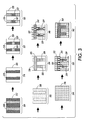
- Figure 3 shows a top view of the TFT at various stages of the process described in Figure 2.
- a transparent substrate is coated with a layer of a transparent conductor such as ITO.
- An opaque conductor typically an opaque metal such as chrome is deposited over the transparent conductor in block 208.
- the opaque conductor and transparent conductors are subsequently patterned to create features that aid in the fabrication and also to control the operation of the TFTs.
- the conductors are deposited via jet printing avoiding the need for subsequent patterning.
- the printing is done using wax resists as described in blocks 212 and 216.
- a wax resist is printed to define the opaque metal as a mask for the gate lines to couple a power source to the TFT.
- Structure 304 of Figure 3 shows a printed wax region 308 defining the mask for the gate lines in opaque conductor 312.
- the opaque conductor is etched. The wax acts as a mask resulting in a gate line made of an opaque conductor. The wax mask is removed in block 220.
- the transparent conductor is then etched in block 222.
- the etched opaque conductor acts as a etch mask for the transparent conductor.
- Structure 316 of Figure 3 illustrates the resulting opaque conductor on transparent conductor region 318 on top of transparent substrate layer 320.
- Block 224 describes a printing of a wax mask that defines a gate pad.
- Structure 322 shows deposition of wax mask 324 over the line consisting of the opaque metal on the transparent conductor 320.
- the opaque conductor is etched in block 228.
- the wax mask protects the region under the mask such that removal of the wax mask in block 232 results in the opaque gate pad shown in structure 325.
- transparent conductor lines 326 couple chrome gate pads 327 to a controlling circuit (not shown).
- the procedure by which a wax is deposited, the conductor is etched, and the wax is removed is well known in the art. A detailed description is provided in US Patent application serial number 09/838,684 and 09/838,685, both filed April 14, 2001 (attorney dockets A1205 and A1205Q) which are hereby incorporated by reference.
- Blocks 236 to 252 of Figure 2 describe the formation of the source and drain of a TFT structure.
- a thin dielectric film 330 such as a silicon dioxide or a polymer is deposited on a substrate as shown in structure 332.
- a second opaque conductor layer is deposited on the substrate. The second opaque conductor layer is patterned to form the source and drain contacts and the data lines.
- a wax mask is deposited in block 244. The wax mask protects regions of the conductor that will be used to form source pads, drain pads and data lines.
- Structure 334 of figure 3 shows the wax pattern on opaque conductor 335. The wax pattern masks data line 336 and source and drain pads 338.
- the conductor is etched in block 248 forming the data line and drain pads.
- the wax is removed leaving structure 340.
- the resulting opaque conductor pattern forms source and drain contacts 339 as well as common data lines 342 connecting the TFTs in the TFT array.
- Blocks 256 to 280 describe the formation of the semiconductor layer of the TFT.
- a photosensitive polymer 346 typically SU-8 or other optically definable material, is deposited over the substrate as shown in structure 344. Deposition methods used to deposit the photosensitive polymer may include spin or dip coating.
- a radiation source provides radiation that defines the unmasked regions of the photosensitive polymer. In one embodiment of the invention, the radiation exposure occurs through a backside of the substrate such that the opaque conductors between the substrate and the photosensitive polymer serve as a mask blocking the patterning radiation.
- the mask includes the gate pads, the source and drain and the data line regions.
- Structure 350 of Figure 3 shows the resulting structure where the exposed regions of polymer 352 define a network of openings.
- the network includes channels covering data lines 342 and covering the source-drain-gate pad regions 327, 339 of the TFTs in an array of TFTs.
- a solution of a TFT active material fills the network of openings in block 268.
- the solution is usually an organic semiconductor such as a poly(thiophene)-based polymer or poly(9-9'-dioctylfluorene-co-bithiophene).
- Other solution processable organic semiconductors such as thermally-curable, soluble precursors to pentacene may also be used.
- the fluidic channels connect the series of openings and distribute the organic semiconductor throughout the circuit.
- the distribution system allows the fluid source to remain stationary and to deposit the fluid at one point of the channel. If faster filling speeds or large areas are required, the fluid source or a plurality of fluid sources could be moved to several positions along a microchannel. In the illustrated case, the number of distribution points for filling the microchannels is much smaller than the number of electronic devices or TFTs being formed along the microchannel, thus to at least one of the electronic devices, the microchannel is the primary source of semiconductor material.
- Structure 362 of Figure 3 shows the fluidic channels filled with organic semiconductor 364.
- Using microchannels to distribute semiconductor material allows the use of semiconductor materials that are difficult to jet print due to limited solubility or material incompatibilities with common printheads.
- the fluidic semiconductor is allowed to dry in block 272.
- the fluidic semiconductor typically includes a carrier solution and a semiconductor material disolved in the carrier solution. As the carrier solution evaporates, a residue remains and serves as semiconductor solid that forms part of the TFT.
- a protective polymer such as poly(methylmethacrylate), poly(vinylalcohol), or poly(styrene) can be deposited into the fluidic channels in block 276.
- the protective polymer can be dissolved in a solvent and allowed to flow through the network of channels.
- the dried film encapsulates the semiconductor layer of block 272.
- each channel includes a bottom portion filled with semiconductor and a top portion filled with a protective polymer.
- the substrate is planarized.
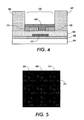
- Figure 4 shows a cross sectional side view of an example TFT created using the methods of Figure 2 and 3.
- transparent substrate 404 supports a TFT structure.
- a conducting gate line 408 carries electrical signals to control a gate pad 412.
- the gate is separated from the source 416 and drain 420 by a thin dielectric layer 424 which prevents electrical shorting of gate 412 with source 416 and drain 420.
- Channel walls 428, 432 define a channel 436.
- a portion of the channel cavity includes the region between source 416 and drain 420.
- a semiconductor material 440 which, at one point in time, was dissolved or suspended in a solvent carrier fills in the region between source 416 and drain 420.
- the channel walls confine the solvent and semiconductor material 440 until the solvent evaporates and the semiconductor material dries.
- FIG. 5 shows a top view of an array of TFTs coupled by microchannels that were used to distribute the solution-processable semiconductor.
- Each TFT semiconductor region 504, 508, 512 which includes the semiconductor over a source-gate-drain region, is coupled to other TFT semiconductor regions via corresponding microchannels 516.
- the microchannel was formed using the data line that addresses each source pad as a mask, in the example provided, usually two TFTs.
- a channel is defined as a region between two walls that is appropriate for confining a fluid, but allows a fluid to flow in a direction approximately parallel to a surface of the wall.
- the channel has a much longer length than width.
- the channel connects at least two circuit elements.
Landscapes
- Engineering & Computer Science (AREA)
- Manufacturing & Machinery (AREA)
- Thin Film Transistor (AREA)
- Bipolar Transistors (AREA)
- Exposure And Positioning Against Photoresist Photosensitive Materials (AREA)
- Electroluminescent Light Sources (AREA)
- Liquid Deposition Of Substances Of Which Semiconductor Devices Are Composed (AREA)
Abstract
Description
- The invention relates to semiconductor processing, more particularly, the invention relates to the fabrication of large-area arrays of thin film transistors.
- In recent years, large area thin-film transistor (TFT) arrays have found important applications in imaging devices and display devices. However, fabrication of arrays of TFTs is relatively expensive due in part to the cost and complexity of the photolithographically-based processing techniques used in the fabrication process.
- Recently organic semiconductors have been used to form TFT arrays. Such organic semiconductors are preferred due to their compatibility with flexible substrates. Using organic semiconductors also reduces fabrication costs. One reason for the lower fabrication costs is that solution -processable organic semiconductors can be patterned using jet-printing, screen printing, or micromolding. Jet printing is described in U.S. patent 5,972,419 "Electroluminescent Display and Method for Making the Same", WO0146987A2 "Inkjet-Fabricated Integrated Circuits"; screen printing is described in "All-Polymer Field Effect Transistor Realized by Printing Techniques" F. Garnier, R. Hajlaoui, A. Yassar, P. Srivastava Science 265 1994 p1684-1686 and micromolding is described in U.S. patent 6,322,736 "Method for Fabricating Molded Microstructures on Substrates".
- However jet printing, micromolding and screen printing-based fabrication processes are not without difficulties. Jet-printing of organic semiconductors is a serial process and is thus slow. Also, jet printing of organic semiconductors is difficult because such printing involves special printheads maintained in precise alignment with printed features for extended periods of time. In addition, the size of the printed features is controlled, in part, by the wettability of the jetted solution on the substrate. Wettablility can be difficult to precisely control.
- Micromolding techniques also present difficulties. Molding techniques usually call for the mold, frequently formed from an elastomeric polymer, be brought into contact with a substrate over a large area. Good registration of the mold and substrate can be difficult to achieve. Often, elastomeric molds are incompatible with the organic solvents used to dissolve the organic semiconductors. Screen printing is faster than jet printing because screen printing provides a parallel method of depositing the organic semiconductor. However, screen printing is typically incapable of fabricating small features with dimensions less than 100 micrometers due to: spreading of the deposited liquid on the substrate, difficulties in fabricating screens with fine features, and difficulties in registration between the screen and previously patterned features.
- Thus a method of patterning small feature sizes with a solution-based organic semiconductor in a rapid, highly parallel manner is needed.
- An improved method of semiconductor processing is described. In the method, a series of micro-channels are formed to interconnect a plurality of electronic devices being formed. A solution including a solution-processable semiconductor flows into the microfluidic channels and is allowed to dry. Thus, the microchannel distributes the solution and the residue remaining after the solvent evaporates forms a part of the electronic device being formed.
- In one embodiment of the method as defined in claim 1, the solution comprises an organic polymeric semiconductor.
- In a further embodiment the solution comprises a colloidal suspension of an inorganic semiconductor.
- In a further embodiment the solution comprises an organic molecular semiconductor.
- In a further embodiment the residue is a semiconductor.
- In a further embodiment the opaque lines are lines coupling source to drain regions of thin film transistors in an array of thin film transistors.
- In one embodiment of the method as defined in claim 10, the method further comprises the operation of:
- patterning conducting gates of a plurality of thin film transistors coupled to the opaque lines.
-
- In a further embodiment the method further comprises the operation of:
- patterning opaque source and drain conductors in a second conductor layer over the conducting gates.
-
- In a further embodiment the method further comprises the operation of:
- distributing a solution containing a semiconductor to the plurality of thin film transistors via microfluidic channels.
-
- In a further embodiment the method further comprises the operation of:
- patterning conducting drains of a plurality of thin film transistors coupled to the opaque lines.
-
- In a further embodiment the method further comprises the operation of:
- patterning conducting sources of a plurality of thin film transistors coupled to the opaque lines.
-
- In a further embodiment the microchannels have a width of less than 500 microns.
- According to another aspect of the present invention a method of forming an array of thin film transistors comprises:
- forming a source-gate-drain region of each thin film transistor in a plurality of thin film transistors;
- forming a conducting line from an opaque conductor that couples to the source-gate-drain region of each thin film transistor in the plurality of thin film transistors;
- forming a microchannel from a photosensitive polymer, the microchannel self aligned with the conducting line made from the opaque conductor.
-
- In a further embodiment the method further comprises the operation of distributing a fluidic semiconductor through the microchannel to form each thin film transistor in the array of thin film transistors.
-
- Figure 1 shows a schematic of the process flow for fabricating self aligned microfluidic channels in one embodiment of the invention.
- Figure 2 is a flow chart that describes the process of forming a TFT using microfluidic channels.
- Figure 3 is a top level view of a TFT being fabricated at various stages in the flow chart of Figure 2.
- Figure 4 shows a side cross sectional view of a microfluidic channel and the associated TFT.
- Figure 5 shows a resulting TFT array fabricated using the process flows described in Figures 1 through 3.
-
- A system of forming a self-aligned microfluidic channel is described. The system is particularly well suited to fabricating fluidic channels that interconnect TFTs in an array of TFTs.
- Figure 1 provides a schematic of the process flow for fabrication of self-aligned microfluidic channels for TFTs. In
section 104 of the process flow, afirst surface 106 oftransparent substrate 108 is patterned with anopaque pattern 112. The transparent substrate may be made from a variety of materials such as glass or plastic that passes most of the light in the ultraviolet or visible spectrum without significant attenuation; usually more than 50 percent of the light will pass through the substrate. - One method of simplifying the TFT fabrication process is to self-align the organic semiconductor used in TFT formation with the electrodes that will control the gate of the TFT and the electrodes that will control the source-drain voltage of the TFT. The conductive lines that form the data interconnects between the source regions of the TFTs can also be coated with the semiconductor without adversely affecting the performance of the TFTs. One method of accomplishing self-alignment is to fabricate the source, drain, and gate pad electrodes and data interconnect lines with an opaque conductor and subsequently to use the opaque conductor as a photomask. Thus, in one embodiment of the invention, at least a part of
opaque pattern 112 is made from conducting lines, typically a metal such as gold or chrome. The metal forms the electrodes that control current flow in the source and drain regions, the gate pad that controls the gate voltage, and the interconnect lines connecting the source electrodes. The metal may be patterned using a variety of techniques, including but not limited to, wax-resist printing. - Not every conductor used in a TFT array is associated with a corresponding organic semiconductor region. Thus, in one embodiment of the invention, a second pattern of
conductors 116 is formed using a transparent conductor, typically indium-tin oxide (ITO). The ITO forms the conducting parts of the TFT array control circuitry that are not associated with any organic semiconductor regions. - In
section 120 of Figure 1, afirst surface 106 oftransparent substrate 108 and an associated opaque and transparent pattern ofconductors polymer 124. The polymer is typically a photosensitive polymer such as SU-8, a commercially available type of optically curable epoxy, or other photosensitive material. The polymer may be coated onsubstrate 108 using a variety of techniques such as spin coating or dip coating. - In order to pattern the photosensitive material,
section 130 of Figure 1 shows light 134 passing throughtransparent substrate 108. Light passing throughtransparent substrate 108 develops exposed portions of the polymer. The light is typically UV or visible light having a wavelength between 200 and 600 nm. The light can define the photosensitive polymer by cross-linking functional groups in the polymer material or by creating functional groups that cross-link when heated. Thus, these processes change the physical properties of the polymer in the exposed region. Regions masked by theopaque conductor pattern 112 are not exposed to light of the particular frequency range and remain undeveloped. The undeveloped polymer is easily removed by stripping with a solvent. -
Section 140 of Figure 1 shows the resulting structure after the uncured polymer is removed. As illustrated, removal of the undeveloped polymer results in the formation offluidic channels 144. The dimensions of each fluidic channel depend on the width of the original masking opaque conductor, the exposure characteristics of the photosensitive polymer, and the wavelength of light used in the curing process. The width of each fluidic channel may be smaller than can be formed using other techniques. Typically, each channel is significantly less than 500 micrometers in width, more usually less than 200 micrometers in width. When short wavelengths are used for photodevelopment, the width of the channel may be reduced to a size on the order of 0.5 micrometers. -
Section 150 of Figure 1 shows the deposition of a solution containing a semiconductor, typically a solution-processable organic semiconductor, into the channels. The solution-processable semiconductor is typically an organic polymer that is dissolved in a solvent that has a low viscosity, typically below 50 cP(measure of viscosity). Suspensions of colloidal or nanoparticulate inorganic semiconductors in solution form can also be used. Deposition of the solution-processable semiconductor may occur at one position in the microfluidic network. After deposition, the low viscosity allows the fluid containing the semiconductor to redistribute throughout the microfluidic network via natural capillary flow such that after a short amount of time, the fluid levels in the various interconnected microchannels are approximately equal. Deposition of the solution containing the semiconductor may be done using a variety of techniques, including micropipetting, piezo-based dispensing, and simple capillary action. Insection 150, asyringe 154 and needle or micro-pipet structure is shown being used to deposit the solution containing the solution processable semiconductor. - After distributing the solution-processable semiconductor throughout the microchannels, the solution is allowed to dry in a low-particulate count environment to minimize the chances of contamination. In one embodiment, a heat source is used to control the drying process. The dried film or residue from the semiconductor solution produces a semiconductor layer of the TFT.
- The described process is particularly well suited for fabricating a TFT structure, although it may be used to form other structures. Figure 2 provides a flow chart describing one method of using microfluidic channels to form a TFT array. Figure 3 shows a top view of the TFT at various stages of the process described in Figure 2.
- In
block 204 of Figure 2, a transparent substrate is coated with a layer of a transparent conductor such as ITO. An opaque conductor, typically an opaque metal such as chrome is deposited over the transparent conductor inblock 208. The opaque conductor and transparent conductors are subsequently patterned to create features that aid in the fabrication and also to control the operation of the TFTs. - A number of methods may be used to pattern the conductors. In one embodiment, the conductors are deposited via jet printing avoiding the need for subsequent patterning. In another embodiment, the printing is done using wax resists as described in
blocks block 212, a wax resist is printed to define the opaque metal as a mask for the gate lines to couple a power source to the TFT.Structure 304 of Figure 3 shows a printedwax region 308 defining the mask for the gate lines inopaque conductor 312. Inblock 216 of Figure 2, the opaque conductor is etched. The wax acts as a mask resulting in a gate line made of an opaque conductor. The wax mask is removed inblock 220. The transparent conductor is then etched inblock 222. The etched opaque conductor acts as a etch mask for the transparent conductor.Structure 316 of Figure 3 illustrates the resulting opaque conductor ontransparent conductor region 318 on top oftransparent substrate layer 320. - Next, the opaque gate pads are formed.
Block 224 describes a printing of a wax mask that defines a gate pad.Structure 322 shows deposition ofwax mask 324 over the line consisting of the opaque metal on thetransparent conductor 320. The opaque conductor is etched inblock 228. The wax mask protects the region under the mask such that removal of the wax mask inblock 232 results in the opaque gate pad shown instructure 325. Instructure 325, transparent conductor lines 326 couplechrome gate pads 327 to a controlling circuit (not shown). The procedure by which a wax is deposited, the conductor is etched, and the wax is removed is well known in the art. A detailed description is provided in US Patent application serial number 09/838,684 and 09/838,685, both filed April 14, 2001 (attorney dockets A1205 and A1205Q) which are hereby incorporated by reference. -
Blocks 236 to 252 of Figure 2 describe the formation of the source and drain of a TFT structure. Inblock 236, athin dielectric film 330, such as a silicon dioxide or a polymer is deposited on a substrate as shown instructure 332. Inblock 240 of figure 2, a second opaque conductor layer is deposited on the substrate. The second opaque conductor layer is patterned to form the source and drain contacts and the data lines. In one patterning method, a wax mask is deposited inblock 244. The wax mask protects regions of the conductor that will be used to form source pads, drain pads and data lines.Structure 334 of figure 3 shows the wax pattern onopaque conductor 335. The wax pattern masksdata line 336 and source and drainpads 338. The conductor is etched inblock 248 forming the data line and drain pads. Inblock 252, the wax is removed leavingstructure 340. The resulting opaque conductor pattern forms source anddrain contacts 339 as well ascommon data lines 342 connecting the TFTs in the TFT array. -
Blocks 256 to 280 describe the formation of the semiconductor layer of the TFT. In block 256 aphotosensitive polymer 346, typically SU-8 or other optically definable material, is deposited over the substrate as shown instructure 344. Deposition methods used to deposit the photosensitive polymer may include spin or dip coating. Inblock 260, a radiation source provides radiation that defines the unmasked regions of the photosensitive polymer. In one embodiment of the invention, the radiation exposure occurs through a backside of the substrate such that the opaque conductors between the substrate and the photosensitive polymer serve as a mask blocking the patterning radiation. When forming a TFT, using microchannels, the mask includes the gate pads, the source and drain and the data line regions. - In
block 264, unexposed regions of the photosensitive polymer are removed using a solvent.Structure 350 of Figure 3 shows the resulting structure where the exposed regions ofpolymer 352 define a network of openings. The network includes channels coveringdata lines 342 and covering the source-drain-gate pad regions block 268. The solution is usually an organic semiconductor such as a poly(thiophene)-based polymer or poly(9-9'-dioctylfluorene-co-bithiophene). Other solution processable organic semiconductors such as thermally-curable, soluble precursors to pentacene may also be used. - The fluidic channels connect the series of openings and distribute the organic semiconductor throughout the circuit. The distribution system allows the fluid source to remain stationary and to deposit the fluid at one point of the channel. If faster filling speeds or large areas are required, the fluid source or a plurality of fluid sources could be moved to several positions along a microchannel. In the illustrated case, the number of distribution points for filling the microchannels is much smaller than the number of electronic devices or TFTs being formed along the microchannel, thus to at least one of the electronic devices, the microchannel is the primary source of semiconductor material.
-
Structure 362 of Figure 3 shows the fluidic channels filled withorganic semiconductor 364. Using microchannels to distribute semiconductor material allows the use of semiconductor materials that are difficult to jet print due to limited solubility or material incompatibilities with common printheads. The fluidic semiconductor is allowed to dry inblock 272. The fluidic semiconductor typically includes a carrier solution and a semiconductor material disolved in the carrier solution. As the carrier solution evaporates, a residue remains and serves as semiconductor solid that forms part of the TFT. - In order to protect the semiconductor, a protective polymer such as poly(methylmethacrylate), poly(vinylalcohol), or poly(styrene) can be deposited into the fluidic channels in
block 276. The protective polymer can be dissolved in a solvent and allowed to flow through the network of channels. The dried film encapsulates the semiconductor layer ofblock 272. Thus each channel includes a bottom portion filled with semiconductor and a top portion filled with a protective polymer. Inblock 280, the substrate is planarized. - Figure 4 shows a cross sectional side view of an example TFT created using the methods of Figure 2 and 3. In Figure 4,
transparent substrate 404 supports a TFT structure. A conductinggate line 408 carries electrical signals to control agate pad 412. The gate is separated from thesource 416 and drain 420 by athin dielectric layer 424 which prevents electrical shorting ofgate 412 withsource 416 and drain 420. -
Channel walls channel 436. A portion of the channel cavity includes the region betweensource 416 and drain 420. Asemiconductor material 440 which, at one point in time, was dissolved or suspended in a solvent carrier fills in the region betweensource 416 and drain 420. The channel walls confine the solvent andsemiconductor material 440 until the solvent evaporates and the semiconductor material dries. - Figure 5 shows a top view of an array of TFTs coupled by microchannels that were used to distribute the solution-processable semiconductor. Each
TFT semiconductor region microchannels 516. The microchannel was formed using the data line that addresses each source pad as a mask, in the example provided, usually two TFTs. - As used herein, a channel is defined as a region between two walls that is appropriate for confining a fluid, but allows a fluid to flow in a direction approximately parallel to a surface of the wall. The channel has a much longer length than width. When used in a circuit, the channel connects at least two circuit elements.
- The preceding description has described in detail using microfluidic channels to distribute a solution-processable semiconductor to form arrays of semiconductor devices. In order to improve the readers understanding of the device, the detailed description includes a number of details such as the type of device (a TFT) being formed, and the type of fluidic semiconductor. Such details are included to facilitate understanding of the invention and should not be interpreted to restrict the scope of the invention. For example, instead of TFTs, the preceding description may be used to form other semiconductor devices such as light emitting diodes. Thus, the scope of the invention should only be limited by the claims set forth below.
Claims (10)
- A method of forming a plurality of electronic devices comprising the operations of:patterning at least two electrical contacts, each electrical contact corresponding to a device in a plurality of electronic devices on a substrate;forming a microfluidic channel interconnecting the electrical contacts to deliver a solution to the at least two electrical contacts formed on the substrate;delivering a solution through the microfluidic channel; andallowing the solution to dry leaving a residue that forms a part of each device in the plurality of electronic devices.
- The method of claim 1 wherein each electronic device is a thin film transistor
- The method of claim 1 wherein the microfluidic channel couples together electrodes used to form a plurality of thin film transistors in an array of thin film transistors.
- The method of claim 1 wherein the microfluidic channels couple together electrodes used to form a plurality of light emitting diodes.
- The method of claim 1 wherein the operation of forming the microfluidic channels includes a process of patterning a photosensitive polymer through a photomask.
- The method of claim 5 wherein the substrate is transparent and the electrodes are formed from an opaque material, the electrode used as a photomask for patterning the photosensitive polymer.
- The method of claim 6 further comprising the operation of:using an opaque line coupling the electrodes as part of the photomask for patterning the photosensitive polymer, the uncured portion of the photosensitive polymer corresponding to the line forming said microfluidic channel.
- The method of claim 1 further comprising the operation of:flowing a protective polymer through the microchannels, the protective polymer to protect the residue.
- The method of claim 5 wherein the photosensitive polymer is SU-8.
- A method of forming a plurality of semiconductor devices comprising the operations of:patterning opaque lines on a first side of a transparent substrate;depositing a photosensitive polymer over the opaque lines; and,using the opaque lines as a photomask to form microfluidic channels.
Applications Claiming Priority (2)
| Application Number | Priority Date | Filing Date | Title |
|---|---|---|---|
| US10/303,551 US6872588B2 (en) | 2002-11-22 | 2002-11-22 | Method of fabrication of electronic devices using microfluidic channels |
| US303551 | 2002-11-22 |
Publications (3)
| Publication Number | Publication Date |
|---|---|
| EP1422766A2 true EP1422766A2 (en) | 2004-05-26 |
| EP1422766A3 EP1422766A3 (en) | 2007-06-06 |
| EP1422766B1 EP1422766B1 (en) | 2011-01-19 |
Family
ID=32229935
Family Applications (1)
| Application Number | Title | Priority Date | Filing Date |
|---|---|---|---|
| EP03026733A Expired - Lifetime EP1422766B1 (en) | 2002-11-22 | 2003-11-21 | Method of fabrication of electronic devices using microfluidic channels |
Country Status (6)
| Country | Link |
|---|---|
| US (1) | US6872588B2 (en) |
| EP (1) | EP1422766B1 (en) |
| JP (1) | JP4699687B2 (en) |
| BR (1) | BR0305303A (en) |
| CA (1) | CA2449632C (en) |
| DE (1) | DE60335772D1 (en) |
Cited By (10)
| Publication number | Priority date | Publication date | Assignee | Title |
|---|---|---|---|---|
| EP1703573A1 (en) * | 2005-03-19 | 2006-09-20 | Samsung SDI Co., Ltd. | Organic thin film transistor, flat display device including the same, and method of manufacturing the organic thin film transistor |
| WO2006120414A3 (en) * | 2005-05-09 | 2007-05-03 | Univ Manchester | Electronic devices |
| WO2009075650A1 (en) * | 2007-12-11 | 2009-06-18 | Nanyang Polytechnic | A method of doping and apparatus for doping |
| WO2010042170A3 (en) * | 2008-10-09 | 2010-06-03 | Eastman Kodak Company | Interconnection of adjacent devices |
| CN101283461B (en) * | 2005-05-09 | 2012-04-04 | 纳米电子印刷有限公司 | Electronic devices |
| WO2013065276A1 (en) * | 2011-11-04 | 2013-05-10 | Sony Corporation | Organic single crystal film, organic single crystal film array, and semiconductor device including an organic single crystal film |
| EP2122690A4 (en) * | 2007-02-15 | 2013-08-21 | Massachusetts Inst Technology | SOLAR CELLS HAVING TEXTURED SURFACES |
| CN105116038A (en) * | 2015-07-20 | 2015-12-02 | 深圳大学 | Organic semiconductor based immunodetection integrated chip and preparation method thereof |
| CN107046097A (en) * | 2017-05-11 | 2017-08-15 | 京东方科技集团股份有限公司 | Display panel manufacture method, the manufacturing equipment of display panel and display panel |
| WO2019066912A1 (en) * | 2017-09-29 | 2019-04-04 | Intel Corporation | Self-aligned contacts for thin film transistors |
Families Citing this family (20)
| Publication number | Priority date | Publication date | Assignee | Title |
|---|---|---|---|---|
| US7087444B2 (en) * | 2002-12-16 | 2006-08-08 | Palo Alto Research Center Incorporated | Method for integration of microelectronic components with microfluidic devices |
| KR100669802B1 (en) * | 2004-12-04 | 2007-01-16 | 삼성에스디아이 주식회사 | A thin film transistor, a method of manufacturing the same, and a flat panel display device having the thin film transistor |
| TWI254027B (en) * | 2004-12-07 | 2006-05-01 | Ind Tech Res Inst | Micro device and manufacturing method thereof |
| KR20070009013A (en) * | 2005-07-14 | 2007-01-18 | 삼성전자주식회사 | Flat panel display and flat panel display manufacturing method |
| US7498119B2 (en) * | 2006-01-20 | 2009-03-03 | Palo Alto Research Center Incorporated | Process for forming a feature by undercutting a printed mask |
| US7365022B2 (en) * | 2006-01-20 | 2008-04-29 | Palo Alto Research Center Incorporated | Additive printed mask process and structures produced thereby |
| US7384568B2 (en) * | 2006-03-31 | 2008-06-10 | Palo Alto Research Center Incorporated | Method of forming a darkfield etch mask |
| US9164037B2 (en) * | 2007-01-26 | 2015-10-20 | Palo Alto Research Center Incorporated | Method and system for evaluation of signals received from spatially modulated excitation and emission to accurately determine particle positions and distances |
| US8821799B2 (en) * | 2007-01-26 | 2014-09-02 | Palo Alto Research Center Incorporated | Method and system implementing spatially modulated excitation or emission for particle characterization with enhanced sensitivity |
| WO2008119066A1 (en) * | 2007-03-28 | 2008-10-02 | The Regents Of The University Of California | Single-sided lateral-field and phototransistor-based optoelectronic tweezers |
| US8551556B2 (en) * | 2007-11-20 | 2013-10-08 | Palo Alto Research Center Incorporated | Method for obtaining controlled sidewall profile in print-patterned structures |
| WO2009066235A1 (en) * | 2007-11-22 | 2009-05-28 | Koninklijke Philips Electronics N.V. | Combined optical and electrical sensor cartridges |
| US8629981B2 (en) | 2008-02-01 | 2014-01-14 | Palo Alto Research Center Incorporated | Analyzers with time variation based on color-coded spatial modulation |
| US8373860B2 (en) | 2008-02-01 | 2013-02-12 | Palo Alto Research Center Incorporated | Transmitting/reflecting emanating light with time variation |
| WO2009145857A1 (en) * | 2008-04-18 | 2009-12-03 | 1366 Technologies Inc. | Methods to pattern diffusion layers in solar cells and solar cells made by such methods |
| US8136922B2 (en) * | 2009-09-01 | 2012-03-20 | Xerox Corporation | Self-assembly monolayer modified printhead |
| US8679984B2 (en) | 2011-06-30 | 2014-03-25 | Samsung Electronics Co., Ltd. | Method of manufacturing electric device, array of electric devices, and manufacturing method therefor |
| US9029800B2 (en) | 2011-08-09 | 2015-05-12 | Palo Alto Research Center Incorporated | Compact analyzer with spatial modulation and multiple intensity modulated excitation sources |
| US8723140B2 (en) | 2011-08-09 | 2014-05-13 | Palo Alto Research Center Incorporated | Particle analyzer with spatial modulation and long lifetime bioprobes |
| CN112255666B (en) * | 2020-10-23 | 2022-11-18 | 中国工程物理研究院激光聚变研究中心 | Neutron sensitive microchannel plate |
Citations (2)
| Publication number | Priority date | Publication date | Assignee | Title |
|---|---|---|---|---|
| WO2001095384A1 (en) | 2000-06-03 | 2001-12-13 | The University Of Liverpool | A method of electronic component fabrication and an electronic component |
| WO2002082560A1 (en) | 2001-04-04 | 2002-10-17 | Infineon Technologies Ag | Self-aligned contact doping for organic field effect transistors |
Family Cites Families (28)
| Publication number | Priority date | Publication date | Assignee | Title |
|---|---|---|---|---|
| DE3856483T2 (en) * | 1987-03-18 | 2002-04-18 | Kabushiki Kaisha Toshiba, Kawasaki | Process for the production of thin layers |
| JPH03145767A (en) * | 1989-10-31 | 1991-06-20 | Fujitsu Ltd | Manufacture of thin film transistor |
| US5699157A (en) * | 1996-07-16 | 1997-12-16 | Caliper Technologies Corp. | Fourier detection of species migrating in a microchannel |
| US6136212A (en) * | 1996-08-12 | 2000-10-24 | The Regents Of The University Of Michigan | Polymer-based micromachining for microfluidic devices |
| US6152071A (en) * | 1996-12-11 | 2000-11-28 | Canon Kabushiki Kaisha | High-frequency introducing means, plasma treatment apparatus, and plasma treatment method |
| JPH10256558A (en) * | 1997-03-17 | 1998-09-25 | Toshiba Corp | Method of manufacturing thin film transistor array, electronic device, and thin film transistor |
| US6669803B1 (en) * | 1997-10-03 | 2003-12-30 | Digital Optics Corp. | Simultaneous provision of controlled height bonding material at a wafer level and associated structures |
| US6685809B1 (en) * | 1999-02-04 | 2004-02-03 | Ut-Battelle, Llc | Methods for forming small-volume electrical contacts and material manipulations with fluidic microchannels |
| US6033202A (en) | 1998-03-27 | 2000-03-07 | Lucent Technologies Inc. | Mold for non - photolithographic fabrication of microstructures |
| US6159871A (en) * | 1998-05-29 | 2000-12-12 | Dow Corning Corporation | Method for producing hydrogenated silicon oxycarbide films having low dielectric constant |
| KR100308851B1 (en) * | 1998-11-04 | 2001-12-17 | 구본준, 론 위라하디락사 | Method of forming insulating film pattern of liquid crystal display device |
| US6247986B1 (en) * | 1998-12-23 | 2001-06-19 | 3M Innovative Properties Company | Method for precise molding and alignment of structures on a substrate using a stretchable mold |
| JP2000269504A (en) * | 1999-03-16 | 2000-09-29 | Hitachi Ltd | Semiconductor device, manufacturing method thereof, and liquid crystal display device |
| JP3084367B1 (en) * | 1999-03-17 | 2000-09-04 | キヤノン販売株式会社 | Method of forming interlayer insulating film and semiconductor device |
| US6225238B1 (en) * | 1999-06-07 | 2001-05-01 | Allied Signal Inc | Low dielectric constant polyorganosilicon coatings generated from polycarbosilanes |
| JP2001244467A (en) * | 2000-02-28 | 2001-09-07 | Hitachi Ltd | Coplanar semiconductor device, display device and manufacturing method using the same |
| TW531802B (en) * | 2000-07-21 | 2003-05-11 | Canon Sales Co Ltd | Semiconductor device and semiconductor device manufacturing method |
| US6448186B1 (en) * | 2000-10-06 | 2002-09-10 | Novellus Systems, Inc. | Method and apparatus for use of hydrogen and silanes in plasma |
| US6537923B1 (en) * | 2000-10-31 | 2003-03-25 | Lsi Logic Corporation | Process for forming integrated circuit structure with low dielectric constant material between closely spaced apart metal lines |
| US6582890B2 (en) * | 2001-03-05 | 2003-06-24 | Sandia Corporation | Multiple wavelength photolithography for preparing multilayer microstructures |
| US6627111B2 (en) * | 2001-03-06 | 2003-09-30 | International Business Machines Corp. | Organic light emitting displays and new fluorescent compounds |
| US6472333B2 (en) * | 2001-03-28 | 2002-10-29 | Applied Materials, Inc. | Silicon carbide cap layers for low dielectric constant silicon oxide layers |
| US6452207B1 (en) * | 2001-03-30 | 2002-09-17 | Lucent Technologies Inc. | Organic semiconductor devices |
| JP4841751B2 (en) * | 2001-06-01 | 2011-12-21 | 株式会社半導体エネルギー研究所 | Organic semiconductor device and manufacturing method thereof |
| US6669454B2 (en) * | 2001-06-05 | 2003-12-30 | Wisconsin Alumni Research Foundation | Microfluidic actuation method and apparatus |
| US6634732B2 (en) * | 2001-09-11 | 2003-10-21 | Hewlett-Packard Development Company, L.P. | Thermoplastic polymer film sealing of nozzles on fluid ejection devices and method |
| US6698868B2 (en) * | 2001-10-31 | 2004-03-02 | Hewlett-Packard Development Company, L.P. | Thermal drop generator for ultra-small droplets |
| US6778718B2 (en) * | 2001-11-09 | 2004-08-17 | Corning Incorporated | Alignment of active optical components with waveguides |
-
2002
- 2002-11-22 US US10/303,551 patent/US6872588B2/en not_active Expired - Fee Related
-
2003
- 2003-11-17 CA CA002449632A patent/CA2449632C/en not_active Expired - Fee Related
- 2003-11-20 JP JP2003390153A patent/JP4699687B2/en not_active Expired - Fee Related
- 2003-11-21 BR BR0305303-2A patent/BR0305303A/en active Search and Examination
- 2003-11-21 DE DE60335772T patent/DE60335772D1/en not_active Expired - Lifetime
- 2003-11-21 EP EP03026733A patent/EP1422766B1/en not_active Expired - Lifetime
Patent Citations (2)
| Publication number | Priority date | Publication date | Assignee | Title |
|---|---|---|---|---|
| WO2001095384A1 (en) | 2000-06-03 | 2001-12-13 | The University Of Liverpool | A method of electronic component fabrication and an electronic component |
| WO2002082560A1 (en) | 2001-04-04 | 2002-10-17 | Infineon Technologies Ag | Self-aligned contact doping for organic field effect transistors |
Cited By (15)
| Publication number | Priority date | Publication date | Assignee | Title |
|---|---|---|---|---|
| US7714321B2 (en) | 2005-03-19 | 2010-05-11 | Samsung Mobile Display Co., Ltd. | Organic thin film transistor, flat display device including the same, and method of manufacturing the organic thin film transistor |
| EP1703573A1 (en) * | 2005-03-19 | 2006-09-20 | Samsung SDI Co., Ltd. | Organic thin film transistor, flat display device including the same, and method of manufacturing the organic thin film transistor |
| US9076851B2 (en) | 2005-05-09 | 2015-07-07 | Pragmatic Printing Limited | Planar electronic semiconductor device |
| CN101283461B (en) * | 2005-05-09 | 2012-04-04 | 纳米电子印刷有限公司 | Electronic devices |
| US8624216B2 (en) | 2005-05-09 | 2014-01-07 | Pragmatic Printing Limited | Planar electronic semiconductor device |
| WO2006120414A3 (en) * | 2005-05-09 | 2007-05-03 | Univ Manchester | Electronic devices |
| EP2122690A4 (en) * | 2007-02-15 | 2013-08-21 | Massachusetts Inst Technology | SOLAR CELLS HAVING TEXTURED SURFACES |
| WO2009075650A1 (en) * | 2007-12-11 | 2009-06-18 | Nanyang Polytechnic | A method of doping and apparatus for doping |
| WO2010042170A3 (en) * | 2008-10-09 | 2010-06-03 | Eastman Kodak Company | Interconnection of adjacent devices |
| WO2013065276A1 (en) * | 2011-11-04 | 2013-05-10 | Sony Corporation | Organic single crystal film, organic single crystal film array, and semiconductor device including an organic single crystal film |
| CN105116038A (en) * | 2015-07-20 | 2015-12-02 | 深圳大学 | Organic semiconductor based immunodetection integrated chip and preparation method thereof |
| CN105116038B (en) * | 2015-07-20 | 2018-06-29 | 深圳大学 | One kind is based on organic semi-conductor immune detection integrated chip and preparation method thereof |
| CN107046097A (en) * | 2017-05-11 | 2017-08-15 | 京东方科技集团股份有限公司 | Display panel manufacture method, the manufacturing equipment of display panel and display panel |
| WO2019066912A1 (en) * | 2017-09-29 | 2019-04-04 | Intel Corporation | Self-aligned contacts for thin film transistors |
| US12183831B2 (en) | 2017-09-29 | 2024-12-31 | Intel Corporation | Self-aligned contacts for thin film transistors |
Also Published As
| Publication number | Publication date |
|---|---|
| EP1422766B1 (en) | 2011-01-19 |
| EP1422766A3 (en) | 2007-06-06 |
| CA2449632C (en) | 2009-07-07 |
| DE60335772D1 (en) | 2011-03-03 |
| US6872588B2 (en) | 2005-03-29 |
| BR0305303A (en) | 2004-08-31 |
| JP2004179655A (en) | 2004-06-24 |
| CA2449632A1 (en) | 2004-05-22 |
| JP4699687B2 (en) | 2011-06-15 |
| US20040101987A1 (en) | 2004-05-27 |
Similar Documents
| Publication | Publication Date | Title |
|---|---|---|
| US6872588B2 (en) | Method of fabrication of electronic devices using microfluidic channels | |
| US6521489B2 (en) | Preferred methods for producing electrical circuit elements used to control an electronic display | |
| Menard et al. | Micro-and nanopatterning techniques for organic electronic and optoelectronic systems | |
| US7807496B2 (en) | Field effect transistor and its manufacturing method | |
| US6759713B2 (en) | Electronic device structures including interconnecting microfluidic channels | |
| KR100357842B1 (en) | Mold for non-photolithographic fabrication of microstructures | |
| US6927108B2 (en) | Solution-processed thin film transistor formation method | |
| KR100927890B1 (en) | Solution processing devices | |
| JP2006516754A (en) | Transistor control display | |
| US20060223218A1 (en) | Field effect transistor arrangement and method of manufacturing a field effect transistor arrangement | |
| CN101663772A (en) | Organic thin film transistor | |
| US20140329354A1 (en) | Process for imprint patterning materials in thin-film devices | |
| JP5638565B2 (en) | Formation of self-aligned via holes in polymer thin films | |
| KR100989263B1 (en) | Structures for semiconductor devices, methods of manufacturing semiconductor devices, electronic devices and electroluminescent devices | |
| EP1548837B1 (en) | Methods for fabricating an electronic thin film device | |
| KR101186966B1 (en) | Self-aligned process to manufacture organic transistors | |
| EP1647047A2 (en) | A transistor device with metallic electrodes and a method for use in forming such a device | |
| KR20070014971A (en) | Process for producing semiconductor device and semiconductor device | |
| US20080145966A1 (en) | Method for fabrication of organic thin-film transistor | |
| US20060240668A1 (en) | Semiconductor device with metallic electrodes and a method for use in forming such a device | |
| CN101154715A (en) | Manufacturing method of organic semiconductor device | |
| EP1727219B1 (en) | Organic thin film transistor and method for producing the same | |
| KR20070035702A (en) | Method for manufacturing metal wiring, flat panel display device formed using same and method for manufacturing same | |
| KR20090008694A (en) | Pattern Formation Method | |
| KR100897230B1 (en) | Method for forming conductive organic electrode |
Legal Events
| Date | Code | Title | Description |
|---|---|---|---|
| PUAI | Public reference made under article 153(3) epc to a published international application that has entered the european phase |
Free format text: ORIGINAL CODE: 0009012 |
|
| AK | Designated contracting states |
Kind code of ref document: A2 Designated state(s): AT BE BG CH CY CZ DE DK EE ES FI FR GB GR HU IE IT LI LU MC NL PT RO SE SI SK TR |
|
| AX | Request for extension of the european patent |
Extension state: AL LT LV MK |
|
| PUAL | Search report despatched |
Free format text: ORIGINAL CODE: 0009013 |
|
| AK | Designated contracting states |
Kind code of ref document: A3 Designated state(s): AT BE BG CH CY CZ DE DK EE ES FI FR GB GR HU IE IT LI LU MC NL PT RO SE SI SK TR |
|
| AX | Request for extension of the european patent |
Extension state: AL LT LV MK |
|
| RIC1 | Information provided on ipc code assigned before grant |
Ipc: H01L 51/00 20060101AFI20070502BHEP |
|
| 17P | Request for examination filed |
Effective date: 20071206 |
|
| AKX | Designation fees paid |
Designated state(s): DE FR GB |
|
| 17Q | First examination report despatched |
Effective date: 20080128 |
|
| RIC1 | Information provided on ipc code assigned before grant |
Ipc: H01L 27/28 20060101AFI20100519BHEP |
|
| GRAP | Despatch of communication of intention to grant a patent |
Free format text: ORIGINAL CODE: EPIDOSNIGR1 |
|
| GRAS | Grant fee paid |
Free format text: ORIGINAL CODE: EPIDOSNIGR3 |
|
| GRAA | (expected) grant |
Free format text: ORIGINAL CODE: 0009210 |
|
| AK | Designated contracting states |
Kind code of ref document: B1 Designated state(s): DE FR GB |
|
| REG | Reference to a national code |
Ref country code: GB Ref legal event code: FG4D |
|
| REF | Corresponds to: |
Ref document number: 60335772 Country of ref document: DE Date of ref document: 20110303 Kind code of ref document: P |
|
| REG | Reference to a national code |
Ref country code: DE Ref legal event code: R096 Ref document number: 60335772 Country of ref document: DE Effective date: 20110303 |
|
| PLBE | No opposition filed within time limit |
Free format text: ORIGINAL CODE: 0009261 |
|
| STAA | Information on the status of an ep patent application or granted ep patent |
Free format text: STATUS: NO OPPOSITION FILED WITHIN TIME LIMIT |
|
| 26N | No opposition filed |
Effective date: 20111020 |
|
| REG | Reference to a national code |
Ref country code: DE Ref legal event code: R097 Ref document number: 60335772 Country of ref document: DE Effective date: 20111020 |
|
| REG | Reference to a national code |
Ref country code: FR Ref legal event code: PLFP Year of fee payment: 13 |
|
| PGFP | Annual fee paid to national office [announced via postgrant information from national office to epo] |
Ref country code: GB Payment date: 20151027 Year of fee payment: 13 Ref country code: DE Payment date: 20151022 Year of fee payment: 13 |
|
| PGFP | Annual fee paid to national office [announced via postgrant information from national office to epo] |
Ref country code: FR Payment date: 20151023 Year of fee payment: 13 |
|
| REG | Reference to a national code |
Ref country code: DE Ref legal event code: R119 Ref document number: 60335772 Country of ref document: DE |
|
| GBPC | Gb: european patent ceased through non-payment of renewal fee |
Effective date: 20161121 |
|
| REG | Reference to a national code |
Ref country code: FR Ref legal event code: ST Effective date: 20170731 |
|
| PG25 | Lapsed in a contracting state [announced via postgrant information from national office to epo] |
Ref country code: FR Free format text: LAPSE BECAUSE OF NON-PAYMENT OF DUE FEES Effective date: 20161130 |
|
| PG25 | Lapsed in a contracting state [announced via postgrant information from national office to epo] |
Ref country code: GB Free format text: LAPSE BECAUSE OF NON-PAYMENT OF DUE FEES Effective date: 20161121 Ref country code: DE Free format text: LAPSE BECAUSE OF NON-PAYMENT OF DUE FEES Effective date: 20170601 |