EP1548837B1 - Methods for fabricating an electronic thin film device - Google Patents
Methods for fabricating an electronic thin film device Download PDFInfo
- Publication number
- EP1548837B1 EP1548837B1 EP04029722A EP04029722A EP1548837B1 EP 1548837 B1 EP1548837 B1 EP 1548837B1 EP 04029722 A EP04029722 A EP 04029722A EP 04029722 A EP04029722 A EP 04029722A EP 1548837 B1 EP1548837 B1 EP 1548837B1
- Authority
- EP
- European Patent Office
- Prior art keywords
- electrical contact
- exemplary embodiments
- electrode
- various exemplary
- semiconductor
- Prior art date
- Legal status (The legal status is an assumption and is not a legal conclusion. Google has not performed a legal analysis and makes no representation as to the accuracy of the status listed.)
- Expired - Fee Related
Links
- 238000000034 method Methods 0.000 title claims description 51
- 239000010409 thin film Substances 0.000 title description 3
- 239000004065 semiconductor Substances 0.000 claims description 64
- 239000000463 material Substances 0.000 claims description 25
- 230000005855 radiation Effects 0.000 claims description 17
- 238000004519 manufacturing process Methods 0.000 claims description 13
- 238000000151 deposition Methods 0.000 claims description 3
- 238000007639 printing Methods 0.000 claims description 3
- 239000002904 solvent Substances 0.000 claims description 3
- 238000005406 washing Methods 0.000 claims description 3
- 239000000126 substance Substances 0.000 claims 1
- 239000007788 liquid Substances 0.000 description 10
- 239000000758 substrate Substances 0.000 description 9
- 239000010408 film Substances 0.000 description 7
- 239000002184 metal Substances 0.000 description 7
- 230000005669 field effect Effects 0.000 description 5
- 229910021417 amorphous silicon Inorganic materials 0.000 description 4
- 230000037230 mobility Effects 0.000 description 4
- 239000000654 additive Substances 0.000 description 3
- 230000000996 additive effect Effects 0.000 description 3
- 239000008393 encapsulating agent Substances 0.000 description 3
- 230000004888 barrier function Effects 0.000 description 2
- 230000008021 deposition Effects 0.000 description 2
- 238000002347 injection Methods 0.000 description 2
- 239000007924 injection Substances 0.000 description 2
- 238000007641 inkjet printing Methods 0.000 description 2
- 238000000059 patterning Methods 0.000 description 2
- 238000000206 photolithography Methods 0.000 description 2
- 239000000243 solution Substances 0.000 description 2
- 239000011149 active material Substances 0.000 description 1
- 238000003491 array Methods 0.000 description 1
- 230000009286 beneficial effect Effects 0.000 description 1
- 239000000969 carrier Substances 0.000 description 1
- 230000008859 change Effects 0.000 description 1
- 230000008878 coupling Effects 0.000 description 1
- 238000010168 coupling process Methods 0.000 description 1
- 238000005859 coupling reaction Methods 0.000 description 1
- 230000007423 decrease Effects 0.000 description 1
- 230000003247 decreasing effect Effects 0.000 description 1
- 230000000593 degrading effect Effects 0.000 description 1
- 230000001419 dependent effect Effects 0.000 description 1
- 230000010354 integration Effects 0.000 description 1
- 239000011368 organic material Substances 0.000 description 1
- 230000003071 parasitic effect Effects 0.000 description 1
- 238000001020 plasma etching Methods 0.000 description 1
- 230000008569 process Effects 0.000 description 1
- 230000004044 response Effects 0.000 description 1
- 238000007650 screen-printing Methods 0.000 description 1
- 238000007740 vapor deposition Methods 0.000 description 1
Images


Classifications
-
- H—ELECTRICITY
- H01—ELECTRIC ELEMENTS
- H01L—SEMICONDUCTOR DEVICES NOT COVERED BY CLASS H10
- H01L29/00—Semiconductor devices adapted for rectifying, amplifying, oscillating or switching, or capacitors or resistors with at least one potential-jump barrier or surface barrier, e.g. PN junction depletion layer or carrier concentration layer; Details of semiconductor bodies or of electrodes thereof ; Multistep manufacturing processes therefor
- H01L29/40—Electrodes ; Multistep manufacturing processes therefor
- H01L29/41—Electrodes ; Multistep manufacturing processes therefor characterised by their shape, relative sizes or dispositions
- H01L29/417—Electrodes ; Multistep manufacturing processes therefor characterised by their shape, relative sizes or dispositions carrying the current to be rectified, amplified or switched
- H01L29/41725—Source or drain electrodes for field effect devices
- H01L29/41733—Source or drain electrodes for field effect devices for thin film transistors with insulated gate
-
- H—ELECTRICITY
- H10—SEMICONDUCTOR DEVICES; ELECTRIC SOLID-STATE DEVICES NOT OTHERWISE PROVIDED FOR
- H10K—ORGANIC ELECTRIC SOLID-STATE DEVICES
- H10K10/00—Organic devices specially adapted for rectifying, amplifying, oscillating or switching; Organic capacitors or resistors having a potential-jump barrier or a surface barrier
- H10K10/40—Organic transistors
- H10K10/46—Field-effect transistors, e.g. organic thin-film transistors [OTFT]
- H10K10/462—Insulated gate field-effect transistors [IGFETs]
- H10K10/466—Lateral bottom-gate IGFETs comprising only a single gate
-
- H—ELECTRICITY
- H10—SEMICONDUCTOR DEVICES; ELECTRIC SOLID-STATE DEVICES NOT OTHERWISE PROVIDED FOR
- H10K—ORGANIC ELECTRIC SOLID-STATE DEVICES
- H10K71/00—Manufacture or treatment specially adapted for the organic devices covered by this subclass
- H10K71/60—Forming conductive regions or layers, e.g. electrodes
-
- H—ELECTRICITY
- H10—SEMICONDUCTOR DEVICES; ELECTRIC SOLID-STATE DEVICES NOT OTHERWISE PROVIDED FOR
- H10K—ORGANIC ELECTRIC SOLID-STATE DEVICES
- H10K10/00—Organic devices specially adapted for rectifying, amplifying, oscillating or switching; Organic capacitors or resistors having a potential-jump barrier or a surface barrier
- H10K10/40—Organic transistors
- H10K10/46—Field-effect transistors, e.g. organic thin-film transistors [OTFT]
- H10K10/462—Insulated gate field-effect transistors [IGFETs]
- H10K10/491—Vertical transistors, e.g. vertical carbon nanotube field effect transistors [CNT-FETs]
Definitions
- This invention relates to electronic devices such as, for example, transistors and methods for fabricating the same.
- TFTs thin-film transistors
- a display backplane comprises an array of pixel elements that is used to address the display media.
- Amorphous silicon is often used as the active material in TFTs for these applications.
- Polymeric semiconductors have field effect mobilities of approximately 0.01-0.1 cm 2 V -1 s -1 and are relatively simple to process due to their solubility and ease of forming continuous films. These field effect mobilities are typically lower than those obtained for amorphous silicon, ⁇ 0.5-1.0 cm 2 V -1 s -1 .
- Additive and subtractive patterning techniques are sometimes used to fabricate patterned polymeric TFTs. Additive methods deposit only enough material for the desired pattern while subtractive methods deposit a blanket layer of material and remove the majority of it to define the pattern.
- Two subtractive methods for organic TFTs include photolithography and screen printing. Photolithography is a high-resolution, subtractive method for patterning, and is sometimes used to make complex circuits and displays with organic materials.
- An additive method sometimes used for fabrication of organic light emitting diodes, metal-organic-metal diodes, and TFTs is inkjet printing. Inkjet printing sometimes maintains registration by digital-image processing and precise spatial control of deposition.
- the source pad and the drain pad are configured in coplanar geometry. That is, the source pad and the drain pad are positioned over the gate electrode and under the semiconductor. Also, the source pad and the drain pad are sometimes configured in a staggered geometry. That is, the source and the drain pad are located over the semiconductor.
- Organic semiconductors can have advantages over amorphous silicon, especially for flexible electronics.
- Organic semiconductors are sometimes processed using low-cost techniques, are sometimes deposited at the low temperatures (e.g., lower than 150°C) required for plastic substrates, and tolerate mechanical stress.
- the development of micron-scale processing techniques for organic semiconductors is also beneficial.
- a TFT in a pixel element in a backplane provides current to place charge on a pixel electrode that causes a change in the display at that pixel.
- the existence of injection barriers at the contacts of organic TFTs can limit the maximum possible output current of the device and thus increases the time needed to place charge on the pixel electrode.
- the electronic device such as, for example, the transistor, is enlarged. This enlargement decreases the fill factor of the pixel in the display because of the increase in spatial area of the TFT in the pixel element.
- the output current of the some organic electronic devices depends on the geometry of the device due to the presence of injection barriers at the source and drain contacts.
- Devices with staggered geometries can have larger output currents than devices with coplanar geometries due to decreased contact resistances.
- the manufacturing of devices with coplanar geometries is easier than the manufacturing of devices with staggered geometries, and is preferred for display applications.
- the via layer reduces capacitive coupling between the addressing electrodes and the display media.
- Some via layers require processing steps, such as high temperature or reactive ion etching. These processing steps can damage the organic semiconductor.
- EP 1367659 A2 describes an organic field effect transistor.
- an organic field effect transistor including, on a substrate having an insulating surface, at least a gate electrode a gate insulating film formed in contact with the gate electrode, an organic semiconductor film formed in contact with the gate insulating film, and at least a pair of source-drain electrodes formed in contact with the organic semiconductor film, a carrier generating electrode to which carriers can be injected in response to a gate signal is implanted within the organic semiconductor film.
- US 5,869,867 describes "FET semiconductor integrated circuit device having a planar element structure.”
- a semiconductor device an extra wiring area generated by the connection of an upper layer wiring to an element on a semiconductor substrate is reduced to improve the level of integration, and the parasitic capacitances between the gate and the source-drain regions are reduced to enhance the performance of the circuit.
- a gate electrode is formed via a gate insulating film on a semiconductor layer formed in the semiconductor substrate. This semiconductor layer is for forming the source region and the drain region, where the source region and the drain region are formed on the left and right of the gate electrode with the gate electrode at the center. Wirings connected to the source region are formed on the same side of the gate electrode. Wirings connected to the drain region are formed on the opposite side of the gate electrode with the semiconductor layer in between.
- Figs. 1-3 are cross sections of electronic devices
- Fig. 4 is a cross section of an exemplary embodiment of an electronic device according to the method of the invention.
- Fig. 5 is a cross section of another exemplary embodiment of an electronic device according to the method of the invention.
- Fig. 6 is a cross section of another exemplary embodiment of an electronic device according to the method of the invention.
- Figs. 7-13 are cross sections of another exemplary embodiment of an electronic device illustrating an exemplary embodiment of a method of manufacturing an electronic device according to this invention.
- Fig. 14 is a cross section of another exemplary embodiment of an electronic device according to the method of the invention.
- Fig. 15 is a flow chart describing an exemplary embodiment of a method of fabrication of an electronic device according to this invention.
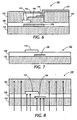
- Figs. 1-3 show illustrations of electronic devices 100, 120 and 130.
- a dielectric layer 108 is formed over a substrate 110 and over a gate electrode 109, and a semiconductor 106 is formed over the dielectric layer 108.
- an electrode 102 and an electrode 104 are located over the semiconductor 106.
- an electrode 122 and an electrode 124 are located between the semiconductor 112 and the substrate 110.
- an electrode 132 is located between the semiconductor 136 and the gate electrode 110, and an electrode 134 is located over the semiconductor 136.
- the electronic device 100 is said to be in a staggered configuration.
- the electronic device 120 is said to have a coplanar configuration.
- the electronic device 130 is said to have a hybrid configuration.
- devices with staggered geometries can have larger output currents than devices with coplanar geometries, such as Fig. 2 .
- an electronic device 120 with a coplanar configuration such as Fig. 2 , for example, is sometimes easier to manufacture than an electronic device 100 with staggered configurations, such as Fig. 1 , for example.
- an electronic device 120 with a coplanar configuration such as Fig. 2
- Fig. 4 is a cross section of an exemplary embodiment of an electronic device according to the method of the invention. Some of the elements in this figure are commonly numbered with elements previously discussed in connection with other figures. A duplicative discussion of those elements is omitted for the sake of simplicity.
- An electronic device 140 has a hybrid, i.e., both coplanar and staggered, configuration.
- an electrode 143 is formed over the dielectric layer 108, and a semiconductor 146 is formed over a portion of the electrode 143 and over a portion of the dielectric layer 108.
- a solution processable semiconductor 146 is printed over a portion of the electrode 143 and the dielectric layer 108.
- an electrode 147 is a metallic electrode formed over a portion of a via layer 144 and in electrical contact with an electrode 149 which is located over the semiconductor 146.
- the electrode 147 and the electrode 149 are made from the same material and form a continuous single electrode.
- the electrode 147 and the electrical contact 149 are made from a different material and are thus physically distinguishable.
- the electrical contact 149 is in a staggered configuration. Because the electrode 143 is between the semiconductor 146 and the dielectric layer 108, the electrode 143 is in a coplanar configuration in these various exemplary embodiments.
- an encapsulant 145 is located in a space between two or more portions of the via layer 144. Accordingly, Fig. 4 illustrates an exemplary embodiment of an electronic device 140 with a hybrid configuration.
- the gate electrode 109 is opaque to certain forms of radiation.
- Fig. 5 is a cross section of another exemplary embodiment of an electronic device according to the method of the invention. Some of the elements in this figure are commonly numbered with elements previously discussed in connection with other figures. A duplicative discussion of those elements is omitted for the sake of simplicity.
- the hybrid electronic device 150 includes a via layer portion 154 with a tapered sidewall 158 and a via layer portion 144 without a tapered sidewall.
- the tapered sidewall 158 allows for easier deposition of the metal electrode along the sidewall of the via layer 154.
- both sidewalls of the via layer are tapered.
- a semiconductor 156 is formed over a portion of the electrode 143 and over a portion of the dielectric layer 108, and is over a portion of the via layer portion 154.
- a electrode 157 is a metallic electrode formed over a portion of the via layer portion 154 and in contact with an electrical contact 159 which is located over a portion of the semiconductor 156.
- the electrode 157, the electrical contact 159, the semiconductor 156 and the encapsulant 155 have a tapered configuration.
- the encapsulant 155 is located in the space between the via layer portion 144 and the via layer portion 154.
- the electrode 157 and the electrical contact 159 are made from the same material. In various exemplary embodiments of the devices and methods according to this invention, the electrode 157 and the electrical contact 159 are made from a different material.
- Fig. 6 is a cross section of another exemplary embodiment of an electronic device 140 according to the method of the invention. Some of the elements in this figure are commonly numbered with elements previously discussed in connection with other figures. A duplicative discussion of those elements is omitted for the sake of simplicity.
- the electronic device 140 is a hybrid device and includes a via layer portion 142 that is not self-aligned with the electrode 143. In various exemplary embodiments of the devices and methods according to this invention, the via layer portion 142 partially covers the electrode 143, the dielectric layer 108, the semiconductor 146, and the electrode 149.
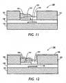
- Figs. 7-13 are cross sections of an electronic device 160 illustrating an exemplary embodiment of a method of manufacturing of an electronic device according to this invention. Some of the elements in these figures are commonly numbered with elements previously discussed in connection with other figures. A duplicative discussion of those elements is omitted for the sake of simplicity.
- a substrate 110, the electrode 109, the dielectric layer 108 and an electrode 143 are formed.
- a photosensitive liquid via layer 162 is formed over the dielectric layer 108 and the electrode 143.
- irradiation such as, for instance, ultraviolet light
- the radiation cures the photosensitive liquid via layer 162.
- the radiation is shone from the bottom of the gate electrode 110 as indicated in Fig. 8 .
- This so-called backside exposure allows for the curing of portions of the photosensitive liquid via layer 162 that are not blocked by an opaque body.
- the electrode 109 is, in various exemplary embodiments, opaque.
- the substrate 110 is, in various exemplary embodiments, transparent to the radiation.
- the electrode 143 and the gate electrode 109 are opaque to radiation.
- a portion of the photosensitive liquid via layer 162 is located above the electrode 143, or above the gate electrode 109, or both.
- that portion of the photosensitive liquid via layer 162 is not cured by the radiation.
- the electronic device 160 is said to be self-aligned.
- the portion of the photosensitive liquid via layer 162 that is above the source electrode 143 and above the top portion 109 of the gate electrode 110 is uncured. This portion of the photosensitive liquid via layer 162 is to be removed.
- the resultant structure in these various exemplary embodiments of the devices and methods of this invention, has a gate electrode 110 on which a dielectric layer 108 is formed.
- An electrode 143 is formed over the dielectric layer 108, and more than one portion of the via layer 162 is formed and cured over the dielectric layer 108.
- the portion of the dielectric layer 108 that is covered by the electrode 143 and the portion of the dielectric layer 108 that covers the top portion 109 of the gate electrode 110 is uncovered and provides a recess in the cured portion of the via layer 162.
- a semiconductor 146 is formed in a portion of the recess of the via layer 162 and covers a portion of the dielectric layer 108 and a portion of the electrode 143.
- a mask 164 is formed over a portion of the semiconductor 146 and over the portion of the electrode 143 that is not covered by the semiconductor 146.
- the mask 164 is printed.
- a metal layer 166 is deposited over the entire electronic device 160 and covers all portion of the via layer 162, an uncovered portion of the semiconductor 146 and the print resist 164.
- the metal layer 166 so deposited constitutes an electrode.
- an electrical device 190 includes an electrical contact 149 deposited on a portion of the semiconductor layer 146.
- the metal layer 166 is deposited over the electrical contact 149.
- the metal layer 166 is formed directly over the via layer 162 and over a portion of the semiconductor 146, for instance, by printing. In various exemplary embodiments of the devices and methods according to this invention, printing the metal layer 166 avoids using a mask such as, for example, the mask 164 illustrated in Figs. 11-12 , that needs to be subsequently removed.
- the print resist 164 is removed, thus uncovering the portion of the semiconductor 146 that is not covered by the electrode 166 or the electrical contact 149 and uncovering the portion of the electrode 143 that is not covered by the semiconductor 146.
- the resulting structure as illustrated in Figs. 13 and 14 , for example, is an electronic device 160 or 190 with a hybrid configuration where at least a portion of the electrode 143 is located under the semiconductor 146, and where at least a portion of the electrode 166 is located over the semiconductor 146.
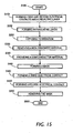
- Fig. 15 is a flow chart describing an exemplary embodiment of a method of fabrication of an electronic device according to this invention.
- the fabrication method starts in step S 100, then continues to step S 150, where a first and second electrical contacts are formed, along with a dielectric layer.
- the dielectric layer is located between the first and the second electrical contacts.
- the first electrical contact is a gate electrode.
- the second electrical contact is in a coplanar configuration with the semiconductor material.
- step S200 an electrically insulating layer is formed.
- the electrically insulating layer is formed over the dielectric layer and the first electrical contact.
- step S250 in various exemplary embodiments according to this invention, the first and second electrical contacts, the dielectric layer and a portion of the electrically insulating layer are exposed to radiation. In various exemplary embodiments according to this invention, the radiation comes from the side of the first electrical contact.
- the radiation to which the electrical device is subjected to is ultraviolet light.
- step S300 a portion of the electrically insulating layer that is not irradiated by the radiation is removed.
- a semiconductor material is provided.
- the semiconductor material is provided over a portion of the dielectric layer that is not covered by the electrically insulating layer.
- removing of the portion of the electrically insulating layer that was not irradiated by the radiation is performed by solvent washing.
- the removal of the portion of the electrically insulating layer creates a tapered wall.
- the semiconductor material is printed over the portion of the dielectric layer that is not covered by the electrically insulating layer.
- a mask is formed.
- the mask is formed over the second electrical contact and a portion of the semiconductor material.
- the mask prevents the second electrical contact and a portion of the semiconductor material from being in contact with any other material during subsequent steps of this method.
- the mask is a printed resist.
- step S450 a third electrical contact is formed.
- the third electrical contact is formed over at least a portion of the electrically insulating layer, the semiconductor material and the mask.
- step S500 a fourth electrical contact is formed over a portion of the third electrical contact and electrically insulating layer.
- the third electrical contact is formed via vapor deposition.
- the third and the fourth electrical contacts are made of the same material.
- step S500 is omitted.
- step S550 the mask is removed.
- the semiconductor material is a solution processable semiconductor and is printed and no mask is formed, no mask is removed. Control then proceeds to step S600, where the method ends.
Description
- This invention relates to electronic devices such as, for example, transistors and methods for fabricating the same.
- Electronic devices, such as, for example, transistors, have a multitude of uses. For example, low cost, large area arrays of thin-film transistors (TFTs) are important components in flat panel displays, electric paper, and imagers. In a pixel of a display, a TFT is used as an electrical switch to charge a pixel electrode that switches the display media from one state to another. A display backplane comprises an array of pixel elements that is used to address the display media. Amorphous silicon is often used as the active material in TFTs for these applications.
- Polymeric semiconductors have field effect mobilities of approximately 0.01-0.1 cm2V-1s-1 and are relatively simple to process due to their solubility and ease of forming continuous films. These field effect mobilities are typically lower than those obtained for amorphous silicon, ∼ 0.5-1.0 cm2V-1s-1.
- Additive and subtractive patterning techniques are sometimes used to fabricate patterned polymeric TFTs. Additive methods deposit only enough material for the desired pattern while subtractive methods deposit a blanket layer of material and remove the majority of it to define the pattern. Two subtractive methods for organic TFTs include photolithography and screen printing. Photolithography is a high-resolution, subtractive method for patterning, and is sometimes used to make complex circuits and displays with organic materials. An additive method sometimes used for fabrication of organic light emitting diodes, metal-organic-metal diodes, and TFTs is inkjet printing. Inkjet printing sometimes maintains registration by digital-image processing and precise spatial control of deposition.
- Generally, in a transistor, the source pad and the drain pad are configured in coplanar geometry. That is, the source pad and the drain pad are positioned over the gate electrode and under the semiconductor. Also, the source pad and the drain pad are sometimes configured in a staggered geometry. That is, the source and the drain pad are located over the semiconductor.
- The use of organic semiconductors can have advantages over amorphous silicon, especially for flexible electronics. Organic semiconductors are sometimes processed using low-cost techniques, are sometimes deposited at the low temperatures (e.g., lower than 150°C) required for plastic substrates, and tolerate mechanical stress. The development of micron-scale processing techniques for organic semiconductors is also beneficial.
- The use of organic semiconductors in TFTs in backplanes for displays is limited by their lower field effect mobility relative to amorphous silicon semiconductors. A TFT in a pixel element in a backplane provides current to place charge on a pixel electrode that causes a change in the display at that pixel. The existence of injection barriers at the contacts of organic TFTs can limit the maximum possible output current of the device and thus increases the time needed to place charge on the pixel electrode. In order to solve this problem, and to achieve the current required to charge a pixel electrode in a typical display, the electronic device, such as, for example, the transistor, is enlarged. This enlargement decreases the fill factor of the pixel in the display because of the increase in spatial area of the TFT in the pixel element.
The output current of the some organic electronic devices, such as, a thin film transistor, depends on the geometry of the device due to the presence of injection barriers at the source and drain contacts. Devices with staggered geometries can have larger output currents than devices with coplanar geometries due to decreased contact resistances. However, the manufacturing of devices with coplanar geometries is easier than the manufacturing of devices with staggered geometries, and is preferred for display applications. - Another problem commonly associated with organic devices such as, for example, transistors, is the type of material used as a via layer. The via layer reduces capacitive coupling between the addressing electrodes and the display media. Some via layers require processing steps, such as high temperature or reactive ion etching. These processing steps can damage the organic semiconductor.
-
EP 1367659 A2 describes an organic field effect transistor. In an organic field effect transistor, including, on a substrate having an insulating surface, at least a gate electrode a gate insulating film formed in contact with the gate electrode, an organic semiconductor film formed in contact with the gate insulating film, and at least a pair of source-drain electrodes formed in contact with the organic semiconductor film, a carrier generating electrode to which carriers can be injected in response to a gate signal is implanted within the organic semiconductor film. -
US 5,869,867 describes "FET semiconductor integrated circuit device having a planar element structure." In a semiconductor device, an extra wiring area generated by the connection of an upper layer wiring to an element on a semiconductor substrate is reduced to improve the level of integration, and the parasitic capacitances between the gate and the source-drain regions are reduced to enhance the performance of the circuit. A gate electrode is formed via a gate insulating film on a semiconductor layer formed in the semiconductor substrate. This semiconductor layer is for forming the source region and the drain region, where the source region and the drain region are formed on the left and right of the gate electrode with the gate electrode at the center. Wirings connected to the source region are formed on the same side of the gate electrode. Wirings connected to the drain region are formed on the opposite side of the gate electrode with the semiconductor layer in between. - It is the object of the present invention to improve an electronic device production particularly with regard to cost effective production and broad application in the field. This object is achieved by providing a method of fabricating an electronic device according to claim 1. Embodiments of the invention are set forth in the dependent claims.
- These and other features and advantages of this invention are described in, or are apparent from, the following detailed description of various exemplary embodiments of the systems and methods according to this invention.
- Various exemplary embodiments of devices and methods according to this invention will be described in detail with reference to the following figures, wherein:
-
Figs. 1-3 are cross sections of electronic devices; -
Fig. 4 is a cross section of an exemplary embodiment of an electronic device according to the method of the invention; -
Fig. 5 is a cross section of another exemplary embodiment of an electronic device according to the method of the invention; -
Fig. 6 is a cross section of another exemplary embodiment of an electronic device according to the method of the invention; -
Figs. 7-13 are cross sections of another exemplary embodiment of an electronic device illustrating an exemplary embodiment of a method of manufacturing an electronic device according to this invention; -
Fig. 14 is a cross section of another exemplary embodiment of an electronic device according to the method of the invention; and -
Fig. 15 is a flow chart describing an exemplary embodiment of a method of fabrication of an electronic device according to this invention. -
Figs. 1-3 show illustrations ofelectronic devices dielectric layer 108 is formed over asubstrate 110 and over agate electrode 109, and asemiconductor 106 is formed over thedielectric layer 108. InFig. 1 , anelectrode 102 and anelectrode 104 are located over thesemiconductor 106. InFig. 2 , anelectrode 122 and anelectrode 124 are located between thesemiconductor 112 and thesubstrate 110. InFig. 3 , anelectrode 132 is located between thesemiconductor 136 and thegate electrode 110, and an electrode 134 is located over thesemiconductor 136. Whenelectrode 102 and theelectrode 104 are located over thesemiconductor 106, such as inFig. 1 , for example, theelectronic device 100 is said to be in a staggered configuration. When theelectrode 122 and theelectrode 124 are located between thesemiconductor 112 and thegate electrode 110, as inFig. 2 , for example, theelectronic device 120 is said to have a coplanar configuration. When theelectrode 132 is located between thesemiconductor 136 and thegate electrode 110, as inFig. 3 , for example, theelectronic device 130 is said to have a hybrid configuration. - Typically, devices with staggered geometries, such as
Fig. 1 , for example, can have larger output currents than devices with coplanar geometries, such asFig. 2 . However, anelectronic device 120 with a coplanar configuration, such asFig. 2 , for example, is sometimes easier to manufacture than anelectronic device 100 with staggered configurations, such asFig. 1 , for example. Thus, anelectronic device 120 with a coplanar configuration, such asFig. 2 , is sometimes enlarged to compensate for the lower effective mobility. The enlargement of a coplanarelectronic device 120 at a pixel reduces a fill factor of the pixel, thus degrading the image of the display. -
Fig. 4 is a cross section of an exemplary embodiment of an electronic device according to the method of the invention. Some of the elements in this figure are commonly numbered with elements previously discussed in connection with other figures. A duplicative discussion of those elements is omitted for the sake of simplicity. - An
electronic device 140 has a hybrid, i.e., both coplanar and staggered, configuration. Thus, in various exemplary embodiments, anelectrode 143 is formed over thedielectric layer 108, and asemiconductor 146 is formed over a portion of theelectrode 143 and over a portion of thedielectric layer 108. - In various exemplary embodiments of the devices and methods according to this invention, a solution
processable semiconductor 146 is printed over a portion of theelectrode 143 and thedielectric layer 108. In various exemplary embodiments of the devices and methods according to this invention, anelectrode 147 is a metallic electrode formed over a portion of a vialayer 144 and in electrical contact with anelectrode 149 which is located over thesemiconductor 146. In various exemplary embodiments of the devices and methods according to this invention, theelectrode 147 and theelectrode 149 are made from the same material and form a continuous single electrode. In various exemplary embodiments of the devices and methods according to this invention, theelectrode 147 and theelectrical contact 149 are made from a different material and are thus physically distinguishable. In various exemplary embodiments, theelectrical contact 149 is in a staggered configuration. Because theelectrode 143 is between thesemiconductor 146 and thedielectric layer 108, theelectrode 143 is in a coplanar configuration in these various exemplary embodiments. - Also, in various exemplary embodiments, an
encapsulant 145 is located in a space between two or more portions of the vialayer 144. Accordingly,Fig. 4 illustrates an exemplary embodiment of anelectronic device 140 with a hybrid configuration. - In various exemplary embodiments, the
gate electrode 109 is opaque to certain forms of radiation. -
Fig. 5 is a cross section of another exemplary embodiment of an electronic device according to the method of the invention. Some of the elements in this figure are commonly numbered with elements previously discussed in connection with other figures. A duplicative discussion of those elements is omitted for the sake of simplicity. The hybridelectronic device 150 includes a vialayer portion 154 with atapered sidewall 158 and a vialayer portion 144 without a tapered sidewall. In various exemplary embodiments of the devices and methods according to this invention, the taperedsidewall 158 allows for easier deposition of the metal electrode along the sidewall of the vialayer 154. In various exemplary embodiments, both sidewalls of the via layer are tapered. - In various exemplary embodiments, a
semiconductor 156 is formed over a portion of theelectrode 143 and over a portion of thedielectric layer 108, and is over a portion of the vialayer portion 154. In various exemplary embodiments, aelectrode 157 is a metallic electrode formed over a portion of the vialayer portion 154 and in contact with anelectrical contact 159 which is located over a portion of thesemiconductor 156. In various exemplary embodiments, theelectrode 157, theelectrical contact 159, thesemiconductor 156 and theencapsulant 155 have a tapered configuration. Also, in various exemplary embodiments, theencapsulant 155 is located in the space between the vialayer portion 144 and the vialayer portion 154. - In various exemplary embodiments of the devices and methods according to this invention, the
electrode 157 and theelectrical contact 159 are made from the same material. In various exemplary embodiments of the devices and methods according to this invention, theelectrode 157 and theelectrical contact 159 are made from a different material. -
Fig. 6 is a cross section of another exemplary embodiment of anelectronic device 140 according to the method of the invention. Some of the elements in this figure are commonly numbered with elements previously discussed in connection with other figures. A duplicative discussion of those elements is omitted for the sake of simplicity. Theelectronic device 140 is a hybrid device and includes a vialayer portion 142 that is not self-aligned with theelectrode 143. In various exemplary embodiments of the devices and methods according to this invention, the vialayer portion 142 partially covers theelectrode 143, thedielectric layer 108, thesemiconductor 146, and theelectrode 149. -
Figs. 7-13 are cross sections of anelectronic device 160 illustrating an exemplary embodiment of a method of manufacturing of an electronic device according to this invention. Some of the elements in these figures are commonly numbered with elements previously discussed in connection with other figures. A duplicative discussion of those elements is omitted for the sake of simplicity. As shown inFig. 7 , for example, in various exemplary embodiments of the devices and methods according to this invention, asubstrate 110, theelectrode 109, thedielectric layer 108 and anelectrode 143 are formed. Then, in various exemplary embodiments of the devices and methods according to this invention, and as illustrated inFig. 8 , for example, a photosensitive liquid vialayer 162 is formed over thedielectric layer 108 and theelectrode 143. - In various exemplary embodiments of the devices and methods according to this invention, irradiation, such as, for instance, ultraviolet light, is shone on the photosensitive liquid via
layer 162, thesource electrode 143, thedielectric layer 108, and thesubstrate 110, andelectrode 109. In these exemplary embodiments, the radiation cures the photosensitive liquid vialayer 162. In various exemplary embodiments of the methods and devices according to this invention, the radiation is shone from the bottom of thegate electrode 110 as indicated inFig. 8 . This so-called backside exposure allows for the curing of portions of the photosensitive liquid vialayer 162 that are not blocked by an opaque body. Theelectrode 109 is, in various exemplary embodiments, opaque. Thesubstrate 110 is, in various exemplary embodiments, transparent to the radiation. Thus, only certain portions of the photosensitive liquid vialayer 162 are subjected to radiation in various exemplary embodiments as indicated by the arrows that pass through to the photosensitive liquid vialayer 162 from thegate electrode 109 inFig. 8 . - In various exemplary embodiments of the methods and devices according to this invention, the
electrode 143 and thegate electrode 109 are opaque to radiation. In these various exemplary embodiments of the methods and devices according to this invention, a portion of the photosensitive liquid vialayer 162 is located above theelectrode 143, or above thegate electrode 109, or both. In these various exemplary embodiments, that portion of the photosensitive liquid vialayer 162 is not cured by the radiation. In these various exemplary embodiments, theelectronic device 160 is said to be self-aligned. - In various exemplary embodiments of the devices and methods according to this invention, after curing is performed, some uncured material is removed as shown, for example, in
Fig. 9 . In various exemplary embodiments of the devices and methods according to this invention, this occurs, for instance, by solvent washing. Accordingly, in these exemplary embodiments, the portion of the photosensitive liquid vialayer 162 that is above thesource electrode 143 and above thetop portion 109 of thegate electrode 110 is uncured. This portion of the photosensitive liquid vialayer 162 is to be removed. - As illustrated in
Fig. 9 , for example, the resultant structure, in these various exemplary embodiments of the devices and methods of this invention, has agate electrode 110 on which adielectric layer 108 is formed. Anelectrode 143 is formed over thedielectric layer 108, and more than one portion of the vialayer 162 is formed and cured over thedielectric layer 108. In these various exemplary embodiments, the portion of thedielectric layer 108 that is covered by theelectrode 143 and the portion of thedielectric layer 108 that covers thetop portion 109 of thegate electrode 110 is uncovered and provides a recess in the cured portion of the vialayer 162. - In various exemplary embodiments of the devices and methods according to this invention, and as illustrated in
Fig. 10 , for example, asemiconductor 146 is formed in a portion of the recess of the vialayer 162 and covers a portion of thedielectric layer 108 and a portion of theelectrode 143. - In various exemplary embodiments of the devices and methods according to this invention, and as illustrated in
Fig. 11 , for example, amask 164 is formed over a portion of thesemiconductor 146 and over the portion of theelectrode 143 that is not covered by thesemiconductor 146. In various exemplary embodiments, themask 164 is printed. Accordingly, and as illustrated inFig. 12 , in various exemplary embodiments of the devices and methods of this invention, for example, ametal layer 166 is deposited over the entireelectronic device 160 and covers all portion of the vialayer 162, an uncovered portion of thesemiconductor 146 and the print resist 164. Themetal layer 166 so deposited constitutes an electrode. Referring toFig. 14 , in various exemplary embodiments, an electrical device 190 includes anelectrical contact 149 deposited on a portion of thesemiconductor layer 146. In various exemplary embodiments, themetal layer 166 is deposited over theelectrical contact 149. - In various exemplary embodiments of the devices and methods according to this invention, the
metal layer 166 is formed directly over the vialayer 162 and over a portion of thesemiconductor 146, for instance, by printing. In various exemplary embodiments of the devices and methods according to this invention, printing themetal layer 166 avoids using a mask such as, for example, themask 164 illustrated inFigs. 11-12 , that needs to be subsequently removed. - In various exemplary embodiments of the methods of this invention, and as illustrated in
Figs. 13 and 14 , for example, the print resist 164 is removed, thus uncovering the portion of thesemiconductor 146 that is not covered by theelectrode 166 or theelectrical contact 149 and uncovering the portion of theelectrode 143 that is not covered by thesemiconductor 146. In various exemplary embodiments of the methods and devices according to this invention, the resulting structure, as illustrated inFigs. 13 and 14 , for example, is anelectronic device 160 or 190 with a hybrid configuration where at least a portion of theelectrode 143 is located under thesemiconductor 146, and where at least a portion of theelectrode 166 is located over thesemiconductor 146. -
Fig. 15 is a flow chart describing an exemplary embodiment of a method of fabrication of an electronic device according to this invention. In various exemplary embodiments according to this invention, the fabrication method starts instep S 100, then continues to stepS 150, where a first and second electrical contacts are formed, along with a dielectric layer. In various exemplary embodiments according to this invention, the dielectric layer is located between the first and the second electrical contacts. In various exemplary embodiments according to this invention, the first electrical contact is a gate electrode. - In various exemplary embodiments according to this invention, the second electrical contact is in a coplanar configuration with the semiconductor material.
- Next, in step S200, an electrically insulating layer is formed. In various exemplary embodiments according to this invention, the electrically insulating layer is formed over the dielectric layer and the first electrical contact. Next, in step S250, in various exemplary embodiments according to this invention, the first and second electrical contacts, the dielectric layer and a portion of the electrically insulating layer are exposed to radiation. In various exemplary embodiments according to this invention, the radiation comes from the side of the first electrical contact.
- In various exemplary embodiments according to this invention, the radiation to which the electrical device is subjected to is ultraviolet light.
- Next, in step S300, a portion of the electrically insulating layer that is not irradiated by the radiation is removed. Next, in step S350, a semiconductor material is provided. In various exemplary embodiments according to this invention, the semiconductor material is provided over a portion of the dielectric layer that is not covered by the electrically insulating layer.
- In various exemplary embodiments according to this invention, removing of the portion of the electrically insulating layer that was not irradiated by the radiation is performed by solvent washing.
- In various exemplary embodiments according to this invention, the removal of the portion of the electrically insulating layer creates a tapered wall.
- In various exemplary embodiments according to this invention, the semiconductor material is printed over the portion of the dielectric layer that is not covered by the electrically insulating layer.
- Next, in step S400, a mask is formed. In various exemplary embodiments according to this invention, the mask is formed over the second electrical contact and a portion of the semiconductor material. In various exemplary embodiments according to this invention, the mask prevents the second electrical contact and a portion of the semiconductor material from being in contact with any other material during subsequent steps of this method.
- In various exemplary embodiments according to this invention, the mask is a printed resist.
- In various exemplary embodiments according to this invention, where the semiconductor material is printed, no mask is formed.
- Next, in step S450, a third electrical contact is formed. In various exemplary embodiments according to this invention, the third electrical contact is formed over at least a portion of the electrically insulating layer, the semiconductor material and the mask. Next, in step S500, a fourth electrical contact is formed over a portion of the third electrical contact and electrically insulating layer.
- In various exemplary embodiments according to this invention, the third electrical contact is formed via vapor deposition.
- In various exemplary embodiments according to this invention, the third and the fourth electrical contacts are made of the same material.
- In various exemplary embodiments according to this invention, step S500 is omitted.
- Next, in step S550, the mask is removed. In various exemplary embodiments according to this invention, where the semiconductor material is a solution processable semiconductor and is printed and no mask is formed, no mask is removed. Control then proceeds to step S600, where the method ends.
Claims (5)
- A method of fabricating an electronic device, comprising:forming a first electrical contact (109), a dielectric layer (108) and a second electrical contact (143), wherein the dielectric layer (108) is located between the first and the second electrical contacts and over the first electrical contact (109), the first electrical contact (109) and the second electrical contact (143) being opaque to an exposing radiation;forming an electrically insulating layer (162) over the dielectric layer (108) and the first electrical contact (109);exposing the second electrical contact (143), the dielectric layer (108), the first electrical contact (109) and a first portion of the electrically insulating layer (162) to the exposing radiation from the side of the first electrical contact (109);removing a second portion of the electrically insulating layer (162) that was not irradiated by the exposing radiation;providing a semiconductor material (146);forming a mask (164) over the second electrical contact (143) and a portion of the semiconductor material;forming a third electrical contact (149) over at least a portion of the electrically insulating layer (162), the semiconductor material and the maskremoving the mask, wherein the semiconductor material is formed over a portion of the dielectric layer (108) that is not under the electrically insulating layer (162) and on the second electrical contact (143), the semiconductor material in contact with the second and third electrical contacts (143,149).
- The method of claim 1, wherein exposing the second electrical contact (143), the dielectric layer (108), the first electrical contact (109) and a first portion of the electrically insulating layer (162) comprises exposing the second electrical contact (143), the dielectric layer (108), the first electrical contact (109) and a first portion of the electrically insulating layer (162) to ultraviolet light.
- The method of claim 1, wherein removing the second portion of the electrically insulating layer (162) that was not irradiated by the radiation comprises solvent washing the second portion of the electrically insulating layer (162) that was not irradiated by the radiation.
- The method of claim 1, wherein providing the semiconductor material over a portion of the dielectric layer (108) that is not under the electrically insulating layer (162) comprises printing a solution processable semiconductor over a portion of the dielectric layer (108) that is not under the electrically insulating layer (162).
- The method of claim 1, wherein forming the third electrical contact (149) over at least a portion of the electrically insulating layer (162), the semiconductor and the mask comprises chemical vapor depositing the third electrical contact (149) over at least a portion of the electrically insulating layer (162), the semiconductor and the mask.
Priority Applications (1)
| Application Number | Priority Date | Filing Date | Title |
|---|---|---|---|
| EP09168457A EP2128902A3 (en) | 2003-12-19 | 2004-12-15 | Thin film electronic device and methods for fabricating an electronic device |
Applications Claiming Priority (2)
| Application Number | Priority Date | Filing Date | Title |
|---|---|---|---|
| US10/739,189 US6921679B2 (en) | 2003-12-19 | 2003-12-19 | Electronic device and methods for fabricating an electronic device |
| US739189 | 2003-12-19 |
Related Child Applications (1)
| Application Number | Title | Priority Date | Filing Date |
|---|---|---|---|
| EP09168457A Division EP2128902A3 (en) | 2003-12-19 | 2004-12-15 | Thin film electronic device and methods for fabricating an electronic device |
Publications (3)
| Publication Number | Publication Date |
|---|---|
| EP1548837A2 EP1548837A2 (en) | 2005-06-29 |
| EP1548837A3 EP1548837A3 (en) | 2007-09-12 |
| EP1548837B1 true EP1548837B1 (en) | 2009-11-18 |
Family
ID=34552789
Family Applications (2)
| Application Number | Title | Priority Date | Filing Date |
|---|---|---|---|
| EP04029722A Expired - Fee Related EP1548837B1 (en) | 2003-12-19 | 2004-12-15 | Methods for fabricating an electronic thin film device |
| EP09168457A Ceased EP2128902A3 (en) | 2003-12-19 | 2004-12-15 | Thin film electronic device and methods for fabricating an electronic device |
Family Applications After (1)
| Application Number | Title | Priority Date | Filing Date |
|---|---|---|---|
| EP09168457A Ceased EP2128902A3 (en) | 2003-12-19 | 2004-12-15 | Thin film electronic device and methods for fabricating an electronic device |
Country Status (4)
| Country | Link |
|---|---|
| US (2) | US6921679B2 (en) |
| EP (2) | EP1548837B1 (en) |
| JP (1) | JP4319137B2 (en) |
| DE (1) | DE602004024164D1 (en) |
Families Citing this family (14)
| Publication number | Priority date | Publication date | Assignee | Title |
|---|---|---|---|---|
| US20060012742A1 (en) * | 2004-07-16 | 2006-01-19 | Yaw-Ming Tsai | Driving device for active matrix organic light emitting diode display and manufacturing method thereof |
| US7784173B2 (en) * | 2005-12-27 | 2010-08-31 | Palo Alto Research Center Incorporated | Producing layered structures using printing |
| US7816146B2 (en) * | 2005-12-27 | 2010-10-19 | Palo Alto Research Center Incorporated | Passive electronic devices |
| US8637138B2 (en) | 2005-12-27 | 2014-01-28 | Palo Alto Research Center Incorporated | Layered structures on thin substrates |
| JP5458296B2 (en) * | 2006-10-27 | 2014-04-02 | 国立大学法人岩手大学 | MICRO-PROCESSED STRUCTURE, PROCESSING METHOD THEREOF, ELECTRONIC DEVICE, AND MANUFACTURING METHOD THEREOF |
| US7576000B2 (en) | 2006-12-22 | 2009-08-18 | Palo Alto Research Center Incorporated | Molded dielectric layer in print-patterned electronic circuits |
| US8258021B2 (en) | 2007-10-26 | 2012-09-04 | Palo Alto Research Center Incorporated | Protecting semiconducting oxides |
| US7755156B2 (en) * | 2007-12-18 | 2010-07-13 | Palo Alto Research Center Incorporated | Producing layered structures with lamination |
| US7586080B2 (en) * | 2007-12-19 | 2009-09-08 | Palo Alto Research Center Incorporated | Producing layered structures with layers that transport charge carriers in which each of a set of channel regions or portions operates as an acceptable switch |
| US8283655B2 (en) * | 2007-12-20 | 2012-10-09 | Palo Alto Research Center Incorporated | Producing layered structures with semiconductive regions or subregions |
| DE102011085114B4 (en) * | 2011-10-24 | 2016-02-18 | Fraunhofer-Gesellschaft zur Förderung der angewandten Forschung e.V. | Thin film transistor |
| CN102779783B (en) * | 2012-06-04 | 2014-09-17 | 北京京东方光电科技有限公司 | Pixel structure, as well as manufacturing method and display device thereof |
| EP2811525B1 (en) * | 2013-03-14 | 2019-02-13 | Karlsruher Institut für Technologie | Electrochemically-gated field-effect transistor, method for its manufacture, its use, and electronics comprising said field- effect transistor |
| CN108428796B (en) * | 2017-02-14 | 2021-10-15 | 元太科技工业股份有限公司 | Organic thin film transistor and display device |
Family Cites Families (15)
| Publication number | Priority date | Publication date | Assignee | Title |
|---|---|---|---|---|
| US27082A (en) * | 1860-02-07 | Improvement in sewing-machines | ||
| US5032883A (en) * | 1987-09-09 | 1991-07-16 | Casio Computer Co., Ltd. | Thin film transistor and method of manufacturing the same |
| US5017989A (en) | 1989-12-06 | 1991-05-21 | Xerox Corporation | Solid state radiation sensor array panel |
| JPH09260669A (en) * | 1996-03-19 | 1997-10-03 | Nec Corp | Semiconductor device and manufacture thereof |
| JPH09307114A (en) * | 1996-05-17 | 1997-11-28 | Fujitsu Ltd | Thin film transistor, manufacture thereof and liquid crystal display device |
| DE69839935D1 (en) * | 1997-11-25 | 2008-10-09 | Nec Lcd Technologies Ltd | Active matrix liquid crystal display and its manufacturing method |
| KR100310179B1 (en) * | 1999-04-01 | 2001-10-29 | 구본준, 론 위라하디락사 | X-ray image sensor and a method for fabricating the same |
| US6545291B1 (en) | 1999-08-31 | 2003-04-08 | E Ink Corporation | Transistor design for use in the construction of an electronically driven display |
| US7439096B2 (en) * | 2001-02-21 | 2008-10-21 | Lucent Technologies Inc. | Semiconductor device encapsulation |
| JP2004527124A (en) | 2001-04-10 | 2004-09-02 | サーノフ コーポレイション | Method and apparatus for providing high performance active matrix pixels using organic thin film transistors |
| US6872320B2 (en) | 2001-04-19 | 2005-03-29 | Xerox Corporation | Method for printing etch masks using phase-change materials |
| JP4841751B2 (en) * | 2001-06-01 | 2011-12-21 | 株式会社半導体エネルギー研究所 | Organic semiconductor device and manufacturing method thereof |
| EP1367659B1 (en) * | 2002-05-21 | 2012-09-05 | Semiconductor Energy Laboratory Co., Ltd. | Organic field effect transistor |
| US20030227014A1 (en) * | 2002-06-11 | 2003-12-11 | Xerox Corporation. | Process for forming semiconductor layer of micro-and nano-electronic devices |
| US6639531B1 (en) * | 2002-09-27 | 2003-10-28 | Cirrus Logic, Inc. | Cascaded noise shaping circuits with low out-of-band noise and methods and systems using the same |
-
2003
- 2003-12-19 US US10/739,189 patent/US6921679B2/en not_active Expired - Fee Related
-
2004
- 2004-12-15 EP EP04029722A patent/EP1548837B1/en not_active Expired - Fee Related
- 2004-12-15 EP EP09168457A patent/EP2128902A3/en not_active Ceased
- 2004-12-15 DE DE602004024164T patent/DE602004024164D1/en active Active
- 2004-12-17 JP JP2004366903A patent/JP4319137B2/en not_active Expired - Fee Related
-
2005
- 2005-03-04 US US11/071,305 patent/US7405424B2/en active Active
Also Published As
| Publication number | Publication date |
|---|---|
| US20050208695A1 (en) | 2005-09-22 |
| US20050133788A1 (en) | 2005-06-23 |
| EP2128902A2 (en) | 2009-12-02 |
| EP2128902A3 (en) | 2010-01-06 |
| US7405424B2 (en) | 2008-07-29 |
| DE602004024164D1 (en) | 2009-12-31 |
| JP2005183990A (en) | 2005-07-07 |
| EP1548837A2 (en) | 2005-06-29 |
| EP1548837A3 (en) | 2007-09-12 |
| US6921679B2 (en) | 2005-07-26 |
| JP4319137B2 (en) | 2009-08-26 |
Similar Documents
| Publication | Publication Date | Title |
|---|---|---|
| US7405424B2 (en) | Electronic device and methods for fabricating an electronic device | |
| EP1163695B1 (en) | Method of manufacturing a transistor | |
| JP4907975B2 (en) | Large area electronic devices with high and low resolution patterned film features. | |
| US9564537B2 (en) | Array substrate and method for manufacturing the same | |
| US8269219B2 (en) | Printed TFT and TFT array with self-aligned gate | |
| EP1815541A1 (en) | Self-aligned process to manufacture organic transistors | |
| CN103988307A (en) | Self-aligned metal oxide tft with reduced number of masks | |
| US20070235733A1 (en) | Transistor, pixel electrode substrate, electro-optic device, electronic apparatus, and process for manufacturing semiconductor element | |
| KR100803426B1 (en) | Substrate and process for producing the same | |
| US9401431B2 (en) | Double self-aligned metal oxide TFT | |
| US6686229B2 (en) | Thin film transistors and method of manufacture | |
| US20060183263A1 (en) | Structure and Manufacturing Method of An Image TFT Array | |
| WO2001044867A1 (en) | Method of manufacturing an active matrix device | |
| US20070295960A1 (en) | Semiconductor device, electro-optical device, electronic apparatus, and method of producing semiconductor device | |
| JP2005123438A (en) | Thin film transistor, manufacturing method thereof, thin film transistor array, display device and sensor equipment | |
| KR100817215B1 (en) | Self-aligned organic field effect transistors and manufacturing method the same | |
| US5605845A (en) | Manufacture of electronic devices comprising thin-film transistors having self-aligned plural gates | |
| US8519393B2 (en) | Thin film transistor array panel and manufacturing method thereof | |
| KR20070069057A (en) | Method of manufacturing semiconductor device, semiconductor device and electronic appratus therefore | |
| KR20060124306A (en) | Wiring for display device and thin film transistor array panel including the same and method for manufacturing thereof | |
| CN112335048A (en) | Transistor array | |
| KR20060087710A (en) | Thin film transistor substrate |
Legal Events
| Date | Code | Title | Description |
|---|---|---|---|
| PUAI | Public reference made under article 153(3) epc to a published international application that has entered the european phase |
Free format text: ORIGINAL CODE: 0009012 |
|
| AK | Designated contracting states |
Kind code of ref document: A2 Designated state(s): AT BE BG CH CY CZ DE DK EE ES FI FR GB GR HU IE IS IT LI LT LU MC NL PL PT RO SE SI SK TR |
|
| AX | Request for extension of the european patent |
Extension state: AL BA HR LV MK YU |
|
| PUAL | Search report despatched |
Free format text: ORIGINAL CODE: 0009013 |
|
| AK | Designated contracting states |
Kind code of ref document: A3 Designated state(s): AT BE BG CH CY CZ DE DK EE ES FI FR GB GR HU IE IS IT LI LT LU MC NL PL PT RO SE SI SK TR |
|
| AX | Request for extension of the european patent |
Extension state: AL BA HR LV MK YU |
|
| 17P | Request for examination filed |
Effective date: 20080312 |
|
| AKX | Designation fees paid |
Designated state(s): DE FR GB |
|
| 17Q | First examination report despatched |
Effective date: 20080528 |
|
| RTI1 | Title (correction) |
Free format text: METHODS FOR FABRICATING AN ELECTRONIC THIN FILM DEVICE |
|
| GRAP | Despatch of communication of intention to grant a patent |
Free format text: ORIGINAL CODE: EPIDOSNIGR1 |
|
| RIC1 | Information provided on ipc code assigned before grant |
Ipc: H01L 51/00 20060101ALI20090504BHEP Ipc: H01L 29/417 20060101ALI20090504BHEP Ipc: H01L 51/05 20060101AFI20090504BHEP |
|
| GRAS | Grant fee paid |
Free format text: ORIGINAL CODE: EPIDOSNIGR3 |
|
| GRAA | (expected) grant |
Free format text: ORIGINAL CODE: 0009210 |
|
| AK | Designated contracting states |
Kind code of ref document: B1 Designated state(s): DE FR GB |
|
| REG | Reference to a national code |
Ref country code: GB Ref legal event code: FG4D |
|
| REF | Corresponds to: |
Ref document number: 602004024164 Country of ref document: DE Date of ref document: 20091231 Kind code of ref document: P |
|
| PLBE | No opposition filed within time limit |
Free format text: ORIGINAL CODE: 0009261 |
|
| STAA | Information on the status of an ep patent application or granted ep patent |
Free format text: STATUS: NO OPPOSITION FILED WITHIN TIME LIMIT |
|
| 26N | No opposition filed |
Effective date: 20100819 |
|
| REG | Reference to a national code |
Ref country code: FR Ref legal event code: PLFP Year of fee payment: 12 |
|
| PGFP | Annual fee paid to national office [announced via postgrant information from national office to epo] |
Ref country code: DE Payment date: 20151119 Year of fee payment: 12 Ref country code: GB Payment date: 20151125 Year of fee payment: 12 |
|
| PGFP | Annual fee paid to national office [announced via postgrant information from national office to epo] |
Ref country code: FR Payment date: 20151123 Year of fee payment: 12 |
|
| REG | Reference to a national code |
Ref country code: DE Ref legal event code: R119 Ref document number: 602004024164 Country of ref document: DE |
|
| GBPC | Gb: european patent ceased through non-payment of renewal fee |
Effective date: 20161215 |
|
| REG | Reference to a national code |
Ref country code: FR Ref legal event code: ST Effective date: 20170831 |
|
| PG25 | Lapsed in a contracting state [announced via postgrant information from national office to epo] |
Ref country code: FR Free format text: LAPSE BECAUSE OF NON-PAYMENT OF DUE FEES Effective date: 20170102 |
|
| PG25 | Lapsed in a contracting state [announced via postgrant information from national office to epo] |
Ref country code: GB Free format text: LAPSE BECAUSE OF NON-PAYMENT OF DUE FEES Effective date: 20161215 Ref country code: DE Free format text: LAPSE BECAUSE OF NON-PAYMENT OF DUE FEES Effective date: 20170701 |