TECHNICAL FIELD
-
The present invention relates to a group III nitride
semiconductor film and a method of fabricating the same.
BACKGROUND ART
-
A group III nitride semiconductor film, for example, a mixed
crystal AlxGayIn1-x-yN (0≤x≤1, 0≤y≤1 and 0≤x+y≤1) made by mixing
GaN, Al or In at a suitable ratio has an energy gap ranging from
0.75 eV to 6.288 eV and is a direct transition type semiconductor.
Accordingly, the group III nitride semiconductor has eminent
characteristics in a luminous efficiency as compared with
materials belonging to an indirect transition type such as SiC
and is suitable for a material for light emitting diodes, laser
diodes, ultraviolet ray detecting elements and the like.
-
No methods have been known of fabricating a group III nitride
semiconductor film having fine quality, large thickness and large
area. Accordingly, a buffer layer of AlN or GaN is formed on
a substrate differing from the group III nitride semiconductor
film in a lattice constant and a thermal expansion coefficient,
such as sapphire, SiC, Si or GaAs. GaN is formed on the buffer
layer by an epitaxial growth method. For example, a known
light-emitting chip of blue LED employing GaN has a double
heterostructure in which a GaN buffer layer, n-type GaN layer,
n-type GaAlN layer, InGaN layer, p-type GaAlN layer and p-type
GaN layer are sequentially laminated on a sapphire substrate.
-
However, in the method of fabricating a group III nitride
semiconductor film on the sapphire substrate, a GaN film has a
large number of lattice defects due to a difference in the lattice
constant between a grown GaN film and the substrate. Accordingly,
in order that a group III nitride semiconductor film having fewer
lattice defects and a large film thickness may be made, an epitaxial
lateral overgrowth (ELO) using a stripe mask (for example,
JP-A-10-312971) or re-growth after partial elimination by etching
(PENDEO) is carried out in order that a group III nitride
semiconductor film having fewer lattice defects and a large film
thickness may be made.
-
Thus, ELO and PENDEO have been devised to make a GaN film
with fewer lattice defects. However, spaces between growth
starting parts are in the order of micrometers and relatively
larger. Accordingly, the film is grown while lattice defects
are transferred from lower layers to upper ones, whereupon a
uniform crystal film involving fewer lattice defects cannot be
obtained. Furthermore, a high purity group III nitride
semiconductor film cannot be obtained in ELO by the influence
of contamination by SiO2 which is a mask material.
-
Furthermore, no electrode can be provided on an upper side
of the sapphire substrate since sapphire serving as the substrate
material is electrically insulating. Accordingly, a part of the
semiconductor film needs to be exposed in order that electrodes
may be provided on the group III nitride semiconductor film. For
example, when the foregoing double hetero structure is exemplified,
parts of the p-type GaN layer which is an uppermost layer, p-type
GaAlN layer, InGaN layer and n-type GaAlN layer are eliminated
in this order. An n-electrode is provided on the surface of the
n-type GaN layer. A p-electrode is provided on the surface of
the uppermost p-type GaN layer. Thus, etching needs to be carried
out so that a part of the semiconductor is eliminated. The etching
process results in damage in the crystal, constituting a cause
for reduction in the performance of a semiconductor device.
-
Furthermore, GaN has a larger refractive index than glass
or the like (for example, glass has a refractive index of 1.5
and GaN 2.5) and accordingly, reflection on an interface between
crystal and space results in a problem. More specifically, when
GaN is used, the aforesaid problem is a loss in emitted light
in a light-emitting element and a reduction in light detecting
sensitivity in a light detecting element. Thus, the aforesaid
problem is an obstacle to making full use of each element's
performance, whereupon it is difficult to manufacture a
light-emitting element or light detecting element each having
superior characteristics. Processes as multilayer film coating
have conventionally been employed to overcome the problem.
However, when the device is used with a shorter frequency than
the ultraviolet region, it is difficult to maintain the properties
of coating since a coating material which is an organic substance
is serially damaged. Furthermore, in a process for making a mask
pattern by photolithography, light employed for exposure has a
wavelength of 248 nm of a KrF excimer laser at the shortest.
Accordingly, it is impossible to make a fine mask of several nm
to about one hundred nm on the surface of GaN.
-
The present invention was made in view of the foregoing and
an object thereof is to provide a group III nitride semiconductor
film having fewer lattice defects and a large film thickness and
a method of fabricating the same, and another object is to provide
a group III nitride semiconductor film having an eminent light
detecting or emitting property and a method of fabricating the
same.
DISCLOSURE OF THE INVENTION
-
The inventors were devoted to the study of a method of
fabricating a group III nitride semiconductor film such as a GaN
compound semiconductor film and found that the object was achieved
by forming a pillar-shaped structure (nano-pillars) in the order
of nanometer consisting of a group III nitride semiconductor and
depositing another group III nitride semiconductor film on the
nano-pillars, thereby completing the present invention
basically.
-
A first invention is a method of fabricating a group III nitride
semiconductor film characterized by 1 ○ a nano-pillar fabricating
step of fabricating nano-pillars by dry-etching a group III nitride
semiconductor film while an etching retarding substance having
a smaller etching rate than the group III nitride semiconductor
is present on a surface of the group III nitride semiconductor
(a lower layer) to be etched, and 2 ○ a depositing step of depositing
another group III nitride semiconductor (an upper layer) on the
nano-pillars, thereby making the group III nitride semiconductor
film.
-
It is preferable that the etching retarding substance is
placed as a solid substance in an etching chamber in the 1 ○
nano-pillar fabricating step so as to be exposed to an etching
gas in dry etching.
-
Furthermore, it is preferable that the etching retarding
substance is SiO2.
-
A second invention is a group III nitride semiconductor film
characterized in that a number of lattice defects ranges from
102/cm2 to 108/cm2 and a film thickness thereof ranges from 1 µm
to 104 µm. It is preferable that the group III nitride semiconductor
film is fabricated by separating, at the nano-pillars, the group
III nitride semiconductor film fabricated by the first invention.
-
A third invention is a methodof fabricating a group III nitride
semiconductor film,characterized by 3 ○ anano-pillarfabricating
step of dry-etching a group III nitride semiconductor film while
an etching retarding substance having a smaller etching rate than
the group III nitride semiconductor film is present on a surface
of the group III nitride semiconductor film, thereby fabricating
nano-pillars.
-
The fabricated nano-pillars may be filled with ITO (Indium
Tin Oxide), Al2O3, SiO2 or the like. It is preferable that the
substances filling the nano-pillars have respective refractive
indexes ranging from 1 to 2.5. In this case, it is preferable
that for example, a chemical etching is carried out in order that
the etching retarding substance on the nano-pillar surfaces may
be eliminated so that the elimination contributes to smooth
formation of a filling layer. As a method of filling the
nano-pillars is exemplified a metal organic vapor phase epitaxy
method (MOVPE), a hydride VPE method (HVPE), a molecular beam
epitaxy method (MBE) or the like.
-
The present invention will be described in more detail. A
material for the group III nitride semiconductor film fabricated
by the present invention is a group III-V semiconductor containing
a group III element such as GaN, GaAlN, InGaN or the like (gallium,
for example) and can generally be represented by chemical formula,
AlxGayIn1-x-yN (0≤x≤1, 0≤y≤1 and 0≤x+y≤1). These group III nitride
semiconductor films may be pure or doped with impurity, which
may be a p-type or n-type.
-
Furthermore, the group III nitride semiconductor film may
have a monolayer or multilayer structure. When the group III
nitride semiconductor film has a multilayer structure, all the
layers may be formed of the group III nitride semiconductor film
or at least one of the layers may be formed of the group III nitride
semiconductor film. Furthermore, the group III nitride
semiconductor film may be formed on a substrate of sapphire or
the like, for example. The present invention may be employed
for fabrication of a group III nitride semiconductor film having
a multilayer structure such as a double heterostructure, for
example.
-
The "etching retarding substance" is a substance having a
smaller etching rate than the group III nitride semiconductor which
is substantially a target substance, when the dry etching is
carried out. When the etching retarding substance is present
on the surface of the group III nitride semiconductor, a dry-etching
speed becomes non-uniform on the target surface. Accordingly,
etching is conducted slower on a part on which the etching retarding
substance is present than another part on which the etching
retarding substance is absent, whereupon a rugged structure
(nano-pillars) is formed on the target surface (as will be
described in detail later). As a concrete etching retarding
substance are exemplified quartz (SiO2), sapphire, nickel,
organic resist or the like.
-
The "dry etching" is an etching method making use of gas
discharge, differing from a chemical wet etching and includes
for example, a reactive ion etching (RIE) , an electron cyclotron
resonance etching (ECR) and an inductive coupling plasma etching
(ICP).
-
"Present" means that the etching retarding substance is
present on the surface of the group III nitride semiconductor in
the order of nanometer (a range smaller than 1 µm). A method
to obtain such a condition includes, for example, (i) a method
of conducting etching while a solid etching retarding substance
is placed in a chamber where the etching is conducted, whereby
the etching retarding substance is produced by the sputtering
in the etching chamber to be adhered to the surface of the group
III nitride semiconductor, (ii) a method of causing the etching
retarding substance to flow into the etching chamber, (iii) a
method of previously dusting the etching retarding substance in
the nanometer order onto the surface of the group III nitride
semiconductor (the lower layer in the 1 ○ nano-pillar fabricating
step) on which nano-pillars are to be formed.
-
The "nano-pillars" means a structure in which a plurality
of small pillars each having a section sized in the nanometer
order protrude. The nano-pillars have an exceedingly small
probability of lattice defects which are present on the etched
group III nitride semiconductor film. Moreover, the aforesaid
lattice defects, even if the nano-pillars involve them, do not
almost affect another group III nitride semiconductor film
deposited with the top of each nano-pillar serving as a core of
crystal growth. Furthermore, the light reflectance is reduced
by providing nano-pillars on the surface of the group III nitride
semiconductor film, whereby the light transmittance is improved.
Accordingly, when a light emitting or light detecting device is
manufactured using the group III nitride semiconductor film having
the nano-pillars, the device has a better quality than the
conventional one, that is, the light emitting efficiency is
improved in the light emitting device and the sensitivity is
improved in the light detecting device.
-
In the first or third invention, when the group III nitride
semiconductor is dry-etched in the nano-pillar fabricating step
(1 ○ or 3 ○), the dry-etching is carried out while the etching
retarding substance is present on the surface of the target group
III nitride semiconductor. Since the etching retarding substance
has a lower etching rate than the group III nitride semiconductor,
the etching retarding substance serves as a micro-mask on a part
of the surface to which the etching retarding substance is adherent,
so that a micro rugged structure is formed at an initial stage
of the etching. Since the electric field is higher in a slightly
convex portion than in the concave portion, the subsequently
ionized etching retarding substance will adhere to the convex
portion with higher probability. Thus, it is supposed that
re-adherence of the etching retarding substance and etching by
an etching gas plasma repeatedly progress, whereby the
nano-pillars are fabricated.
-
Describing a more concrete method, a group III nitride
semiconductor film is placed on an upper side of one of a pair
of positive and negative electrodes (parallel plate electrodes,
for example) installed in an etching chamber where the internal
pressure has been reduced to the order of 10-4 Pa, and high frequency
power is applied to the aforesaid electrodes so that plasma is
generated from a plasma generating gas while the etching retarding
substance is present in the etching chamber. The group III nitride
semiconductor film is etched by the plasma, whereby nano-pillars
are fabricated. Most of the fabricated nano-pillars have a
dimension of not more than about 100 nm and in addition, a space
(gap) between adjacent nano-pillars can be ranged from several
tens nm to about 100 nm on the average. Accordingly, the
nano-pillar and the gap can repeatedly be constructed at a distance
of about 100 nm. Then, nano-pillars whose maximum number is about
1×10⁶ are constructed for every 1 cm, and accordingly, nano-pillars
whose maximum number is about 1×10¹² can be fabricated for every
1 cm2.
-
In the nano-pillar fabricating step (1 ○ or 3 ○), a type of
the etching gas is not dependent but any type of gas which can
generally be used in the dry etching of the group III nitride
semiconductor may be employed. For example, an inert gas such
as a Cl2 gas, BCl3 gas, SiCl4 gas, SF6 gas CHF3 gas, CF4 gas, CCl2F2
gas, CCl4 gas, Ar or the like may be employed individually or
in a mixture. In this case, it is preferable that a flow rate
of gas ranges from 0.1 ml/min to 500 ml/min.
-
Furthermore, in the nano-pillar fabricating step (1 ○ or 3 ○),
it is preferable that the etching retarding substance as a solid
is selected and placed in the etching chamber so as to be exposed
to an etching gas plasma during the dry etching. As a result,
the etching retarding substance is scattered into plasma by the
sputtering effect during the etching and moreover, part of the
scattered substance is ionized such that the etching retarding
molecular adheres to the surface of the group III nitride
semiconductor, whereupon the target group III nitride
semiconductor is etched into nano-pillars. Since the etching
retarding substance is placed in the etching chamber in the
invention, condition control in the etching can be rendered
easier.
-
As a form of the solid etching retarding substance used in
the nano-pillar fabricating step (1 ○ or 3 ○) is exemplified a form
of wafer or a form of chip cut out of the wafer. Furthermore,
as a general placing manner, the group III nitride semiconductor
can be placed on the upper side of the solid etching retarding
substance or the solid etching retarding substance can be placed
near the group III nitride semiconductor. Further, an exposure
area of the solid etching retarding substance (that is, an area
of the solid etching retarding substance etched by the plasma)
can suitably be determined according to the size of the group
III nitride semiconductor to be etched and a distribution density
of nano-pillars. More specifically, it is preferable that the
exposure area of the solid etching retarding substance ranges
from 2 to 100 relative to an exposure area of the group III nitride
semiconductor. Further, when SiO2 is used as the etching
retarding substance, conventionally generally used mask
substances can be used and accordingly, the invention can be put
into practice without large changes in the conventional
constitution.
-
In the nano-pillar fabricating step (1 ○ or 3 ○), an internal
pressure of the etching chamber in the dry etching is similar
to that in the normal dry etching and can be set in a range from
0.01 Pa to 100 Pa, for example. Furthermore, a high frequency
power density is the same as in the normal dry etching. For example,
an electric power density can be set to range from 0.01 W/cm2
to 10 W/cm2. In the invention, it is preferable that silicon
dioxide (SiO2) is used as a mask applied to the surface of the
group III nitride semiconductor. The reason for this is that
silicon dioxide generally has a property that it cannot easily
be etched by an etching gas plasma (for example, chlorine gas
plasma).
-
In the first invention, another group III nitride
semiconductor (an upper layer) is deposited on the nano-pillars
which serves as cores comprising thus formed group III nitride
semiconductor (a lower layer) (2 ○a depositing step). In this
case, it is preferable that for example, a chemical etching is
carried out in order that the etching retarding substance on the
nano-pillar surfaces may be eliminated completely so that the
elimination contributes to smooth formation of the upper layer.
As a method of depositing the upper layer is exemplified a metal
organic vapor phase epitaxy method (MOVPE), a hydride VPE method
(HVPE), a molecular beam epitaxy method (MBE) or the like.
-
Further according to the first invention, the probability
that lattice defects present in the lower layer group III nitride
semiconductor remains present in the nano-pillars is exceedingly
small. Accordingly, the group III nitride semiconductor (an upper
layer) involving fewer lattice defects is deposited on an upper
face of the lower layer. In addition to this, the upper layer
is deposited on the nano-pillars comprising the group III nitride
semiconductor having the same physical properties such as the
lattice constant as the upper layer. Accordingly, the upper layer
is exceedingly stable as compared with the case where the upper
layer is deposited on an upper face of the substance having a
different lattice constant and thermal expansion coefficient such
as sapphire as in the conventional structure. Consequently, the
group III nitride semiconductor film having such a large film
thickness as was not able to be obtained conventionally. Thus,
by separating the nano-pillars from the upper layer by the process
of the present invention, the group III nitride semiconductor film
can be provided in which the number of lattice defects ranges
from 102/cm2 to 108/cm2 or more preferably, from 102/cm2 to 105/cm2
or further more preferably, from 102/cm2 to 103/cm2 and the film
thickness ranges from 0.1 µm to 104 µm or more preferably, from
1 µm to 104 µm or further more preferably 1 µm to 5×102 µm or still
further more preferably, from 1 µm to 104 µm.
-
A method of separating the nano-pillars from the upper layer
includes physical methods (for example, cutting by a sharp blade
or a cutter provided with a substance having a high hardness,
such as diamond or breaking the nano-pillars by application of
impulse or shearing stress) and chemical methods (melting only
the nano-pillars by soaking them in an etchant, thereby separating
the nano-pillars). Furthermore, it is preferable that the face
on which the nano-pillars are located is ground and flattened.
-
Further another group III nitride semiconductor film is grown
on the aforesaid semiconductor film serving as a substrate,
whereupon optical devices such as light emitting elements, bipolar
devices such as transistors and unipolar devices such as FET's
can be fabricated.
-
The third invention is a process of fabricating a light
emitting device including nano-pillars on the surface of the group
III nitride semiconductor film or a light detecting device. The
3 ○ nano-pillar fabricating step is carried out in the same manner
as in the 1 ○ nano-pillar fabricating step in the first invention.
The nano-pillars are provided on the surface of the group III nitride
semiconductor film in the present invention. Furthermore, in
the 3 ○ nano-pillar fabricating step, a suitable mask is provided
on the surface such that a predetermined pattern can be formed.
-
According to the first invention, the group III nitride
semiconductor film having no stress-strain, fewer lattice defects
and a large thickness can efficiently be fabricated in a short
period of time. Furthermore, the mixed crystal involving fewer
lattice defects, AlxGayIn1-x-yN (0≤x≤1, 0≤y≤1 and 0≤x+y≤1), is
formed on the aforesaid group III nitride semiconductor film,
whereby a multilayer film can be formed. Consequently, light
emitting and detecting devices having high light emitting and
detecting efficiencies respectively can be provided.
-
Furthermore, the group III nitride semiconductor film (the
upper layer) fabricated in accordance with the present invention
is separated, with the nano-pillars serving as a boundary, ) from
the sapphire substrate, the buffer layer and the group III nitride
semiconductor film (the lower layer) involving stress-strain and
a large number of lattice defects, all of which are present on
the lower layer, whereby the group III nitride semiconductor film
can be fabricated into a group III nitride semiconductor film.
Consequently, a back electrode (which is conventionally provided
on the semiconductor film nearer to the sapphire substrate) can
easily be fabricated and steps can be simplified. Additionally,
the freedom in the design such as an increase in an effective
light emitting area can be increased.
-
According to the third invention, the nano-pillars having
a distribution density of 106/cm2 to 1012/cm2 can easily be provided
although these nano-pillars cannot conventionally be fabricated
stably. Furthermore, the group III nitride semiconductor film
fabricated in accordance with the present invention has an
improved light reflectance and transmittance (that is, the
reflectance is reduced and the transmittance is increased).
Consequently, the light emitting device with an improved
reflectance and transmittance can be provided.
-
Particularly when AlGaN or AlN each containing Al as the
group III nitride semiconductor is used, it is supposed that the
reflectance can be improved regarding short waves (for example,
about 200 nm) and accordingly, desirable optical devices can be
provided with respect to light in the ultraviolet region although
such optical devices were not conventionally provided.
BRIEF DESCRIPTION OF THE DRAWINGS
-
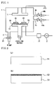
- FIG. 1 is a sectional view of an etching apparatus which
can be used in the practice of the present invention;
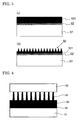
- FIGS. 2A and 2B illustrate a sapphire substrate serving as
a base for the group III nitride semiconductor and AlN buffer layer
formed on the surface of the sapphire substrate, respectively,
both figures showing the procedure of forming nano-pillars;
- FIGS. 3C and 3D illustrate a GaN layer serving as the group
III nitride semiconductor and formed on the surface of the buffer
layer and nano-pillars formed on the surface of the GaN layer,
respectively, both figures showing the procedure of forming
nano-pillars;
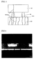
- FIG. 4 is a sectional view of the nano-pillars on which the
group III nitride semiconductor is deposited;
- FIG. 5 is a typical sectional view of the nano-pillars on
which the group III nitride semiconductor is deposited, showing
crystal transition defects (lattice defects);
- FIG. 6 is an electron microscope photograph showing a section
of crystal structure of an etched surface after the group III nitride
semiconductor has been etched by the method described in
embodiment 1;
- FIG. 7 is an electron microscope photograph showing a section
of crystal structure of an etched surface after the group III nitride
semiconductor has been etched by the method described in
embodiment 1, the crystal structure being viewed from obliquely
upward;
- FIG. 8 is a sectional view showing nano-pillars being cut
with a diamond cutter;
- FIG. 9 is a sectional view showing nano-pillars with masks
being applied at predetermined positions;
- FIG. 10 is a sectional view showing an example of a light
detecting device structure in which nano-pillars are provided
on the group III nitride semiconductor;
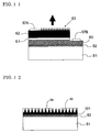
- FIG. 11 is a sectional view showing an example of a light
emitting device (LED) structure in which nano-pillars are provided
on the group III nitride semiconductor;
- FIG. 12 is a sectional view of the group III nitride
semiconductor in the case where the nano-pillars are filled with
a filling substance such as SiO2;
- FIG. 13 is a graph showing the reflectance of the group III
nitride semiconductor film provided with nano-pillars, wherein
the axis of abscissas denotes the wavelength (nm) and the axis
of ordinates denotes the reflectance, and the broken line
represents the reflectance of a conventional group III nitride
semiconductor film and the solid line represents the reflectance
of the group III nitride semiconductor film provided with the
nano-pillars; and
- FIG. 14 is a graph showing the transmittance of the group
III nitride semiconductor provided with nano-pillars, wherein the
axis of abscissas denotes the wavelength (nm) and the axis of
ordinates denotes the transmittance, and the broken line
represents the transmittance of a conventional group III nitride
semiconductor film and the solid line represents the transmittance
of the group III nitride semiconductor film provided with the
nano-pillars.
-
-
In the figures, reference symbol 1 designates an etching
chamber, 2 a high-frequency power supply, 3 an exhaust pipe, 4a
and 4b gas supply pipes, 11 and 12 electrodes, 101 GaN (group
III nitride semiconductor film) and 56 a quartz substrate.
BEST MODE FOR CARRYING OUT THE INVENTION
-
Embodiments of the present invention will now be described
in detail with reference to the drawings. However, the present
invention should not be limited by the following embodiments but
may be changed into various modes without departing from the
essence of the present invention. Furthermore, the technical
scope of the present invention should cover a scope of equality.
1. Best mode for carrying out the first invention:
-
The best mode for carrying out the first invention (that
is, a method of fabricating a group III nitride semiconductor film
including 1 ○a nano-pillar fabricating step and 2 ○a depositing
step) will be described.
<Nano-pillar fabricating step>
-
FIG. 1 is a sectional view of an example of dry etching
apparatus which can be used in the practice of the present invention.
The apparatus includes an etching chamber 1, a high-frequency
power supply 2, an exhaust apparatus and a plasma generating gas
supply apparatus.
-
More specifically, a pair of positive and negative parallel
flat plate-shaped electrodes 11 and 12 are installed so as to
be opposed to each other in the etching chamber 1 made of stainless
steel 1, for example. Of both electrodes, the anode 11 is
maintained at an earth potential whereas a high-frequency power
is applied to the cathode 12. The cathode 12 is beaten by plasma
gas hard such that the temperature thereof is increased.
Accordingly, the cathode 12 has a hollow interior structure so
that cooling water is allowed to flow through the rear side thereof
in order to cool the cathode. A high-frequency power supply 2
of 13.56 MHz is connected via a matching box 22 to the cathode
12, so that plasma is controlled.
-
The exhaust pipe 3 is provided in the etching chamber 1.
An exhauster (not shown) including a combination of a dry pump,
turbo pump and the like is connected to the exhaust pipe 3. The
exhauster is driven so that the interior of the etching chamber
1 is evacuated, whereby pressure in the etching chamber is reduced
to or below 10-4 Pa. The pressure in the etching chamber 1 is
adjusted by a pressure adjusting valve 33 provided in the middle
of the exhaust pipe 3, for example, so that the interior of the
etching chamber is maintained in a predetermined range of vacuum.
-
The etching chamber 1 is provided with gas conduits 4a and
4b introducing plasma generating gases respectively therein. The
other ends of the gas conduits 4a and 4b are connected to external
plasma generating gas sources (not shown) respectively. More
specifically, the etching chamber 1 is provided with the first
gas conduit 4a introducing an etching gas (chlorine gas, for
example) therein and the second gas conduit 4b introducing another
gas (mixed with the first gas for dry etching, if necessary).
Flow rates of the gases are controlled by a massflow controllers
44a and 44b provided across the gas conduits 4a and 4b respectively.
The gas conduit 4b is eliminated or closed when only the first
gas is introduced into the etching chamber 1 as the plasma
generating gas.
-
An operation for etching the group III nitride semiconductor
film using the foregoing etching apparatus 1 (a nano-pillar
fabricating step) will now be described. In the following example,
a step of fabricating nano-pillars on the surface of a GaN layer
is exemplified. However, the technical scope of the present
invention should not be limited to this but covers methods of
fabricating nano-pillars on the surfaces of group III nitride
semiconductor films represented by formula, AlxGayIn1-x-yN (0≤x≤1,
0≤y≤1 and 0≤x+y≤1).
-
Firstly, the structure of the group III nitride semiconductor
film will be described with reference to FIGS. 2A, 2B and 3. The
group III nitride semiconductor film is provided on an upper side
of a buffer layer 52 which is further provided on an upper side
of a sapphire substrate 51, for example, as shown in FIGS. 2A
and 2B. AlN having a thickness of about 20 nm can be used as
the buffer layer 52.
-
A group III nitride semiconductor film 101 (for example, GaN
can be used) is formed on the upper side of the buffer layer 52,
for example, by an MOVPE method (FIG. 3C).
-
In order that the sample 55 having such a structure (meaning
an overall substance including the buffer layer 52 on the surface
of the sapphire substrate 51 and the semiconductor film 101) may
be etched, a solid quartz substrate 56 is placed on the upper
side of each cathode 12 and a wafer of the sample 55 is placed
on or around the quartz substrate. When the sample 55 is placed
on the upper side of the quartz substrate 56, a section of the
quartz substrate 56 is rendered larger than a section of the sample
55 so that the quartz substrate is exposed to the etching gas.
-
The exhauster is then driven so that the etching chamber
1 is exhausted so that the interior pressure is in the order of
10-4 Pa. After the degree of vacuum has become stable, the chlorine
gas is introduced from gas conduit 4a into the interior of the
etching chamber 1 while the flow rate is controlled by the massflow
controller 44a so that a predetermined flow rate is achieved.
In this case, at the same time, the etching chamber 1 is exhausted
by the exhauster and the pressure adjusting valve 33 is adjusted
so that the internal pressure of the etching chamber 1 becomes
a predetermined pressure. Chlorine gas plasma is generated
between both electrodes 11 and 12 when voltage from the
high-frequency power supply 2 is applied via the matching box
22 after the internal pressure of the etching chamber 1 has been
stabilized.
-
The chlorine gas sputters and etches the group III nitride
semiconductor film 101 of the sample 55 while etching the quartz
substrate 56 (the nano-pillar fabricating step). Nano-pillars
50 are thus formed on the surface of the group III nitride
semiconductor film 101 by the etching, as shown in FIG. 8D. Each
nano-pillar 50 has a diameter ranging from about 10 nm to about
200 nm. A space between each nano-pillar 50 and another
nano-pillar 50 adjacent thereto is about 100 nm on the average.
The diameter and space of the nano-pillars 50 can be changed
suitably according the conditions of the etching. A mask in the
order of nanometer is required when an ordinary lithography is
used for formation of the above-described nano-pillars.
Furthermore, a wavelength in the order of nanometer is also
necessary for light used in the exposure. Consequently, a method
using the lithography cannot currently be realized.
-
When the nano-pillars 50 have thus been fabricated, most
of lattice defects 101A present in the lower layer of group III
nitride semiconductor 101 are interrupted from proximal ends of
the nano-pillars 50 to the middle portions, as shown in FIG. 5.
Consequently, the lattice defects are prevented from being taken
over to upper portions of the nano-pillars (that is, portions
serving as a footing for a group III nitride semiconductor film
53 serving as an upper layer). Accordingly, very few lattice
defects 101A are present on the group III nitride semiconductor
53 (the upper layer) deposited on the upper faces of the
nano-pillars 50.
<Depositing step>
-
The new group III nitride semiconductor 53 is then deposited
on the upper sides of the nano-pillars 50 as shown in FIG. 4 (the
depositing step). The depositing method includes the MOVPE
method, HVPE method, MBE method, as described above.
-
When the new group III nitride semiconductor 53 (the upper
layer) has been obtained, the semiconductor is cut between the
upper layer 53 and the nano-pillars 50, whereby the simple upper
layer 53 is obtained. As a method of cutting the upper layer
from the nano-pillars 50, for example, a diamond cutter 200 as
shown in FIG. 8 may be used. Further another group III nitride
semiconductor 53 may be deposited on the upper side of the simple
upper layer 53 serving as a substrate.
2. Best mode for carrying out the third invention:
-
A best mode for carrying out the third invention will now
be described.
(1) Method of fabricating a light detecting device:
-
A light detecting device has such a structure that the buffer
layer 52 is laminated on the upper side of the sapphire substrate
51 and the GaN layer 101 provided with the nano-pillars 50 is
laminated on the buffer layer as shown in FIG. 10.
-
3 ○ the nano-pillar fabricating step can be carried out in
the same manner as <the nano-pillar fabricating step> in "1. Best
mode for carrying out the first invention." Accordingly, the
description will be eliminated so that repetition is avoided.
-
In fabricating the nano-pillars 50, etching may be carried
out with suitable masks 60 (SiO2, for example) being applied,
whereby a group III nitride semiconductor film with a predetermined
pattern on its surface can be fabricated as shown in FIG. 9.
-
Furthermore, electrodes 57 are formed at predetermined
positions where no nano-pillars 50 have been fabricated by
application of masks, whereby a light detecting device as shown
in FIG. 10 can be made.
(2) Process for fabricating a light-emitting device:
-
A light-emitting device can be constructed as shown in FIG.
11. The light-emitting device as shown in FIG. 11 comprises a
group III nitride semiconductor film formed by laminating an n-GaN
layer 60 (a first semiconductor layer) , an InGaN layer 61 (a second
semiconductor layer 61 and serving as light-emitting layer) and
a p-GaN layer 62 (a third semiconductor layer) all laminated on
a substrate provided with the buffer layer 52 provided on the
upper side of the sapphire substrate 51, for example, by MOVPE
method, sequentially in this order. In the aforesaid structure,
the second semiconductor layer is sandwiched between the first
and second semiconductor layers. In order that the
light-emitting device may perform a desired operation, it is
preferable that selection is made so that the second semiconductor
layer is made of such a substance that the band gap energy of
the second semiconductor layer is smaller than the band gap energy
of the first semiconductor layer and the band gap energy of the
third semiconductor layer. The first semiconductor layer may
have a thickness of about several hundreds to several thousands
nm. The second semiconductor layer may have a thickness of about
several nm to about 60 nm. The third semiconductor layer may
have a thickness of about several nm to one hundrednm. Furthermore,
the paired positive and negative electrodes 57A and 57B are
provided on the p-GaN layer 62 and n-GaN layer 60 respectively.
-
A procedure for fabricating nano-pillars on the outermost
layer will be described. The n-GaN layer 60, InGaN layer 61 and
p-GaN layer 62 are grown via the buffer layer 52 on the upper
side of the sapphire <0001> substrate, for example, by the MOVPE
method. In this case, each of the n-GaN and p- GaN layers 60 and
62 has a thickness of about 300 nm and the InGaN layer 61 has
a thickness of about 20 nm. Furthermore, SiO2 is deposited on
the upper side, for example, by the RF sputtering, so as to have
a thickness of about 300 nm and a line of 5 µm wide and space
pattern are fabricated in the <1100> direction by the ordinary
photolithography technique, whereby an etching sample 55 is made.
The same operation is carried out as in the <nano-pillar
fabricating step> in "1. Best mode for carrying out the first
invention" except for use of the sample 55, whereupon nano-pillars
63 can be fabricated on the surface of p-GaN layer 62.
-
A pair of positive and negative electrodes 57A and 57B are
formed on the group III nitride semiconductor film thus fabricated.
The positive electrode 57A is formed on the upper side of the
p-GaN layer 62. The negative electrode 57B is formed on the surface
of the n-GaN layer 60 after a depression has been formed by the
etching so as to extend through the p-GaN layer 62 and InGaN layer
61 and reach the n-GaN layer 60.
-
After fabrication of the nano-pillars 50, spaces between
the nano-pillars 50 may be filled with a suitable filling material
58 (for example, ITO (indium tin oxide) , Al2O3, SiO2 or the like)
as shown in FIG. 12 (the filling step). It is preferable that
a chemical etching is carried out in order that the etching
retarding substance on the nano-pillar surfaces maybe eliminated
so that the elimination contributes to smooth formation of a
filling layer. As a method of filling the nano-pillars 50 is
exemplified a metal organic vapor phase epitaxy method (MOVPE) ,
a hydride VPE method (HVPE), a molecular beam epitaxy method (MBE)
or the like.
<Embodiments>
(1) Nano-pillar fabricating step:
-
GaN (gallium nitride) was grown on a sapphire <0001>
substrate by the MOVPE method so as to have a thickness of 2 µm
to 3 µm and was used as the group III nitride semiconductor (the
lower layer).
-
SiO2 was deposited on the upper side of GaN, for example,
by the RF sputtering, so as to have a thickness of about 300 nm
and a line of 5 µm wide and space pattern were fabricated in the
<1100> direction by the ordinary photolithography technique,
whereby an etching sample 55 was made.
-
The quartz substrate 56 was installed on a stage of the etching
chamber 1. The etching sample 55 was placed around the quartz
substrate 56 and on the upper side of the quartz substrate.
-
Thereafter, the etching chamber 1 was exhaustedby the vacuum
pump so that the internal pressure was reduced to 5×10⁻⁴ Pa. After
the degree of vacuum had become stable, the chlorine gas was
introduced from gas conduit 4a into the interior of the etching
chamber 1 while the flow rate was controlled by the massflow
controller 44a so that a flow rate of 30 ml/min was achieved.
At the same time, the etching chamber 1 was exhausted by the vacuum
pump and the pressure adjusting valve 33 was adjusted so that
pressure reduction by 6 Pa was achieved.
-
After stabilized degree of vacuum in the etching chamber
1 had been confirmed, voltage from the high-frequency power supply
2 was applied so that plasma was generated between both electrodes
11 and 12. The dry etching was carried out for about four minutes
under the condition of 100 W (an area of 177 cm2).
-
The sample 55 was taken out of the etching chamber 1 after
the dry etching and the etched side was observed by a scanning
electron microscope (SEM). FIGS. 6 and 7 are views showing
photographs of etched side structure of GaN taken by SEM during
the observation. According to the embodiment, a chlorine ion
in the plasma strikes the quartz substrate around GaN, whereupon
SiO2 moves out into the plasma by the sputtering effect. It is
supposed that part of SiO2 is ionized thereby to re-adhere to
the negative biased GaN film. Since SiO2 has an etching rate
of one-tenth to one-twentieth relative to the chlorine gas plasma,
which value is lower as compared with GaN, SiO2 serves as a
micro-mask, whereupon a micro rugged structure is formed on the
surface of the sample 55. Since the electric field is higher
in a slightly convex portion than in the concave portion, the
subsequently ionized SiO2 will adhere to the convex portion with
a higher probability. Thus, it is supposed that re-adherence
of the etching retarding substance and etching by an etching gas
plasma repeatedly progress, whereby the nano-pillars are
fabricated. The nano-pillar had a thickness of about several
tends nm to several hundreds nm and a height of about 500 nm.
Furthermore, the nano-pillars had a distribution density of
106/cm2 to 1012/cm2. It became clear that the height of the
nano-pillar depended largely upon the etching time.
(2) Depositing step:
-
Another GaN (an upper layer) was able to be grown on the
upper side of GaN of the nano-pillars thus fabricated, for example,
by the MOCVD method (see FIG. 4). As the conditions in this case,
trimethyl gallium (TMG) was caused to flow at 48 µmol/min and
NH3 was caused to flow at µmol/min. The temperature was 1000°C
and pressure was 300 Torr. Under these conditions, the growth
of GaN by about 3 µm to 4 µm per hour was confirmed. GaN of the
upper layer had a film thickness of about 3 µm.
(3) Separating step:
-
The upper layer was cut from the nano-pillars using a diamond
cutter so as to be separated from the nano-pillars. FIG. 8
illustrates a manner of separating the upper layer 53 by pressing
a rotary diamond cutter along the nano-pillars 50. The rear side
(on which the nano-pillars were present) of the upper layer 53
thus obtained as a single body was ground and flattened. Thus,
the GaN semiconductor film having fewer lattice defects and a
larger film thickness was able to be obtained. Differing from
the prior art (that is, the GaN layer provided on the upper side
of the non-conductive sapphire substrate), the upper layer 5 is
a monolayer of GaN and no other substrate is present at the rear
side thereof.
-
When the aforesaid GaN film is used as a substrate,
crystallinity suitable for a group III nitride semiconductor layer
grown on the upper side thereof is obtained. Furthermore, this
substrate can be afforded the electrical conductivity, differing
from the conventional sapphire substrate. Accordingly,
electrodes can be formed both sides of a group III nitride
semiconductor element. Consequently, the number of steps in the
fabrication of semiconductor element can be reduced and a cost
reduction can be achieved in the present invention as compared
with the conventional semiconductor elements.
Embodiment 2: Characteristic evaluation of the group III nitride
semiconductor film provided with nano-pillars:
-
Characteristics of the foregoing group III nitride
semiconductor film provided with nano-pillars were evaluated.
FIG. 12 is a graph showing the relationship between the wavelength
and reflectance and FIG. 13 is a graph showing the relationship
between the wavelength and transmittance.
-
Regarding the reflectance and transmittance, data of GaN
with nano-pillars (solid line) and GaN without nano-pillars
(broken line) were compared with each other. In each graph, a
cyclic oscillation is due to light interference by the GaN film.
In a range of wavelength shorter than 800 nm, both reflectance
and transmittance are effective (that is, the reflectance is
reduced and the transmittance is improved). Regarding the
nano-pillars, the reflectance is approximate to zero in a range
of wavelength shorter than about 360 nm corresponding to a band
gap of GaN. In a wavelength range not more than the band gap,
the transmittance necessarily becomes zero since light is absorbed
into GaN (FIG. 13). However, since the transmittance is improved
in a wavelength range longer than the band gap, it is supposed
that light is absorbed into the GaN crystal efficiently without
being reflected in the case of the nano-pillars in a wavelength
range not more than the band gap.