EP1422617A2 - Coprocessor architecture based on a split-instruction transaction model - Google Patents
Coprocessor architecture based on a split-instruction transaction model Download PDFInfo
- Publication number
- EP1422617A2 EP1422617A2 EP03257264A EP03257264A EP1422617A2 EP 1422617 A2 EP1422617 A2 EP 1422617A2 EP 03257264 A EP03257264 A EP 03257264A EP 03257264 A EP03257264 A EP 03257264A EP 1422617 A2 EP1422617 A2 EP 1422617A2
- Authority
- EP
- European Patent Office
- Prior art keywords
- instruction
- extension
- extension unit
- result
- processor
- Prior art date
- Legal status (The legal status is an assumption and is not a legal conclusion. Google has not performed a legal analysis and makes no representation as to the accuracy of the status listed.)
- Withdrawn
Links
Images


Classifications
-
- G—PHYSICS
- G06—COMPUTING OR CALCULATING; COUNTING
- G06F—ELECTRIC DIGITAL DATA PROCESSING
- G06F9/00—Arrangements for program control, e.g. control units
- G06F9/06—Arrangements for program control, e.g. control units using stored programs, i.e. using an internal store of processing equipment to receive or retain programs
- G06F9/30—Arrangements for executing machine instructions, e.g. instruction decode
- G06F9/38—Concurrent instruction execution, e.g. pipeline or look ahead
- G06F9/3885—Concurrent instruction execution, e.g. pipeline or look ahead using a plurality of independent parallel functional units
-
- G—PHYSICS
- G06—COMPUTING OR CALCULATING; COUNTING
- G06F—ELECTRIC DIGITAL DATA PROCESSING
- G06F9/00—Arrangements for program control, e.g. control units
- G06F9/06—Arrangements for program control, e.g. control units using stored programs, i.e. using an internal store of processing equipment to receive or retain programs
- G06F9/30—Arrangements for executing machine instructions, e.g. instruction decode
- G06F9/30003—Arrangements for executing specific machine instructions
- G06F9/3004—Arrangements for executing specific machine instructions to perform operations on memory
- G06F9/30043—LOAD or STORE instructions; Clear instruction
-
- G—PHYSICS
- G06—COMPUTING OR CALCULATING; COUNTING
- G06F—ELECTRIC DIGITAL DATA PROCESSING
- G06F9/00—Arrangements for program control, e.g. control units
- G06F9/06—Arrangements for program control, e.g. control units using stored programs, i.e. using an internal store of processing equipment to receive or retain programs
- G06F9/30—Arrangements for executing machine instructions, e.g. instruction decode
- G06F9/30003—Arrangements for executing specific machine instructions
- G06F9/30072—Arrangements for executing specific machine instructions to perform conditional operations, e.g. using predicates or guards
Definitions
- the present invention is directed, in general, to processor instruction set architectures (ISAs) and, more specifically, to extending or altering processor instruction set architectures.
- ISAs processor instruction set architectures
- Processor instruction set requirements generally evolve with changing application domains.
- digital signal processing applications can be made to perform better with special instructions.
- the particular instructions needed to achieve such performance improvement typically change over time.
- a primary object of the present invention to provide, for use in a processor architecture, an electrical interface for coupling the processor core to one or more coprocessor (core extension) units executing computational (user-defined) instructions, with a split-instruction transaction model employed to provide an instruction and the instruction's operands to the extension unit and to retrieve results from the extension unit.
- the generic core-extension instructions allow for new computational instructions to be introduced, together with the capability to send data to an extension unit and/or retrieve a result from the extension unit, without regeneration of the processor architecture.
- Support is included for multiple extension units and/or multiple execution pipelines within each extension unit, multi-cycle execution latencies and different execution latencies between or within extension units, extension unit instruction predicates, processor core stalls and result save/restore on interrupt.
- FIGURES 1 through 5 discussed below, and the various embodiments used to describe the principles of the present invention in this patent document are by way of illustration only and should not be construed in any way to limit the scope of the invention. Those skilled in the art will understand that the principles of the present invention may be implemented in any suitably arranged device.
- FIGURE 1 depicts a processor architecture including a split transaction model coprocessor extension interface according to one embodiment of the present invention.
- the present invention defines a flexible alternative for a high-performance digital signal processor that includes a customizable coprocessor extension architecture with a well-defined coprocessor interface supporting multiple coprocessors. This architecture allows for easy integration of the coprocessor with a core hard macro for SOC (System On Chip) designs.
- SOC System On Chip
- Processor architecture 100 comprises a core 101 including a program memory controller PMC with program memory (not explicitly shown), a control unit CU, two data unit pipelines DU-0 and DU-1 working with a data register file DRF, a data memory banks X and Y.
- Each data unit includes a data operand fetch pipeline stage (DOF) where source operands Rn, Rp are retrievd (fetched) from the DRF; two execute pipeline stages EX1 and EX2 where standard core instructions execute; and a write-back (WB) stage where instruction result Rm is written into the DRF.
- DOF data operand fetch pipeline stage
- EX1 and EX2 where standard core instructions execute
- WB write-back
- Coupled to one data unit pipeline DU-0 is a coprocessor extension electrical interface 102 comprising a five bit extension strobe bus x_strobe, a twenty-nine bit extension instruction bus x_inst, a thirty-two bit coprocessor extension first operand bus x_opa, a thirty-two bit coprocessor extension second operand bus x_opb, and a forty bit coprocessor extension result bus x_result.
- the extension interface 102 couples the core 101 to one or more coprocessor extension units 103a-103d, each optionally including a first-in, first-out (FIFO) output buffer 104a-104d.
- the coprocessor extension units 103a-103d are addressed utilizing a two bit identifier, which implies support for up-to four coprocessor extension units.
- the present invention may be readily limited or extended to fewer or more coprocessor extension units.
- the x_strobe signals comprise information from different pipeline stages of the core 101, including a one bit coprocessor extension instruction valid x_valid signal, a one bit signal x_schedule indicating that the valid coprocessor extension instruction is scheduled and is in the execute stage 1 (EX1) pipe-stage, a two bit coprocessor extension instruction predicate value signal x_guard, and a one bit write back signal x_wb indicating that the coprocessor extension instruction is expected to produce a result.
- the processor core 101 may potentially stall, in which case the x_schedule signal would be inactive in the following cycle. Therefore, until x_schedule becomes active, the coprocessor extension should continue to decode the x_inst issued in the prior cycle.
- FIGURES 2A through 2C are timing diagrams illustrating the operation of split transaction execution with pipelined and non-pipelined operation and with and without a result queue for split transaction coprocessor extensions according to various embodiments of the present invention.
- the coprocessor extension includes an application specific function having a latency of L cycles and a throughput of T cycles used in pipelined fashion.
- the coprocessor extension instructions follow a split-transaction model where a minimum of two coprocessor extension instructions are required to execute an operation in the coprocessor and retrieve the operation result from the coprocessor.
- a single transaction model needs only a single coprocessor instruction to initiate the operation and provide an internal core destination. This model may also be employed in the present invention in the case where the operation result is stored inside the coprocessor, either as an internal state or in a coprocessor register file.
- the first core-extension instruction provides the operands and operation to the coprocessor and the second core-extension instruction retrieves the result generated by the previous instruction (and optionally also sends another operation with associated operands, to be explained later).
- This split-transaction model allows user-defined latencies of coprocessor extension functions, and takes a minimum of L cycles.
- the first core-extension instruction that sends a user-defined operation and operand(s) to a coprocessor extension unit 103a-103d is represented in the instruction set architecture (ISA) for the processor core 101 as: where xspc is an e x tension s pe c ific instruction field that specifies the (user-defined) coprocessor operation.
- ISA instruction set architecture
- the second core-extension instruction that sends an operation and retrieves a result is represented in the core ISA as:
- the upper portion 201a of FIGURE 2A illustrates the operations within the processor core 101, while the lower (italicized) portion 201b illustrates the corresponding operations within the coprocessor extension interface 102.
- the corresponding assembly code for the instruction sequence illustrated in FIGURE 2A is shown below in TABLE II: PC [31:0] (GP32 Mode) DU Instruction Slot 1 Slot 0 0x100 DU-OP Gx?
- the coprocessor extension is operated in a pipelined manner, one result may be produced from the coprocessor extension unit every cycle.
- the definition of the coprocessor extension architecture is limited in this embodiment to issuing only one coprocessor instruction per cycle.
- the coprocessor extension cannot be operated in a pipelined manner for code sequences including an XSD followed by an XLD. Therefore, an instruction of the form send data and load data XSDLD is needed that implies sending the operation and operand(s) to the extension and concurrently loading a result from the extension.
- the coprocessor extension instructions are tagged with an identifier in parentheses indicating the load data instruction XLD that matches with each send data instruction XSD.
- a pair of identifiers in parentheses is used with the first corresponding to the send data part and the second corresponding to the instruction whose result the load data part retrieves (Rm: destination operand register; Rn, Rp: source operand registers).
- FIGURE 2B illustrates pipelining of coprocessor extension operations assuming that the result is retrieved using either the load data instruction XLD or the load data component of the combined instruction XSDLD, if performed optimally.
- the processor core 101 either stalls (the coprocessor is not aware of core stalls) or switches threads due to an interrupt, and is therefore unable to pick up the result in an optimal manner, a clear possibility exists of losing the coprocessor result in the absence of temporary storage for that result.
- a FIFO result queue (RQ) structure 104a-104d is needed for each coprocessor extension unit 103a-103d to hold the spill over, enabling the coprocessor extension pipeline to run independently of the processor core 101 without being influenced by core stall conditions (since the coprocessor extension unit 103a-103d does not stall when the processor core 101 stalls).
- the presence of a result queue implies that the load data instruction (or the load data component of a combined instruction) will always retrieve the result from the bottom of the FIFO structure.
- Extra entries within a FIFO result queue 104a-104d can ease instruction scheduling.
- coprocessor extension units 103a-103d may be connected to the processor core 101, each of which should have a FIFO result queue 104a-104d. Since latency and throughput are parameters of the individual coprocessor extension units 103a-103d and may be different for different coprocessors, the depths of the respective FIFO result queues 104a-104d may also differ.
- a coprocessor extension unit 103a-103d is updated only if the instruction predicate (the predicate status arriving during the data unit execute stage 2 DU-EX2) is true, coprocessor results will be written into the respective FIFO result queue and the FIFO valid counter updated, always irrespective of the predicate state.
- XLD or corresponding instruction components always read from the FIFO result queue and update the FIFO status with regard for the predicate status, which removes timing constraints due to late arrival of the predicate in the DU-EX2 stage.
- Any coprocessor extension unit 203a-203d without a FIFO result queue should include a result register coupled to the coprocessor extension result bus x_result.
- CR0 and CR1 are each assumed to represent either an internal state or register identifiers for a coprocessor-specific register file, while xfn indicates a coprocessor function specified using the #xspc field of the instruction.
- the critical coprocessor pipeline stage in FIGURE 2C is the "Read Internal State & Write Result_Register of Extension.”
- the architecture described above may be implemented in an ST120 processor, available from STMICROELECTRONICS, INC., with four versions of the XSD instruction, identical in encoding and differing only in the primary operation code (opcode) description. Similarly, two versions of the XLD instruction, four versions of the XSDLD instruction, and two versions of the XOP instruction may be implemented.
- the instruction set encoding includes a 2-bit field Ext#[1:0] that allows addressing of up to four coprocessor extension units.
- Xa refers to writing into the FIFO result queue while, on the right hand side, “Xa” refers to reading out of the FIFO result queue.
- ⁇ I> indicates the forms of the instruction (e.g., XSD1, XSD2, XSD3 or XSD4). All coprocessor instructions have an extension specific field xspc with the width, in bits, indicated by the appended number.
- Coprocessor extensions may be one of two types: coprocessors without any internal state or register file--i.e., a pure execution unit with a result queue (RQ) (Type A); and coprocessors with an internal state and/or register file, execution unit(s) and a result queue (Type B).
- RQ result queue
- Type A coprocessors without any internal state or register file--i.e., a pure execution unit with a result queue (RQ) (Type A); and coprocessors with an internal state and/or register file, execution unit(s) and a result queue (Type B).
- RQ refers to the FIFO result queue
- Cn refers to the coprocessor internal state (e.g., internal register)
- x_result refers to the coprocessor result bus connecting to the core.
- Alternatives referencing internal register Cn exist only when the coprocessor has an internal state (Type B).
- the predicate usage is similar to that of the existing ST120, with the XSD operation or component part of XSDLD or XOP instruction executed speculatively and only the part of the XLD component that writes to the DRF being predicated. It is important to note that write to the result queue and reads from the result queue are not predicated, such that Type A coprocessor extensions do not require the predicate from the core.
- XSDLD instructions are broken into two (XSD and XLD) instructions with their respective unique predicates as illustrated in the example given in TABLE VIII: PC Slot 1 Slot 0 Instruction Components XSD XLD 0x100 DU-OP Gx? XSD Rn, Rp, #xspc11 Gx? XSD 0x108 DU-OP Gy? XSD Rn, Rp, #xspc11 Gy? XSD 0x110 DU-OP Gx? XSDLD Rm, Rn, Rp, #xspc7 Gx? XSD Gx? XLD 0x118 DU-OP Gy? XLD Rm, #xspc15 Gy? XLD 0x120 DU-OP Gx? XLD Rm, #xspc15 Gx? XLD
- the FIFO result queue is written and updated irrespective of the predicate status of the instruction, and the FIFO result queue is read and the FIFO result queue pointers are updated on an XLD component irrespective of the predicate status of the instruction.
- the coprocessor extension supplying the operands and extension specific opcode followed at a later time by another instruction retrieving the result of the corresponding earlier instruction should share the same predicate.
- FIGURE 3 illustrates a scheme for handling non-uniform instruction latencies within split transaction coprocessor extension units according to one embodiment of the present invention.
- a coprocessor extension unit 103 may conceivably have several execution units 301, 302 performing different types of instructions each with different execution latency.
- the results of coprocessor instructions must be retrieved in program order. Assuming that two consecutive instructions i1, i2 with latencies L1, L2 are to be sent to the coprocessor (not necessarily in consecutive cycles), and that the execution units 301, 302 performing these instructions write results to the FIFO result queue 104 via a single port 303, two cases are presented:
- the scheduler must be aware of the respective latencies of consecutive (or closely spaced) instructions received for issuance to the same coprocessor extension and, in the case of L2 ⁇ L1, should wait L1-L2 cycles before dispatching the second instruction i2 to the coprocessor extension.
- the scheduler need not wait to dispatch instruction i2 when L2 ⁇ L1.
- the scheduler should apply these rules to optimally use the execution engines within the coprocessor extension.
- FIGURE 4 illustrates one possible mechanism for connecting the result buses of multiple coprocessor extensions within split transaction coprocessor extension units according to one embodiment of the present invention.
- the exemplary embodiment described above allows for up to four different coprocessor extension units, with potentially different instruction latencies. If each extension unit has a FIFO result queue, the scheduling rules of each extension unit need to be respected.
- the coprocessor may start a new calculation and write a new result every cycle to the DRF.
- results produced by the coprocessor cannot be moved into the data unit during draining of the pipeline, and the results would be lost absent temporary storage.
- the FIFO result queue is thus placed between the last pipe stage of the coprocessor and the core data unit to hold these results produced by the coprocessor.
- the programmer must ensure that at any cycle the number of pending results is less than or equal to the FIFO result queue depth so that the FIFO result queue cannot overflow in the event of an interrupt or core stall condition.
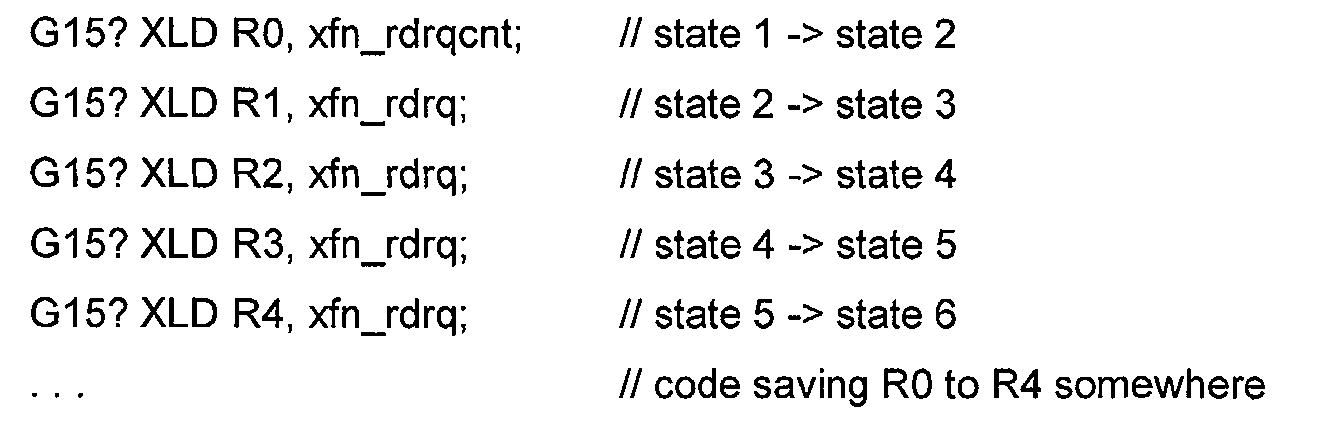
- the number of valid entries in the FIFO result queue is contained within a register FIFO Counter (not shown), with reads and writes to the FIFO result queue conforming to the following rules:
- FIGURE 5 is a timing diagram illustrating operation of an example Galois multiplier split transaction coprocessor extension unit according to one embodiment of the present invention.
- the exemplary Galois multiplier extension (GMX) unit takes two 32-bit operands and produces a 32-bit result performing a Galois multiply on four 8-bit fields.
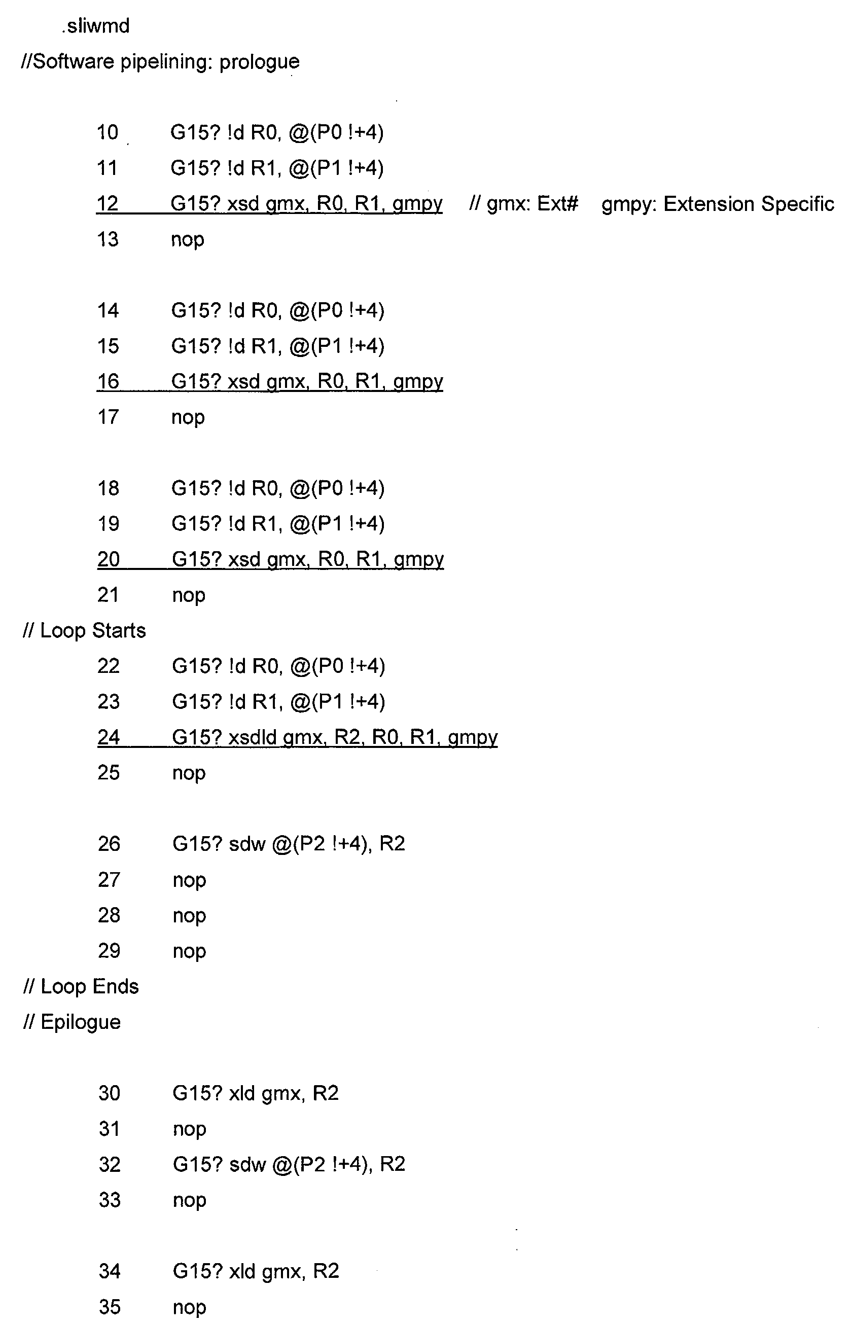
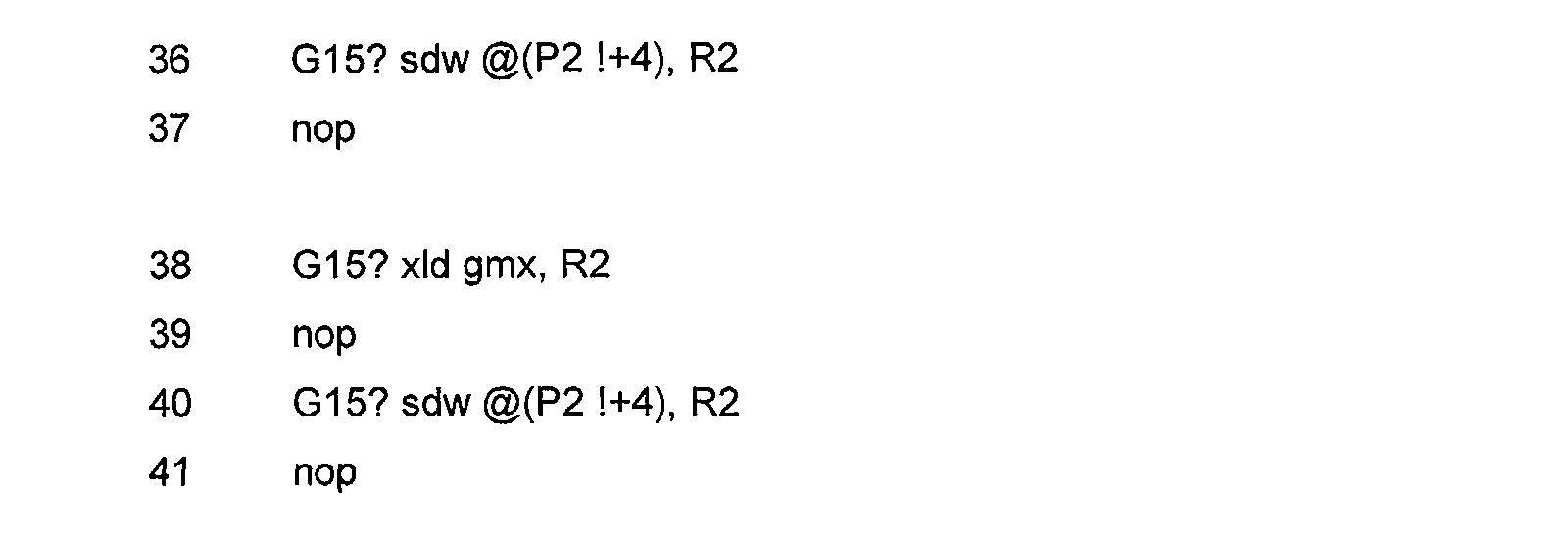
- the extension unit is identified as GMX in the Ext# field, and is assumed to include a fully pipelined, two-cycle extension execution engine followed by a single cycle write to the result queue, such that the latency seen by the program on the core is 3 cycles. With software pipelining, one result can be produced and written to the DRF per cycle after the initial latency, as illustrated in the pseudo-code sequence below:
- the basic model is to read the Galois fields from memory and write two 32-bit data register file (DRF) operands to the extension unit using XSD to prime the pipeline. Once the pipeline is set-up, XSDLD is used to retrieve the result and supply the next two 32-bit DRF operands. Note that in instruction 24 an operation and two operands are supplied and the result retrieved using a single instruction.
- DRF data register file
- FIGURE 5 illustrates operation of the extension when operands must be retrieved from memory and the result of the extension instruction must be stored in memory.
- the numbers within the instructions correspond to the instructions in the pseudo-code above.
- a result is retrieved every other cycle, and the core only allows two memory address unit (AU) operations per cycle while each loop iteration requires three memory accesses (two loads, one store).
- the coprocessor interface has the capability to produce a result every cycle.
- the FIFO result queue needs to be three deep to hold the results before returning them to the core, which becomes important when an interrupt occurs inside this loop or under stalling conditions.
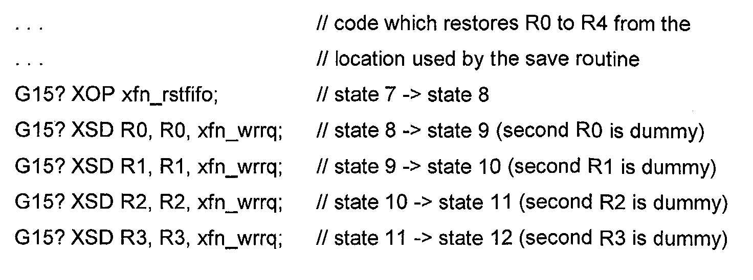
- the interrupt handler should be able to retrieve, store and restore the results from the three-entry deep FIFO in case another thread requires use of this coprocessor.
- a split transaction extension unit provides a flexible alternative for customizing high performance digital signal processors, allowing an execution unit with a special instruction to be added without complete redesign of the architecture.
- the coprocessor architecture is customizable with a well-defined interface supporting multiple coprocessors, allowing for easy integration of the coprocessor with a core hard-macro on a System On Chip (SOC) processor subsystem.
- SOC System On Chip
- the coprocessor architecture is based on a split-instruction transaction model tightly coupled to the core data unit to appear like another data unit.
- the architecture of the present invention accommodates multi-cycle latency extension execution and fully exploits decoupled architectures.
- a scalable FIFO result queue with associated save/restore instruction forms is defined to support efficient pipelining and static scheduling of coprocessor operations, and an additional internal state may be added at will.
- the present invention supports multi-cycle latency execution extensions and generic coprocessor instructions to effectively pipeline multi-cycle execution operations.
- the scalable FIFO result queue removes register pressure and accommodates stalls in the core, allowing the coprocessor extension pipeline to operate independently with respect to the core. Instruction predicates are available to the coprocessor extension.
- the architecture of the exemplary embodiment supports up to four coprocessor extension units and at least two types of connection (OR logic or tri-state) for result buses from the coprocessors. Non-uniform latencies in a coprocessor extension and multi-cycle are supported.
Landscapes
- Engineering & Computer Science (AREA)
- Software Systems (AREA)
- Theoretical Computer Science (AREA)
- Physics & Mathematics (AREA)
- General Engineering & Computer Science (AREA)
- General Physics & Mathematics (AREA)
- Advance Control (AREA)
Abstract
Description
| Signal Name | Width | Type | Pipe Stage | Description |
| x_valid | 1 | Output | DOF | Coprocessor instruction is valid |
| x_inst | 28:0 | Output | DOF | Coprocessor extension instruction [31:7|3:0] |
| x_schedule | 1 | Output | EX1 | Coprocessor instruction that was valid in cycle DOF has entered DU Pipe EX1 stage |
| x_opa | 31:0 | Output | EX1 | First coprocessor operand |
| x_opb | 31:0 | Output | EX1 | Second |
| x_wb | ||||
| 1 | Output | EX1 | Coprocessor instruction with XLD component is in | |
| x_except | ||||
| 1 | Input | EX1 | Exception status driven by | |
| x_guard | ||||
| 2 | Output | EX2 | Predicate Gx, (Gx_16) state | |
| x_result | 39:0 | Input | EX2 | Coprocessor result bus |


| PC [31:0] (GP32 Mode) | | |
| Slot | ||
| 1 | | |
| 0x100 | DU-OP | Gx? XSD Rn, Rp, #xspc11 |
| 0x108 | DU-OP | DU-OP |
| 0x110 | DU-OP | DU-OP |
| 0x118 | DU-OP | Gx? XLD Rm, #xspc15 |
| 0x120 | DU-OP | Gy? XSD Rn, Rp, #xspc11 |
| 0x128 | DU-OP | DU-OP |
| 0x130 | DU-OP | DU-OP |
| 0x138 | DU-OP | Gy? XLD Rm, #xspc15 |
| PC [31:0] (GP32 Mode) | | |
| Slot | ||
| 1 | | |
| 0x100 | DU-OP | XSD Rn, Rp, #xspc11 (1) |
| 0x108 | DU-OP | XSD Rn, Rp, #xspc11 (2) |
| 0x110 | DU-OP | XSD Rn, Rp, #xspc11 (3) |
| 0x118 | DU-OP | XSDLD Rm, Rn, Rp #xspc7 (4)(1) |
| 0x120 | DU-OP | XSDLD Rm, Rn, Rp #xspc7 (5)(2) |
| 0x128 | DU-OP | XLD Rm, #xspc15 (3) |
| 0x130 | DU-OP | XLD Rm, #xspc15 (4) |
| 0x138 | DU-OP | XLD Rm, #xspc15 (5) |
In the case of the send data and load data instruction XSDLD, a pair of identifiers in parentheses is used with the first corresponding to the send data part and the second corresponding to the instruction whose result the load data part retrieves (Rm: destination operand register; Rn, Rp: source operand registers).
| PC [31:0] (GP32 Mode) | | ||
| Slot | |||
| 1 | | Comments | |
| 0x100 | DU-OP | XSD CR0, Rn, Rp, xfn (1) | CR0=xfn(Rn, Rp) |
| 0x108 | DU-OP | XSD CR1, Rn, Rp, xfn (2) | CR1=xfn(Rn, Rp) |
| 0x110 | DU-OP | XLD Rm, CR0, xfn_nop (3) | Rm=CR0 |
| 0x118 | DU-OP | XLD Rm, CR1, xfn_nop (4) | Rm=CR1 |
XOP #xspc19
where the instruction includes nineteen user-defined bits. This format enables the coprocessor extension unit to perform an internal operation using either an immediate or internal state and to update an internal state (although internal state updating is not limited to XOP).
| [31:28] | [27:24] | [23:22] | [21] | [20:17] | [16:11] | [10:7] | [6:0] |
| Ga | xspc [10:7] | Ext#[1:0] | xspc [6] | Rb | xspc [5:0] | Rc | XSD (4 opcodes) |
| Source | Source | ||||||
| Ga | Ra | Ext#[1:0] | xspc [6] | Rb | xspc [5:0] | Rc | XSDLD (4 opcodes) |
| Dest. | Source | Source | |||||
| Ga | Ra | Ext#[1:0] | Xpsc [14:0] | XLD (2 opcodes) | |||
| Dest. | |||||||
| Ga | xspc [10:7] | Ext#[1:0] | Xpsc [14:0] | XOP (2 opcodes) |
| Mnemonic Syntax | GP32 Semantics | xfn Field Width |
| Gx? XSD<I>a, Rn, Rp, #xspc11 | Gx? [Xa=]xfn (Rn,Rp) | xspc[10:0] |
| Gx? XSDLD<i>a, Rm, Rn, Rp, #xspc7 | Gx? Rm=Xa ∥ xfn(Rn,Rp) | xspc[6:0] |
| Gx? XLD<I>a, Rm, #xspc15 | Gx? Rm=Xa, xfn | xspc[14:0] |
| Gx? XOP<I>a, #xspc19 | Gx? [Xa=]xfn | xspc[18:0] |
| Instruction | Coprocessor Semantics | Comment |
| Gx? XSD Rn, Rp, #xspc11 | [RQ=]xfn(Rn,Rp) | Write to RQ is not predicated |
| Gx? [Cn=]xfn(Rn,Rp) | In case of internal register, Cn is written to only if Gx is true | |
| Gx? XLD Rm, #xspc15 | x_result=RQ | RQ is always read from |
| Gx? Rm=x_result | Rm written to if Gx is true | |
| Gx? xfn() | Guarded internal operation | |
| Gx? XSDLD Rm, Rn, Rp, #xspc7 | [RQ=]xfn(Rn,Rp) | Write to RQ is not predicated |
| Gx? [Cn=] xfn(Rn,Rp) | In case of internal register, Cn is written to only if Gx is true | |
| x_result=RQ | RQ is read from always | |
| Gx? Rm=x_result | Rm written to if Gx is true | |
| Gx? XOP #xspc19 | [RQ=]xfn() | Write to RQ is not predicated |
| Gx? [Cn=]xfn() | In case of internal register, Cn is written to only if Gx is true |
| | Slot | 1 | | Instruction Components |
| XSD | XLD | |||
| 0x100 | DU-OP | Gx? XSD Rn, Rp, #xspc11 | Gx? XSD | |
| 0x108 | DU-OP | Gy? XSD Rn, Rp, #xspc11 | Gy? XSD | |
| 0x110 | DU-OP | Gx? XSDLD Rm, Rn, Rp, #xspc7 | Gx? XSD | Gx? XLD |
| 0x118 | DU-OP | Gy? XLD Rm, #xspc15 | Gy? XLD | |
| 0x120 | DU-OP | Gx? XLD Rm, #xspc15 | Gx? XLD |
- when read, an empty FIFO result queue returns the last valid result already returned and the FIFO Counter remains unchanged at zero;
- when read, a non-empty FIFO result queue returns the oldest entry, then drops that entry and decrements FIFO Counter;
- when read and simultaneously written, an empty FIFO result queue returns back the last valid result previously returned, creates a new entry with the written data, and increments the FIFO Counter;
- when read and simultaneously written, a non-empty FIFO result queue returns the oldest result, drops that result, creates a new entry with the written data, and leaves the FIFO Counter unchanged;
- when read and simultaneously written, a full FIFO result queue works as just explained with the behavior guaranteed by the FIFO result queue microarchitecture or by implementing one more entry than required by the FIFO result queue theoretical size;
- when written, an empty FIFO result queue creates a new entry with the written data and increments the FIFO Counter (from 0 to 1);
- when written, a non-empty FIFO result queue creates a new entry with the written data and increments the FIFO Counter (from 0 to 1); and
- when written, a full FIFO result queue has undefined behavior.
| Coprocessor Instruction | Description |
| XLD Rm, xfn_rdrqcnt | • Move the FIFO into the DU register Rm and copy the FIFO Counter value into the FIFO. • If the FIFO Counter is 0, it is incremented; else it remains unchanged. |
| XLD Rm, xfn_rdrq | • Move the FIFO into the DU register Rm. • If the FIFO Counter is 0, it remains unchanged; else it is decremented. |
| XOP xfn_rstfifo | • Reset FIFO Counter |
| XSD Rn, Rp, xfn_wrrq | Dedicated to 32-bit FIFO: • Move Rn[31:0] into the 32-bit FIFO (Rp[31:0] is lost). • FIFO Counter is incremented by 1. |
| Dedicated to 40-bit FIFO: • Move the concatenation of Rp[23:16] and Rn[31:0] into the 40-bit FIFO (Rp part in 8 MSB and Rn part in 32 LSB). • FIFO Counter is incremented by 1. | |
| XSD Rn, xfn_wrrqcnt | • Move Rn[31:0] into the 32-bit FIFO Counter. |
| Note that the FIFO result queue width may be either 32 or 40 bits in the exemplary embodiment. |


Claims (24)
- A processor extension mechanism comprising:a processor core;an electrical interface capable of coupling the processor core to an extension unit for performing at least one computational operation on one or more operands, the electrical interface including connections to one or more instruction and operand buses and a result bus; anda controller capable of issuing a first instruction on the electrical interface to initiate execution of a computational operation within an extension unit and issuing a second instruction on the electrical interface to retrieve a result of the computational operation.
- The mechanism according to claim 1, wherein the controller comprises a data unit within the processor core.
- The mechanism according to claim 1 or 2, wherein the controller supports:an instruction for sending an operation and data to an extension unit,an instruction for sending an operation to and loading data from an extension unit,an instruction for concurrently sending and operation and data to an extension unit and loading data from that extension unit, andan instruction for sending an operation to an extension unit.
- The mechanism according to any preceding claim, wherein the electrical interface is capable of coupling the processor core to a plurality of extension units each performing at least one computational operation on one or more operands.
- The mechanism according to any preceding claim, further comprising:an extension unit capable of executing two or more instructions each having different execution latencies.
- The mechanism according to claim 5, further comprising:a result queue coupled between the extension unit and the controller and storing results of computational instructions executed by the extension unit.
- The mechanism according to claim 6, further comprising:connections from the result queue to the result bus employing either OR logic or tri-state devices.
- A method of executing extended instructions within a processor comprising:operating a processor core;driving an electrical interface capable of coupling the processor core to an extension unit for performing at least one computational operation on one or more operands, the electrical interface including connections to one or more instruction and operand buses and a result bus;issuing a first instruction on the electrical interface to initiate execution of a computational instruction within an extension unit; andissuing a second instruction on the electrical interface to retrieve a result of the computational instruction.
- The method according to claim 8, wherein a data unit within the processor core issues the first and second instructions.
- The method according to claim 8 or 9, wherein the first and second instructions comprise at least one of:an instruction for sending an operation and data to an extension unit,an instruction for sending an operation to and loading data from an extension unit,an instruction for concurrently sending and operation and data to an extension unit and loading data from that extension unit, andan instruction for sending an operation to an extension unit.
- The method according to claim 8, 9 or 10, wherein the electrical interface couples the processor core to a plurality of extension units each performing at least one computational operation on one or more operands.
- The method according to any of claims 8 to 11, further comprising:executing two or more instructions each having different execution latencies within an extension unit.
- The method according to claim 12, further comprising:storing results of computational instructions executed by an extension unit within a result queue coupled between the extension unit and the core.
- The method according to claim 13, further comprising:transmitting results from the result queue to the result bus employing either OR logic or tri-state devices.
- The method according to any of claims 8 to 14, further comprising:selectively saving and restoring results of operations previously initiated within an extension unit during interrupts or core stalls.
- The method according to any of claims 8 to 15, wherein a design for the processor may be modified to add, remove or alter an extension unit without regenerating the processor design.
- A processor comprising:wherein the data unit issues a send operation and data to extension unit instruction component on the instruction bus to initiate execution of a computational instruction within an extension unit and a load data from extension unit instruction on the instruction bus to initiate retrieval of a result of the computational instruction on the result bus.a processor core including a data unit;one or more extension units each performing at least one computational operation on one or more operands; and an instruction bus, at least one operand bus, and a result bus each coupling the data unit to each of the one or more extension units,
- The processor according to claim 17, wherein at least one of the one or more execution units executes a computational instruction with multi-cycle execution latency.
- The processor according to claim 17 or 18, wherein the data unit issues instructions on the instruction bus to initiate execution of a computational instruction within an extension unit in a pipelined manner.
- The processor according to claim 17, 18 or 19, wherein execution pipes within one of the one or more execution units each execute different computational instructions with different execution latencies, issuance of the different computational instructions being controlled to prevent a result of a first instruction from being preceded by a result from a subsequent instruction.
- The processor according to any of claims 17 to 20, further comprising:FIFO result queues between each of the one or more extension units and the result bus, each FIFO result queue having a depth sufficient to accommodate results for all pipelined instructions within the respective extension unit, allowing the extension unit to operate independent of the processor core.
- The processor according to any of claims 17 to 21, further comprising:an internal register within one of the extension units, the data unit issuing an extension operation instruction on the instruction bus to update the internal register.
- The processor according to any of claims 1 to 7 or 17 to 22, wherein the controller or data unit further comprises a mechanism for saving and restoring results of operations previously initiated within an extension unit.
- The processor according to any of claims 1 to 7 or 17 to 23, wherein a design for the processor may be modified to add, remove or alter an extension unit without regenerating the processor design.
Applications Claiming Priority (2)
| Application Number | Priority Date | Filing Date | Title |
|---|---|---|---|
| US10/299,120 US7600096B2 (en) | 2002-11-19 | 2002-11-19 | Coprocessor extension architecture built using a novel split-instruction transaction model |
| US299120 | 2002-11-19 |
Publications (2)
| Publication Number | Publication Date |
|---|---|
| EP1422617A2 true EP1422617A2 (en) | 2004-05-26 |
| EP1422617A3 EP1422617A3 (en) | 2006-03-15 |
Family
ID=32229839
Family Applications (1)
| Application Number | Title | Priority Date | Filing Date |
|---|---|---|---|
| EP03257264A Withdrawn EP1422617A3 (en) | 2002-11-19 | 2003-11-18 | Coprocessor architecture based on a split-instruction transaction model |
Country Status (3)
| Country | Link |
|---|---|
| US (1) | US7600096B2 (en) |
| EP (1) | EP1422617A3 (en) |
| JP (1) | JP2004171573A (en) |
Families Citing this family (31)
| Publication number | Priority date | Publication date | Assignee | Title |
|---|---|---|---|---|
| GB2364579A (en) * | 1999-11-30 | 2002-01-30 | Sgs Thomson Microelectronics | An assembler using a descriptor file that contains information descriptive of the instruction set of a target microprocessor |
| US7079147B2 (en) * | 2003-05-14 | 2006-07-18 | Lsi Logic Corporation | System and method for cooperative operation of a processor and coprocessor |
| JP2007034731A (en) * | 2005-07-27 | 2007-02-08 | Toshiba Corp | Pipeline processor |
| US20080320282A1 (en) * | 2007-06-22 | 2008-12-25 | Morris Robert P | Method And Systems For Providing Transaction Support For Executable Program Components |
| US7865697B2 (en) * | 2008-02-27 | 2011-01-04 | International Business Machines Corporation | Apparatus for and method of processor to processor communication for coprocessor functionality activation |
| US9304774B2 (en) | 2011-02-04 | 2016-04-05 | Qualcomm Incorporated | Processor with a coprocessor having early access to not-yet issued instructions |
| US9317294B2 (en) | 2012-12-06 | 2016-04-19 | International Business Machines Corporation | Concurrent multiple instruction issue of non-pipelined instructions using non-pipelined operation resources in another processing core |
| US9547493B2 (en) * | 2013-10-03 | 2017-01-17 | Synopsys, Inc. | Self-timed user-extension instructions for a processing device |
| US9665372B2 (en) | 2014-05-12 | 2017-05-30 | International Business Machines Corporation | Parallel slice processor with dynamic instruction stream mapping |
| US9672043B2 (en) | 2014-05-12 | 2017-06-06 | International Business Machines Corporation | Processing of multiple instruction streams in a parallel slice processor |
| US9760375B2 (en) | 2014-09-09 | 2017-09-12 | International Business Machines Corporation | Register files for storing data operated on by instructions of multiple widths |
| US9720696B2 (en) | 2014-09-30 | 2017-08-01 | International Business Machines Corporation | Independent mapping of threads |
| US9977678B2 (en) | 2015-01-12 | 2018-05-22 | International Business Machines Corporation | Reconfigurable parallel execution and load-store slice processor |
| US10133581B2 (en) | 2015-01-13 | 2018-11-20 | International Business Machines Corporation | Linkable issue queue parallel execution slice for a processor |
| US10133576B2 (en) | 2015-01-13 | 2018-11-20 | International Business Machines Corporation | Parallel slice processor having a recirculating load-store queue for fast deallocation of issue queue entries |
| US9983875B2 (en) | 2016-03-04 | 2018-05-29 | International Business Machines Corporation | Operation of a multi-slice processor preventing early dependent instruction wakeup |
| US10037211B2 (en) | 2016-03-22 | 2018-07-31 | International Business Machines Corporation | Operation of a multi-slice processor with an expanded merge fetching queue |
| US10346174B2 (en) | 2016-03-24 | 2019-07-09 | International Business Machines Corporation | Operation of a multi-slice processor with dynamic canceling of partial loads |
| US10761854B2 (en) | 2016-04-19 | 2020-09-01 | International Business Machines Corporation | Preventing hazard flushes in an instruction sequencing unit of a multi-slice processor |
| US10037229B2 (en) | 2016-05-11 | 2018-07-31 | International Business Machines Corporation | Operation of a multi-slice processor implementing a load/store unit maintaining rejected instructions |
| US9934033B2 (en) | 2016-06-13 | 2018-04-03 | International Business Machines Corporation | Operation of a multi-slice processor implementing simultaneous two-target loads and stores |
| US10042647B2 (en) | 2016-06-27 | 2018-08-07 | International Business Machines Corporation | Managing a divided load reorder queue |
| US10318419B2 (en) | 2016-08-08 | 2019-06-11 | International Business Machines Corporation | Flush avoidance in a load store unit |
| US11243880B1 (en) | 2017-09-15 | 2022-02-08 | Groq, Inc. | Processor architecture |
| US11868804B1 (en) | 2019-11-18 | 2024-01-09 | Groq, Inc. | Processor instruction dispatch configuration |
| US11360934B1 (en) * | 2017-09-15 | 2022-06-14 | Groq, Inc. | Tensor streaming processor architecture |
| US11170307B1 (en) | 2017-09-21 | 2021-11-09 | Groq, Inc. | Predictive model compiler for generating a statically scheduled binary with known resource constraints |
| US12340300B1 (en) | 2018-09-14 | 2025-06-24 | Groq, Inc. | Streaming processor architecture |
| US11210100B2 (en) * | 2019-01-08 | 2021-12-28 | Apple Inc. | Coprocessor operation bundling |
| CN112445523B (en) * | 2019-09-02 | 2024-08-23 | 中科寒武纪科技股份有限公司 | Data processing method, related device and computer readable medium |
| CN114217910B (en) * | 2021-12-16 | 2025-03-14 | 北京中电普华信息技术有限公司 | A data processing method, device and system |
Family Cites Families (15)
| Publication number | Priority date | Publication date | Assignee | Title |
|---|---|---|---|---|
| US5638525A (en) * | 1995-02-10 | 1997-06-10 | Intel Corporation | Processor capable of executing programs that contain RISC and CISC instructions |
| US5898877A (en) * | 1996-02-29 | 1999-04-27 | Sanyo Electric Co., Ltd. | Processor using special instruction set to enhance exception handling |
| US5790824A (en) * | 1996-03-18 | 1998-08-04 | Advanced Micro Devices, Inc. | Central processing unit including a DSP function preprocessor which scans instruction sequences for DSP functions |
| US5812854A (en) | 1996-03-18 | 1998-09-22 | International Business Machines Corporation | Mechanism for integrating user-defined instructions with compiler-generated instructions and for optimizing the integrated instruction stream |
| JP3403298B2 (en) | 1996-10-25 | 2003-05-06 | シャープ株式会社 | Arithmetic processing unit and microprocessor |
| US5819097A (en) | 1996-12-09 | 1998-10-06 | Allen Bradley Company, Llc | Industrial controller compiler with expandable instruction set |
| US5881290A (en) | 1996-12-09 | 1999-03-09 | Allen-Bradley Company, Llc | Industrial controller decompiler accommodating an expandable instruction set |
| US6182279B1 (en) | 1997-08-12 | 2001-01-30 | International Business Machines Corporation | Method and apparatus for storing templates in a component system |
| US6044453A (en) | 1997-09-18 | 2000-03-28 | Lg Semicon Co., Ltd. | User programmable circuit and method for data processing apparatus using a self-timed asynchronous control structure |
| US6044206A (en) * | 1997-10-14 | 2000-03-28 | C-Cube Microsystems | Out of order instruction processing using dual memory banks |
| US6308255B1 (en) * | 1998-05-26 | 2001-10-23 | Advanced Micro Devices, Inc. | Symmetrical multiprocessing bus and chipset used for coprocessor support allowing non-native code to run in a system |
| US6480952B2 (en) * | 1998-05-26 | 2002-11-12 | Advanced Micro Devices, Inc. | Emulation coprocessor |
| US6434689B2 (en) * | 1998-11-09 | 2002-08-13 | Infineon Technologies North America Corp. | Data processing unit with interface for sharing registers by a processor and a coprocessor |
| US6282633B1 (en) | 1998-11-13 | 2001-08-28 | Tensilica, Inc. | High data density RISC processor |
| US6286134B1 (en) | 1999-04-23 | 2001-09-04 | Sun Microsystems, Inc. | Instruction selection in a multi-platform environment |
-
2002
- 2002-11-19 US US10/299,120 patent/US7600096B2/en active Active
-
2003
- 2003-11-18 EP EP03257264A patent/EP1422617A3/en not_active Withdrawn
- 2003-11-19 JP JP2003389690A patent/JP2004171573A/en active Pending
Also Published As
| Publication number | Publication date |
|---|---|
| US7600096B2 (en) | 2009-10-06 |
| JP2004171573A (en) | 2004-06-17 |
| US20040098563A1 (en) | 2004-05-20 |
| EP1422617A3 (en) | 2006-03-15 |
Similar Documents
| Publication | Publication Date | Title |
|---|---|---|
| US7600096B2 (en) | Coprocessor extension architecture built using a novel split-instruction transaction model | |
| JP3920994B2 (en) | Method and apparatus for interfacing a processor to a coprocessor | |
| KR100267097B1 (en) | Deferred store data read with simple anti-dependency pipeline interlock control in superscalar processor | |
| US6272616B1 (en) | Method and apparatus for executing multiple instruction streams in a digital processor with multiple data paths | |
| US7254695B2 (en) | Coprocessor processing instructions in turn from multiple instruction ports coupled to respective processors | |
| US6279100B1 (en) | Local stall control method and structure in a microprocessor | |
| US5881307A (en) | Deferred store data read with simple anti-dependency pipeline inter-lock control in superscalar processor | |
| EP1137984B1 (en) | A multiple-thread processor for threaded software applications | |
| US8539399B1 (en) | Method and apparatus for providing user-defined interfaces for a configurable processor | |
| EP1230591B1 (en) | Decompression bit processing with a general purpose alignment tool | |
| WO2000033183A9 (en) | Method and structure for local stall control in a microprocessor | |
| US7096345B1 (en) | Data processing system with bypass reorder buffer having non-bypassable locations and combined load/store arithmetic logic unit and processing method thereof | |
| WO2008145653A1 (en) | Scheduling threads in a processor | |
| US20010042193A1 (en) | Data processing unit with interface for sharing registers by a processor and a coprocessor | |
| CN100392586C (en) | Method and processor for tracking larger number of outstanding instructions in completion table | |
| US6341348B1 (en) | Software branch prediction filtering for a microprocessor | |
| US6988121B1 (en) | Efficient implementation of multiprecision arithmetic | |
| WO2009026221A2 (en) | Stall-free pipelined cache for statically scheduled and dispatched execution | |
| JPH11282674A (en) | Processor | |
| JP2001051845A (en) | Out-of-order execution method | |
| US20060095723A1 (en) | Method and apparatus for interfacing a processor to a coprocessor | |
| Arvind et al. | A fully asynchronous superscalar architecture | |
| WO2023205166A1 (en) | Microprocessor with a time counter for statically dispatching extended instructions | |
| Sweta et al. | Modified Architectural Support for Predicate Execution of Instruction Level Parallelism |
Legal Events
| Date | Code | Title | Description |
|---|---|---|---|
| PUAI | Public reference made under article 153(3) epc to a published international application that has entered the european phase |
Free format text: ORIGINAL CODE: 0009012 |
|
| AK | Designated contracting states |
Kind code of ref document: A2 Designated state(s): AT BE BG CH CY CZ DE DK EE ES FI FR GB GR HU IE IT LI LU MC NL PT RO SE SI SK TR |
|
| AX | Request for extension of the european patent |
Extension state: AL LT LV MK |
|
| PUAL | Search report despatched |
Free format text: ORIGINAL CODE: 0009013 |
|
| AK | Designated contracting states |
Kind code of ref document: A3 Designated state(s): AT BE BG CH CY CZ DE DK EE ES FI FR GB GR HU IE IT LI LU MC NL PT RO SE SI SK TR |
|
| AX | Request for extension of the european patent |
Extension state: AL LT LV MK |
|
| STAA | Information on the status of an ep patent application or granted ep patent |
Free format text: STATUS: THE APPLICATION HAS BEEN WITHDRAWN |
|
| 17P | Request for examination filed |
Effective date: 20060913 |
|
| 18W | Application withdrawn |
Effective date: 20061006 |