EP1422534A1 - Vehicle-mounted millimeter wave radar device, millimeter wave radar module, and manufacturing method thereof - Google Patents
Vehicle-mounted millimeter wave radar device, millimeter wave radar module, and manufacturing method thereof Download PDFInfo
- Publication number
- EP1422534A1 EP1422534A1 EP03022982A EP03022982A EP1422534A1 EP 1422534 A1 EP1422534 A1 EP 1422534A1 EP 03022982 A EP03022982 A EP 03022982A EP 03022982 A EP03022982 A EP 03022982A EP 1422534 A1 EP1422534 A1 EP 1422534A1
- Authority
- EP
- European Patent Office
- Prior art keywords
- millimeter wave
- wave radar
- mmic
- substrate
- radar module
- Prior art date
- Legal status (The legal status is an assumption and is not a legal conclusion. Google has not performed a legal analysis and makes no representation as to the accuracy of the status listed.)
- Withdrawn
Links
Images



Classifications
-
- G—PHYSICS
- G01—MEASURING; TESTING
- G01S—RADIO DIRECTION-FINDING; RADIO NAVIGATION; DETERMINING DISTANCE OR VELOCITY BY USE OF RADIO WAVES; LOCATING OR PRESENCE-DETECTING BY USE OF THE REFLECTION OR RERADIATION OF RADIO WAVES; ANALOGOUS ARRANGEMENTS USING OTHER WAVES
- G01S7/00—Details of systems according to groups G01S13/00, G01S15/00, G01S17/00
- G01S7/02—Details of systems according to groups G01S13/00, G01S15/00, G01S17/00 of systems according to group G01S13/00
- G01S7/03—Details of HF subsystems specially adapted therefor, e.g. common to transmitter and receiver
- G01S7/032—Constructional details for solid-state radar subsystems
-
- G—PHYSICS
- G01—MEASURING; TESTING
- G01S—RADIO DIRECTION-FINDING; RADIO NAVIGATION; DETERMINING DISTANCE OR VELOCITY BY USE OF RADIO WAVES; LOCATING OR PRESENCE-DETECTING BY USE OF THE REFLECTION OR RERADIATION OF RADIO WAVES; ANALOGOUS ARRANGEMENTS USING OTHER WAVES
- G01S13/00—Systems using the reflection or reradiation of radio waves, e.g. radar systems; Analogous systems using reflection or reradiation of waves whose nature or wavelength is irrelevant or unspecified
- G01S13/88—Radar or analogous systems specially adapted for specific applications
- G01S13/93—Radar or analogous systems specially adapted for specific applications for anti-collision purposes
- G01S13/931—Radar or analogous systems specially adapted for specific applications for anti-collision purposes of land vehicles
- G01S2013/9327—Sensor installation details
Definitions
- the present invention relates to a vehicle-mounted millimeter wave radar device, millimeter wave radar module, and manufacturing method thereof.
- Japanese Application Patent Laid-open Publication No. Hei 7-273237A discloses a semiconductor device in which a hollow is provided around an IC chip and sealed up with a structure composed of a first cap, a molded resin, and a second cap.
- the molded resin is cured by baking after it is covered with the second cap. Since the device has the hollow around the IC chip, it is possible to prevent IC bonding wires from being cut by thermal stress caused by plastic molding. Furthermore, deterioration of the electrical characteristics can be prevented in comparison with a device in which an IC chip is directly covered by resin, by making a hollow structure around the IC chip.
- the above conventional technology provides a hollow structure to prevent deterioration in the millimeter wave electrical characteristic.
- it fails to assure adequate moisture resistance, and it cannot provide a low-cost millimeter wave radar RF module.
- a vehicle-mounted millimeter wave radar device that comprises a millimeter wave generation means for generating millimeter waves, an antenna means for sending out millimeter waves, a substrate provided with wiring and the millimeter wave generation means, an enclosure joined to the substrate to enclose the millimeter wave generation means and the surrounding space on the substrate in cooperation with the substrate, and a resin covers the joint between the enclosure and the substrate at least.
- the resulting assembly is housed in a case and covered with a moisture resistance by a gelled organic resin.
- the nonairtight structure obtained in this manner permits the use of low-cost members and provides increased productivity.
- a method for manufacturing a millimeter wave radar module that sends out radar waves generated by at least one MMIC via an antenna pattern.
- This method comprises the steps of mounting the MMIC on a wired substrate, enclosing the MMIC by joining a cap containing a hollow to the substrate in such a manner as to position the MMIC in the hollow, and covering the joint with a gel.
- a circuit substrate is formed by soldering or wire-bonding MMICs 10, 11 and pads 13 to a multilayer substrate 1, which is formed together with an antenna pattern 2 as one piece.
- the antenna is comprised of a patch antenna.
- a cap 50 is joined to the above circuit substrate with an organic adhesive 60 to make a hollow structure around a circuit section comprised of the MMICs (a millimeter wave generation means) 10, 11.
- the hollow structure may be made by performing a juncture process for the cap 50 within nitrogen gas, and be filled with sealing gas 100 as for example nitrogen gas etc.
- the hollow structure may contain a moisture absorbent (not shown) to protect the MMICs from moisture.
- a plastic case 40 into which a metal terminal 30 is inserted is joined to a fringe of the multilayer substrate with an organic adhesive 60.
- a wire 20 is connected between the pad 13 and the metal terminal 30, and a gel 70 of silicone or the like is filled as a filler except the inside of the cap 50.
- the present embodiment which is configured as described above, has the hollow structure for the MMIC section to provide simple hermetical sealing, retains millimeter waves or other high-frequency electrical characteristics and effectively uses a gel to provide protection against moisture.
- FIG. 2 illustrates another embodiment of the present invention. This embodiment differs from the embodiment shown in FIG. 1 in point of joining a plastic cover 80 to the plastic case 40 with an organic adhesive 60.
- the plastic cover 80 covers an upper opening of the plastic case 40.
- the present embodiment provides higher moisture resistance than the embodiment shown in FIG. 1.
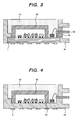
- FIG. 3 illustrates another embodiment of the present invention.
- This embodiment differs from the one shown in FIG. 1 in point of using a metal case 41 instead of the plastic case 40 shown in Fig 1, and using an insulation 45 such as glass to insulate a metal terminal 30 from a metal case 41.
- the use of this configuration reduces the thermal linear expansion coefficient difference between the multilayer substrate 1 and metal case 41. Consequently, no crack may arise between the multilayer substrate 1 and the metal case 41 due to thermal stress of temperature cycle etc., and increases the moisture resistance.
- FIG. 4 illustrates another embodiment, which differs from the embodiments shown in FIGs. 1 to 3 in that the multilayer substrate 1 and the case (40 or 41) are combined into a single unit 42 instead of being separated from each other.
- the above combined single unit 42 be made of an organic material due to cost considerations. However, it may also be made of an inorganic-material.
- FIG. 5 illustrates another embodiment, which differs from the embodiment shown in FIG. 4 in that a separate structure is employed for the antenna pattern 2. That is, a substrate which the antenna pattern 2a is formed separates from the case 42. This configuration increases the flexibility of the design for antenna characteristic.
- FIG. 6 illustrates another embodiment in which an inorganic multilayer substrate 3 is manufactured by using a multilayer substrate 1A and its member 1B.
- the member 1B is constituted with same material as multilayer substrate 3.
- the member 1B constitutes a wall for making a hollow structure around the MMICs 10, 11.
- a metal cover 51 is joined to the member 1B with brazing filler metal 65 such as solder etc. to seal the hollow structure keeping airtight. That is, the member 1B and the metal cover 51 are used instead of the cap 50 shown in Fig 1 to Figs.
- FIG. 7 illustrates one embodiment of a multilayer substrate 1.
- An MMIC chip 15, a microcomputer chip 16, a clock oscillator 17, and a filter capacitor 18 are mounted on the multilayer substrate 1. Further, signal separation is provided, for instance, for an analog signal ground 6 and a digital signal ground 5. The opposite surface of the multilayer substrate 1 is provided with an antenna pattern 2.
- the above configuration makes it possible to turn the whole millimeter wave radar into a module.
- the present invention which has been described above, provides good electrical characteristics of millimeter waves since it has a hollow structure around MMICs on a multilayer substrate. Furthermore, since the whole within a case in which houses electric parts is covered a gelled organic resin which has moisture resistance, it is possible to provide a low-cost millimeter wave radar RF module having increased productivity while maintaining the millimeter wave electrical characteristics even though airtightness is not assured.
Landscapes
- Engineering & Computer Science (AREA)
- Radar, Positioning & Navigation (AREA)
- Remote Sensing (AREA)
- Computer Networks & Wireless Communication (AREA)
- Physics & Mathematics (AREA)
- General Physics & Mathematics (AREA)
- Radar Systems Or Details Thereof (AREA)
- Variable-Direction Aerials And Aerial Arrays (AREA)
- Details Of Aerials (AREA)
Abstract
An object of the present invention is to provide a
millimeter wave radar device and module that provides a
hollow structure while assuring adequate moisture
resistance.
A multilayer substrate (1) on which at least one
millimeter wave MMIC (10) is mounted and a cap (50) for
forming a hollow around the MMIC (10) are joined together
with an adhesive (60) or other similar organic member to
obtain a high-frequency characteristic. The resulting
assembly is housed in a case (40) and covered with a
moisture resistance by a gelled organic resin (70). The
nonairtight structure obtained in this manner permits the
use of low-cost members and provides increased productivity.
Description
- The present invention relates to a vehicle-mounted millimeter wave radar device, millimeter wave radar module, and manufacturing method thereof.
- Japanese Application Patent Laid-open Publication No. Hei 7-273237A discloses a semiconductor device in which a hollow is provided around an IC chip and sealed up with a structure composed of a first cap, a molded resin, and a second cap. The molded resin is cured by baking after it is covered with the second cap. Since the device has the hollow around the IC chip, it is possible to prevent IC bonding wires from being cut by thermal stress caused by plastic molding. Furthermore, deterioration of the electrical characteristics can be prevented in comparison with a device in which an IC chip is directly covered by resin, by making a hollow structure around the IC chip.
- In a high frequency or other millimeter wave radar RF (Radio Frequency) module, the above conventional technology provides a hollow structure to prevent deterioration in the millimeter wave electrical characteristic. However it fails to assure adequate moisture resistance, and it cannot provide a low-cost millimeter wave radar RF module.
- It is the object of the present invention to provide a millimeter wave radar device and module that provides a hollow structure while assuring adequate moisture resistance.
- The above object is achieved by a vehicle-mounted millimeter wave radar device that comprises a millimeter wave generation means for generating millimeter waves, an antenna means for sending out millimeter waves, a substrate provided with wiring and the millimeter wave generation means, an enclosure joined to the substrate to enclose the millimeter wave generation means and the surrounding space on the substrate in cooperation with the substrate, and a resin covers the joint between the enclosure and the substrate at least.
- A multilayer substrate on which at least one MMIC (Monolithic Microwave Integrated Circuit) for a millimeter wave radar is mounted and a cap for forming a hollow around the MMIC are joined together with an adhesive or other similar organic member to obtain a high-frequency characteristic. The resulting assembly is housed in a case and covered with a moisture resistance by a gelled organic resin. The nonairtight structure obtained in this manner permits the use of low-cost members and provides increased productivity.
- Further, the above object is achieved by a method for manufacturing a millimeter wave radar module that sends out radar waves generated by at least one MMIC via an antenna pattern. This method comprises the steps of mounting the MMIC on a wired substrate, enclosing the MMIC by joining a cap containing a hollow to the substrate in such a manner as to position the MMIC in the hollow, and covering the joint with a gel.
-
- FIG. 1 is a cross-sectional view illustrating the structure of one embodiment of the present invention.
- FIG. 2 illustrates another embodiment of the present invention.
- FIG. 3 illustrates another embodiment of the present invention.
- FIG. 4 illustrates another embodiment of the present invention.
- FIG. 5 illustrates another embodiment of the present invention.
- FIG. 6 illustrates another embodiment of the present invention.
- FIG. 7 illustrates one embodiment of a multilayer substrate that is used in a configuration for the present invention.
-
- One embodiment of the present invention will now be described with reference to FIG. 1.
- A circuit substrate is formed by soldering or wire-bonding
MMICs pads 13 to amultilayer substrate 1, which is formed together with anantenna pattern 2 as one piece. For example, the antenna is comprised of a patch antenna. - A
cap 50 is joined to the above circuit substrate with anorganic adhesive 60 to make a hollow structure around a circuit section comprised of the MMICs (a millimeter wave generation means) 10, 11. - The hollow structure may be made by performing a juncture process for the
cap 50 within nitrogen gas, and be filled with sealinggas 100 as for example nitrogen gas etc. - Further, the hollow structure may contain a moisture absorbent (not shown) to protect the MMICs from moisture.
- A
plastic case 40 into which ametal terminal 30 is inserted is joined to a fringe of the multilayer substrate with anorganic adhesive 60. In the inside of theplastic case 40, awire 20 is connected between thepad 13 and themetal terminal 30, and agel 70 of silicone or the like is filled as a filler except the inside of thecap 50. - The present embodiment, which is configured as described above, has the hollow structure for the MMIC section to provide simple hermetical sealing, retains millimeter waves or other high-frequency electrical characteristics and effectively uses a gel to provide protection against moisture.
- FIG. 2 illustrates another embodiment of the present invention. This embodiment differs from the embodiment shown in FIG. 1 in point of joining a
plastic cover 80 to theplastic case 40 with anorganic adhesive 60. Theplastic cover 80 covers an upper opening of theplastic case 40. The present embodiment provides higher moisture resistance than the embodiment shown in FIG. 1. - FIG. 3 illustrates another embodiment of the present invention. This embodiment differs from the one shown in FIG. 1 in point of using a
metal case 41 instead of theplastic case 40 shown in Fig 1, and using aninsulation 45 such as glass to insulate ametal terminal 30 from ametal case 41. The use of this configuration reduces the thermal linear expansion coefficient difference between themultilayer substrate 1 andmetal case 41. Consequently, no crack may arise between themultilayer substrate 1 and themetal case 41 due to thermal stress of temperature cycle etc., and increases the moisture resistance. - FIG. 4 illustrates another embodiment, which differs from the embodiments shown in FIGs. 1 to 3 in that the
multilayer substrate 1 and the case (40 or 41) are combined into asingle unit 42 instead of being separated from each other. - The use of the above configuration reduces the cost.
- It is preferable that the above combined
single unit 42 be made of an organic material due to cost considerations. However, it may also be made of an inorganic-material. - FIG. 5 illustrates another embodiment, which differs from the embodiment shown in FIG. 4 in that a separate structure is employed for the
antenna pattern 2. That is, a substrate which the antenna pattern 2a is formed separates from thecase 42. This configuration increases the flexibility of the design for antenna characteristic. - FIG. 6 illustrates another embodiment in which an
inorganic multilayer substrate 3 is manufactured by using amultilayer substrate 1A and itsmember 1B. Themember 1B is constituted with same material asmultilayer substrate 3. - The
member 1B constitutes a wall for making a hollow structure around theMMICs metal cover 51 is joined to themember 1B withbrazing filler metal 65 such as solder etc. to seal the hollow structure keeping airtight. That is, themember 1B and themetal cover 51 are used instead of thecap 50 shown in Fig 1 to Figs. - FIG. 7 illustrates one embodiment of a
multilayer substrate 1. An MMICchip 15, amicrocomputer chip 16, aclock oscillator 17, and afilter capacitor 18 are mounted on themultilayer substrate 1. Further, signal separation is provided, for instance, for ananalog signal ground 6 and adigital signal ground 5. The opposite surface of themultilayer substrate 1 is provided with anantenna pattern 2. - The above configuration makes it possible to turn the whole millimeter wave radar into a module.
- The present invention, which has been described above, provides good electrical characteristics of millimeter waves since it has a hollow structure around MMICs on a multilayer substrate. Furthermore, since the whole within a case in which houses electric parts is covered a gelled organic resin which has moisture resistance, it is possible to provide a low-cost millimeter wave radar RF module having increased productivity while maintaining the millimeter wave electrical characteristics even though airtightness is not assured.
Claims (18)
- A vehicle-mounted millimeter wave radar device that detects objects by sending out millimeter waves, comprising:a millimeter wave generation means (10,11) for generating millimeter waves;an antenna means (2) for sending out said millimeter waves;a substrate (1) that is provided with wiring and said millimeter wave generation means (10,11);an enclosure (50) that is joined to said substrate (1) to enclose said millimeter wave generation means (10,11) and the surrounding space on said substrate (1) in cooperation with said substrate (1); anda resin (70) that covers the joint (60) between said enclosure (50) and said substrate (1) at least.
- The vehicle-mounted millimeter wave radar device according to claim 1, comprising means (80) for preventing outflow of said resin (70), wherein said antenna means (2) is provided on a surface of said substrate (1) opposite to the surface mounting said millimeter wave generation means (10,11).
- The vehicle-mounted millimeter wave radar device according to claim 1, wherein said space is filled with an inert gas.
- The vehicle-mounted millimeter wave radar device according to claim 1, wherein said enclosure (50) includes means for moisture absorption.
- A millimeter wave radar module equipped with at least one MMIC (10) for millimeter waves which is mounted on a multilayer substrate (1),
wherein a patch antenna circuit (2) is formed on a surface of said multilayer substrate (1); said MMIC (10) are provided on the remaining surface; said multilayer substrate (1) is housed in a case (40) which input/output signal terminals (30) is put through; a hollow cap (50) for protecting said MMIC (10) is joined to the surface on which said MMIC (10) is provided, and said cap (50) is covered with a moisture resistance resin (70). - The millimeter wave radar module according to claim 5, wherein a cover (80) covers said moisture resistance resin (70).
- The millimeter wave radar module according to claim 5, wherein said case (40) is made of a conductive material; the circumference of said input/output signal terminals (30) is made of an insulation material, and said input/output signal terminals (30) are put through said case (40) with said insulation material (45).
- The millimeter wave radar module according to claim 5, wherein said multilayer substrate (1) is integral with said case (40).
- The millimeter wave radar module according to claim 5, wherein said MMIC (10) is provided on said multilayer substrate (1), and said patch antenna circuit (2) is formed by a separate member.
- The millimeter wave radar module according to claim 5, wherein said multilayer substrate (1) is not planar structure but shaped so as to contain a space, and wherein a flat cover (51) is joined to said multilayer substrate (1) so as to provide a hollow storage space for said MMIC (10).
- The millimeter wave radar module according to claim 5, wherein said storage space for said MMIC (10) houses a moisture absorbent.
- The millimeter wave radar module according to claim 5, wherein said storage space for said MMIC (10) is filled with an inert gas.
- The millimeter wave radar module according to claim 5, wherein said multilayer substrate (1) is made of either an inorganic material or an organic material.
- The millimeter wave radar module according to claim 5, wherein said hollow cap (50) and said multilayer substrate (1) are joined by an organic material using as an adhesive.
- The millimeter wave radar module according to claim 5, wherein said moisture resistance resin (70) is a gelled organic resin.
- A method for manufacturing a millimeter wave radar module that sends out radar waves generated by at least one MMIC (10) via an antenna pattern (2), the method comprising the steps of:mounting said MMIC (10) on a substrate (1) with wiring;enclosing said MMIC (10) by joining a cap (50) containing a hollow to said substrate (1) in such a manner as to position said MMIC (10) in said hollow; andcovering said the joint between said cap (50) and said substrate (1) at least with a gel (70).
- The method according to claim 16, wherein said juncture is performed in a nitrogen gas atmosphere.
- The method according to claim 16, wherein said substrate (1) is provided with a wall (1B) that forms an enclosure, and wherein said gel is filled into said enclosure after said juncture.
Applications Claiming Priority (2)
| Application Number | Priority Date | Filing Date | Title |
|---|---|---|---|
| JP2002296872 | 2002-10-10 | ||
| JP2002296872A JP3858801B2 (en) | 2002-10-10 | 2002-10-10 | In-vehicle millimeter-wave radar device, millimeter-wave radar module, and manufacturing method thereof |
Publications (1)
| Publication Number | Publication Date |
|---|---|
| EP1422534A1 true EP1422534A1 (en) | 2004-05-26 |
Family
ID=32089248
Family Applications (1)
| Application Number | Title | Priority Date | Filing Date |
|---|---|---|---|
| EP03022982A Withdrawn EP1422534A1 (en) | 2002-10-10 | 2003-10-10 | Vehicle-mounted millimeter wave radar device, millimeter wave radar module, and manufacturing method thereof |
Country Status (3)
| Country | Link |
|---|---|
| US (2) | US7098842B2 (en) |
| EP (1) | EP1422534A1 (en) |
| JP (1) | JP3858801B2 (en) |
Families Citing this family (25)
| Publication number | Priority date | Publication date | Assignee | Title |
|---|---|---|---|---|
| DE102004029440A1 (en) * | 2004-06-18 | 2006-01-12 | Infineon Technologies Ag | Transmitting / receiving device |
| JP4189970B2 (en) * | 2004-11-05 | 2008-12-03 | 株式会社日立製作所 | Antenna device |
| US8106307B2 (en) * | 2006-01-26 | 2012-01-31 | Panasonic Corporation | Substrate structure and electronic apparatus |
| IL173941A0 (en) * | 2006-02-26 | 2007-03-08 | Haim Goldberger | Monolithic modules for high frequecney applications |
| JP4286855B2 (en) * | 2006-09-07 | 2009-07-01 | 株式会社日立製作所 | Radar equipment |
| US7492313B1 (en) * | 2006-10-31 | 2009-02-17 | Lockheed Martin Corporation | Digital processing radar system |
| US7675465B2 (en) * | 2007-05-22 | 2010-03-09 | Sibeam, Inc. | Surface mountable integrated circuit packaging scheme |
| US8345716B1 (en) | 2007-06-26 | 2013-01-01 | Lockheed Martin Corporation | Polarization diverse antenna array arrangement |
| US7705761B2 (en) * | 2007-11-07 | 2010-04-27 | Lockheed Martin Corporation | System and method for wideband direct sampling and beamforming using complex analog to digital converter |
| US7733265B2 (en) * | 2008-04-04 | 2010-06-08 | Toyota Motor Engineering & Manufacturing North America, Inc. | Three dimensional integrated automotive radars and methods of manufacturing the same |
| US8022861B2 (en) | 2008-04-04 | 2011-09-20 | Toyota Motor Engineering & Manufacturing North America, Inc. | Dual-band antenna array and RF front-end for mm-wave imager and radar |
| US7830301B2 (en) * | 2008-04-04 | 2010-11-09 | Toyota Motor Engineering & Manufacturing North America, Inc. | Dual-band antenna array and RF front-end for automotive radars |
| KR101581225B1 (en) * | 2008-11-07 | 2015-12-30 | 시빔, 인코퍼레이티드 | Surface mountable integrated circuit packaging means |
| US7990237B2 (en) * | 2009-01-16 | 2011-08-02 | Toyota Motor Engineering & Manufacturing North America, Inc. | System and method for improving performance of coplanar waveguide bends at mm-wave frequencies |
| US8786496B2 (en) | 2010-07-28 | 2014-07-22 | Toyota Motor Engineering & Manufacturing North America, Inc. | Three-dimensional array antenna on a substrate with enhanced backlobe suppression for mm-wave automotive applications |
| US8279100B2 (en) | 2010-09-30 | 2012-10-02 | Lockheed Martin Corporation | Complex analog to digital converter (CADC) system on chip double rate architecture |
| US8854255B1 (en) | 2011-03-28 | 2014-10-07 | Lockheed Martin Corporation | Ground moving target indicating radar |
| CN104718804B (en) * | 2012-10-03 | 2018-10-23 | 新电元工业株式会社 | Electronic equipment |
| DE102014109120B4 (en) | 2014-06-30 | 2017-04-06 | Krohne Messtechnik Gmbh | microwave module |
| US10411329B2 (en) | 2016-01-20 | 2019-09-10 | Apple Inc. | Packaged devices with antennas |
| KR20180054079A (en) * | 2016-11-15 | 2018-05-24 | 인지니어스 주식회사 | Radar module including screen board |
| US10910706B2 (en) * | 2018-01-19 | 2021-02-02 | Mediatek Inc. | Radar sensor housing design |
| US12113300B2 (en) * | 2018-05-10 | 2024-10-08 | Richwave Technology Corp. | Doppler motion sensor device with high isolation between antennas |
| JP7211333B2 (en) * | 2019-10-30 | 2023-01-24 | 株式会社デンソー | Electronics |
| DE102024112205A1 (en) * | 2024-04-30 | 2025-10-30 | Vega Grieshaber Kg | High-frequency chip arrangement, sensor and manufacturing process |
Citations (5)
| Publication number | Priority date | Publication date | Assignee | Title |
|---|---|---|---|---|
| JPH07273237A (en) * | 1994-03-30 | 1995-10-20 | Nec Corp | Semiconductor device and its manufacture |
| US5955752A (en) * | 1997-06-13 | 1999-09-21 | Fujitsu Limited | Semiconductor module having antenna element therein |
| EP0978729A2 (en) * | 1998-08-07 | 2000-02-09 | Hitachi, Ltd. | High-frequency transmitter-receiving apparatus for such an application as vehicle-onboard radar system |
| WO2000045462A1 (en) * | 1999-01-28 | 2000-08-03 | Robert Bosch Gmbh | Housing for an electronic apparatus in microwave technology |
| WO2003040754A1 (en) * | 2001-11-09 | 2003-05-15 | Hitachi, Ltd. | Mobile millimetric wave radar |
Family Cites Families (5)
| Publication number | Priority date | Publication date | Assignee | Title |
|---|---|---|---|---|
| JP3308734B2 (en) * | 1994-10-13 | 2002-07-29 | 本田技研工業株式会社 | Radar module |
| DE69729344T8 (en) * | 1996-04-03 | 2005-02-17 | Honda Giken Kogyo K.K. | Radar module and MMIC arrangement for it |
| US5943558A (en) * | 1996-09-23 | 1999-08-24 | Communications Technology, Inc. | Method of making an assembly package having an air tight cavity and a product made by the method |
| JP2000114413A (en) * | 1998-09-29 | 2000-04-21 | Sony Corp | Semiconductor device, manufacturing method thereof, and component mounting method |
| JP2004031651A (en) * | 2002-06-26 | 2004-01-29 | Sony Corp | Element mounting board and method of manufacturing the same |
-
2002
- 2002-10-10 JP JP2002296872A patent/JP3858801B2/en not_active Expired - Fee Related
-
2003
- 2003-10-09 US US10/681,246 patent/US7098842B2/en not_active Expired - Fee Related
- 2003-10-10 EP EP03022982A patent/EP1422534A1/en not_active Withdrawn
-
2006
- 2006-07-07 US US11/482,056 patent/US7355547B2/en not_active Expired - Fee Related
Patent Citations (5)
| Publication number | Priority date | Publication date | Assignee | Title |
|---|---|---|---|---|
| JPH07273237A (en) * | 1994-03-30 | 1995-10-20 | Nec Corp | Semiconductor device and its manufacture |
| US5955752A (en) * | 1997-06-13 | 1999-09-21 | Fujitsu Limited | Semiconductor module having antenna element therein |
| EP0978729A2 (en) * | 1998-08-07 | 2000-02-09 | Hitachi, Ltd. | High-frequency transmitter-receiving apparatus for such an application as vehicle-onboard radar system |
| WO2000045462A1 (en) * | 1999-01-28 | 2000-08-03 | Robert Bosch Gmbh | Housing for an electronic apparatus in microwave technology |
| WO2003040754A1 (en) * | 2001-11-09 | 2003-05-15 | Hitachi, Ltd. | Mobile millimetric wave radar |
Non-Patent Citations (1)
| Title |
|---|
| PATENT ABSTRACTS OF JAPAN vol. 1996, no. 02 29 February 1996 (1996-02-29) * |
Also Published As
| Publication number | Publication date |
|---|---|
| US7098842B2 (en) | 2006-08-29 |
| US20040075604A1 (en) | 2004-04-22 |
| US20060250298A1 (en) | 2006-11-09 |
| US7355547B2 (en) | 2008-04-08 |
| JP2004134541A (en) | 2004-04-30 |
| JP3858801B2 (en) | 2006-12-20 |
Similar Documents
| Publication | Publication Date | Title |
|---|---|---|
| US7355547B2 (en) | Vehicle-mounted millimeter wave radar device, millimeter wave radar module, and manufacturing method thereof | |
| US5498903A (en) | Surface mountable integrated circuit package with integrated battery mount | |
| US5468910A (en) | Semiconductor device package and method of making | |
| US5293301A (en) | Semiconductor device and lead frame used therein | |
| US6518501B1 (en) | Electronic part and method of assembling the same | |
| US6215175B1 (en) | Semiconductor package having metal foil die mounting plate | |
| JP2811170B2 (en) | Resin-sealed semiconductor device and method of manufacturing the same | |
| US5656857A (en) | Semiconductor device with insulating resin layer and substrate having low sheet resistance | |
| JPH02342A (en) | Attachment of integrated circuit chip and package assembly | |
| EP3648158A1 (en) | Shielded semiconductor device and lead frame therefor | |
| US5932927A (en) | High-frequency device package | |
| CN111201597A (en) | Rivetless Lead Fastening for Semiconductor Packages | |
| JPH0685126A (en) | Semiconductor device | |
| JP2621722B2 (en) | Semiconductor device | |
| KR19990032607A (en) | Air-cavity plastic package and its manufacturing method | |
| JPH06112348A (en) | Hybrid circuit | |
| KR19990034054A (en) | Air-cavity plastic package with heat sink and manufacturing method | |
| JP3440136B2 (en) | Collective electronic components | |
| JPH07321243A (en) | Semiconductor device and manufacturing method thereof | |
| JP2549633Y2 (en) | Power module | |
| JPH1145960A (en) | Semiconductor device and manufacturing method thereof | |
| JPH01215049A (en) | Semiconductor device | |
| JPS5942456B2 (en) | Hybrid integrated circuit device | |
| JPH03273667A (en) | Resin seal type hybrid integrated circuit | |
| JPH0864760A (en) | Semiconductor device |
Legal Events
| Date | Code | Title | Description |
|---|---|---|---|
| PUAI | Public reference made under article 153(3) epc to a published international application that has entered the european phase |
Free format text: ORIGINAL CODE: 0009012 |
|
| AK | Designated contracting states |
Kind code of ref document: A1 Designated state(s): AT BE BG CH CY CZ DE DK EE ES FI FR GB GR HU IE IT LI LU MC NL PT RO SE SI SK TR |
|
| AX | Request for extension of the european patent |
Extension state: AL LT LV MK |
|
| 17P | Request for examination filed |
Effective date: 20040917 |
|
| AKX | Designation fees paid |
Designated state(s): DE FR GB IT |
|
| 17Q | First examination report despatched |
Effective date: 20060905 |
|
| STAA | Information on the status of an ep patent application or granted ep patent |
Free format text: STATUS: THE APPLICATION HAS BEEN WITHDRAWN |
|
| 18W | Application withdrawn |
Effective date: 20090310 |