EP1418745A2 - Scan line non-linearity compensation system in a raster output scanner - Google Patents
Scan line non-linearity compensation system in a raster output scanner Download PDFInfo
- Publication number
- EP1418745A2 EP1418745A2 EP03025473A EP03025473A EP1418745A2 EP 1418745 A2 EP1418745 A2 EP 1418745A2 EP 03025473 A EP03025473 A EP 03025473A EP 03025473 A EP03025473 A EP 03025473A EP 1418745 A2 EP1418745 A2 EP 1418745A2
- Authority
- EP
- European Patent Office
- Prior art keywords
- linearity
- pixel
- system architecture
- scan
- correction
- Prior art date
- Legal status (The legal status is an assumption and is not a legal conclusion. Google has not performed a legal analysis and makes no representation as to the accuracy of the status listed.)
- Withdrawn
Links
Images
Classifications
-
- G—PHYSICS
- G06—COMPUTING; CALCULATING OR COUNTING
- G06K—GRAPHICAL DATA READING; PRESENTATION OF DATA; RECORD CARRIERS; HANDLING RECORD CARRIERS
- G06K15/00—Arrangements for producing a permanent visual presentation of the output data, e.g. computer output printers
- G06K15/02—Arrangements for producing a permanent visual presentation of the output data, e.g. computer output printers using printers
- G06K15/12—Arrangements for producing a permanent visual presentation of the output data, e.g. computer output printers using printers by photographic printing, e.g. by laser printers
- G06K15/1204—Arrangements for producing a permanent visual presentation of the output data, e.g. computer output printers using printers by photographic printing, e.g. by laser printers involving the fast moving of an optical beam in the main scanning direction
- G06K15/1219—Detection, control or error compensation of scanning velocity or position, e.g. synchronisation
-
- H—ELECTRICITY
- H04—ELECTRIC COMMUNICATION TECHNIQUE
- H04N—PICTORIAL COMMUNICATION, e.g. TELEVISION
- H04N1/00—Scanning, transmission or reproduction of documents or the like, e.g. facsimile transmission; Details thereof
- H04N1/04—Scanning arrangements, i.e. arrangements for the displacement of active reading or reproducing elements relative to the original or reproducing medium, or vice versa
- H04N1/047—Detection, control or error compensation of scanning velocity or position
- H04N1/053—Detection, control or error compensation of scanning velocity or position in main scanning direction, e.g. synchronisation of line start or picture elements in a line
-
- H—ELECTRICITY
- H04—ELECTRIC COMMUNICATION TECHNIQUE
- H04N—PICTORIAL COMMUNICATION, e.g. TELEVISION
- H04N1/00—Scanning, transmission or reproduction of documents or the like, e.g. facsimile transmission; Details thereof
- H04N1/04—Scanning arrangements, i.e. arrangements for the displacement of active reading or reproducing elements relative to the original or reproducing medium, or vice versa
- H04N1/113—Scanning arrangements, i.e. arrangements for the displacement of active reading or reproducing elements relative to the original or reproducing medium, or vice versa using oscillating or rotating mirrors
- H04N1/1135—Scanning arrangements, i.e. arrangements for the displacement of active reading or reproducing elements relative to the original or reproducing medium, or vice versa using oscillating or rotating mirrors for the main-scan only
-
- H—ELECTRICITY
- H04—ELECTRIC COMMUNICATION TECHNIQUE
- H04N—PICTORIAL COMMUNICATION, e.g. TELEVISION
- H04N2201/00—Indexing scheme relating to scanning, transmission or reproduction of documents or the like, and to details thereof
- H04N2201/04—Scanning arrangements
- H04N2201/047—Detection, control or error compensation of scanning velocity or position
- H04N2201/04701—Detection of scanning velocity or position
- H04N2201/0471—Detection of scanning velocity or position using dedicated detectors
- H04N2201/04712—Detection of scanning velocity or position using dedicated detectors using unbroken arrays of detectors, i.e. detectors mounted on the same substrate
-
- H—ELECTRICITY
- H04—ELECTRIC COMMUNICATION TECHNIQUE
- H04N—PICTORIAL COMMUNICATION, e.g. TELEVISION
- H04N2201/00—Indexing scheme relating to scanning, transmission or reproduction of documents or the like, and to details thereof
- H04N2201/04—Scanning arrangements
- H04N2201/047—Detection, control or error compensation of scanning velocity or position
- H04N2201/04701—Detection of scanning velocity or position
- H04N2201/04734—Detecting at frequent intervals, e.g. once per line for sub-scan control
-
- H—ELECTRICITY
- H04—ELECTRIC COMMUNICATION TECHNIQUE
- H04N—PICTORIAL COMMUNICATION, e.g. TELEVISION
- H04N2201/00—Indexing scheme relating to scanning, transmission or reproduction of documents or the like, and to details thereof
- H04N2201/04—Scanning arrangements
- H04N2201/047—Detection, control or error compensation of scanning velocity or position
- H04N2201/04701—Detection of scanning velocity or position
- H04N2201/04744—Detection of scanning velocity or position by detecting the scanned beam or a reference beam
-
- H—ELECTRICITY
- H04—ELECTRIC COMMUNICATION TECHNIQUE
- H04N—PICTORIAL COMMUNICATION, e.g. TELEVISION
- H04N2201/00—Indexing scheme relating to scanning, transmission or reproduction of documents or the like, and to details thereof
- H04N2201/04—Scanning arrangements
- H04N2201/047—Detection, control or error compensation of scanning velocity or position
- H04N2201/04753—Control or error compensation of scanning position or velocity
- H04N2201/04758—Control or error compensation of scanning position or velocity by controlling the position of the scanned image area
- H04N2201/04767—Control or error compensation of scanning position or velocity by controlling the position of the scanned image area by controlling the timing of the signals, e.g. by controlling the frequency o phase of the pixel clock
- H04N2201/04768—Controlling the frequency of the signals
- H04N2201/04777—Controlling the frequency of the signals using a voltage controlled oscillator
-
- H—ELECTRICITY
- H04—ELECTRIC COMMUNICATION TECHNIQUE
- H04N—PICTORIAL COMMUNICATION, e.g. TELEVISION
- H04N2201/00—Indexing scheme relating to scanning, transmission or reproduction of documents or the like, and to details thereof
- H04N2201/04—Scanning arrangements
- H04N2201/047—Detection, control or error compensation of scanning velocity or position
- H04N2201/04753—Control or error compensation of scanning position or velocity
- H04N2201/04793—Control or error compensation of scanning position or velocity using stored control or compensation data, e.g. previously measured data
Definitions
- the present invention relates to a system architecture for scan line non-linearity in a Raster Output Scanning (ROS) system and, more particularly, to a system architecture that enables correction of scan non-linearity and "mix and match" of ROS units and pixel boards at random during the manufacture of printing systems.
- ROS Raster Output Scanning
- the printer typically uses a Raster Output Scanner (ROS) to expose the charged portions of a photosensitive medium, such as a photoreceptor, to record an electrostatic latent image on the photosensitive medium.
- ROS Raster Output Scanner
- a plurality of ROS units can be used in a color xerographic ROS printer.
- Each ROS forms a scan line for a separate color image on a common photoreceptor belt.
- Each color image is developed in overlying registration with the other color images from the other ROS units to form a composite color image that is transferred to an output sheet.
- Registration of each scan line of the plurality of ROS units requires each image to be registered to within a 0.1 mm circle or within a tolerance of ⁇ 0.05 mm.
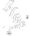
- a typical prior art raster output scanning system 10 of FIG. 1 includes a light source 12 for generating a light beam 14 and scanning means 16 for directing the light beam 14 to a spot 18 at a photosensitive medium 20 .
- the scanning means 16 also serves to move the spot 18 along a scan line 22 of specified length at the photosensitive medium 20 .
- the scanning means 16 in the illustrated scanner system 10 includes a rotatable polygon mirror with a plurality of light reflecting facets 24 (eight facets being illustrated) and other known mechanical components that are depicted in FIG.1 by the polygon 16 rotating about a rotational axis 26 in the direction of an arrow 28.
- the light source, 12 such as a laser diode, emits a modulated coherent light beam 14 of a single wavelength.
- the light beam 14 is modulated in conformance with the image information data stream contained in the video signal sent from image output light source control circuit 30 to the light source 12 .
- the modulated light beam 14 is collimated by a collimating lens 32, then focused by a cross-scan cylindrical lens 34 to form a line on a reflective facet 24 of the rotating polygon mirror 16 .
- the polygon mirror 16 is rotated around its axis of rotation by a conventional motor (not shown), known to those of ordinary skill in the art.
- the beam 14 reflected from the facet 24 then passes through the f-theta scan lenses 36 and the anamorphic wobble correction lens 38 .
- the f-theta scan lens 36 consists of a negative piano-spherical lens 40, a positive piano-spherical lens 42, and the cross-scan cylinder lens 44.
- This configuration of f-theta scan lenses has sufficient negative distortion to produce a linear scan beam.
- the light beam will be deflected at a constant angular velocity from the rotating mirror that the f-theta scan lens optically modifies to scan the surface at a nearly constant linear velocity.
- the f-theta scan lens 36 will focus the light beam 14 in the scan plane onto the scan line 22 on the photosensitive medium 20.
- the wobble correction optical element 38 can be a lens or a mirror and is sometimes referred to as the "motion compensating optics".
- the purpose of optical element 38 is to correct wobble along the scan line generated by inaccuracies in the polygon mirror / motor assembly.
- the wobble correction lens 38 focuses the light beam in the cross-scan plane onto the scan line 22 on the photosensitive medium 20.
- the light beam 14 is reflected by the facets 24 through the f-theta and wobble correction lenses and scans across the surface of the photosensitive medium in a known manner along the scan line 22 from a first end 46 of the scan line 22 (Start of Scan or "SOS") past a center (the illustrated position of the spot 18) and on to a second end 48 of the scan line 22 (End of Scan or "EOS").
- the light beam exposes an electrostatic latent image on the photosensitive member 20 .
- the exposing light beam 14 is modulated by circuit 30 to produce individual bursts of light that expose a line of individual pixels, or spots 18, on the photosensitive medium 20.
- the ROS should be capable of exposing a line of evenly spaced, identical pixels on the photosensitive medium 20.
- the ROS should be capable of exposing a line of evenly spaced, identical pixels on the photosensitive medium 20.
- manufacturing errors can cause imperfections in the scan optics, obtaining evenly spaced, identical pixels can be problematic.
- Scan non-linearity refers to variations in pixel placement relative to uniform pixel placement, and this is primarily due to variation of the spot velocity occurring as the spot moves along the scan line during the scan cycle relative.
- Scan linearity is the measure of how equally spaced the spots are written in the scan direction across the entire scanline.
- reference points on the scan line must first be specified: one definition is to consider that the two idealized ends of the scan line have zero error, provided that the delay from SOS to the first active is adjusted correctly (correct margin adjustment) and provided the last pixel of the active scanline is also adjusted correctly (correct magnification adjustment).
- Active scan is defined as that part of the scan line, which is modulated by the video stream.
- typical scan linearity curves start at zero position error at one end of the active scan and end with zero position error at the other end of active scan.
- the non-linearity curve can have a multitude of shapes. Ideally, the curve of non-linearity versus scan distance would be at zero across the entire scanline for perfect pixel placement. From optical modeling for one lens design, the ideal shape would appear as in FIG. 4. In practice the shape may have only one lobe (above or below) the zero non-linearity line, or non-symmetrical lobes that are distorted from the sinusoidal-like appearance and the number of zero crossings of non-linearity of the ROS can vary from unit to unit.
- Scan non-linearity is typically caused by system geometry or a velocity variation of the scanning means.
- the speed at which the focussed exposing light beam travels across the scan line on the photosensitive medium 20 is called the spot velocity.
- the spot velocity will vary as the light beam scans across the photosensitive medium.
- the video input of some raster output scanners compensate for such non-linearity electronically using a variable frequency pixel clock (sometimes called a scanning clock).
- the pixel clock produces a pulse train (i.e., a pixel clock signal) that is used to turn the light beam emitted by the light source on and off at each pixel position along the scan line.
- a pulse train i.e., a pixel clock signal
- the resulting pixels will be advanced or retarded relative to the uniform pixel placement because of scan non-linearity of the ROS.
- the pixels can be place with minimal deviation from the ideal of equally space pixels. That will more evenly space the pixels and thereby at least partially compensate for what is sometimes called pixel position distortion (i.e., uneven pixel spacing caused by scanner non-linearity).
- the pixel clock control circuitry 30 serves as an electronic control system for synchronizing the light beam 14 modulation in order to produce the pixels along the scan line 22.
- the control system that includes video and pixel clock may, for example, be configured using known components and design techniques to produce a control signal for activating the light beam at each of a plurality of desired pixel positions along the scan line (e.g., the central portion of each pixel position being evenly spaced at 1/300 inch intervals for 300 dpi resolution or being evenly spaced at 1/600 inch intervals for 600 dpi resolution, etcetera).
- control system is configured so that the control signal defines a pixel interval for each pixel position and so that the pixel interval defined by the control signal varies according to spot velocity, to correct for scan non-linearity as described above.
- the control system may also synchronize the control signal with spot position by suitable known means, such as by responding to a start-of-scan (SOS) control signal or other synchronizing signal produced by known means, in order to enable alignment of the start of the sequence of pixels in each scanline.
- SOS start-of-scan
- This sequence of pixels is delayed by a defined clock count in order to set the edge margin of the active scan scanline.
- the average clock frequency can also be adjusted to change the scan magnification.
- the scan magnification is decreased and conversely if the average clock frequency is decreased the scan magnification is increased.
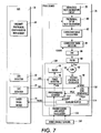
- the settings of margin and magnification are sensed by marks on the photoreceptor as shown by block 118 in FIG. 7.
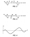
- FIG. 2 shows a an ideal scan line 100 consisting of a series of pixels 102 uniformly spaced 104 by the pixel clock of the raster output scanning system. These pixels 102 on the scan line 100 are placed on a uniform grid 106 at each clock cycle in the idealized case of perfect scan non-linearity.
- FIG. 3 illustrates deviation from the uniform pixel placement of FIG. 2 due to scan non-linearity.
- the scan line 200 consists of a series of pixels 202 which are displaced by a distance 204 from the uniform pixel placement 206 along the scan line as shown schematically in the graph of FIG. 4.
- Pixel clock frequency variation is used to compensate for this profile.
- a lookup table is used to control the pixel clock frequency variation, according to a prescribed algorithm.
- the transfer function of clock frequency change vs. table value also varies among pixel boards.
- the present invention is a non-linearity correction-system architecture that enables the "mix and match" of a ROS and a pixel board taken at random during the printing system manufacture.
- a system architecture for scanned non-linearity correction in a printer uses any raster output scanner having scanned non-linearity profile previously stored in memory from a test station installed with any pixel board.
- the pixel board includes a correction table register wherein the pixel board utilizes the scanned non-linearity profile of the raster output scanner to calculate the values in a correction table register to correct for pixel misregistration.
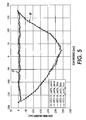
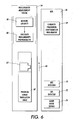
- a ROS Test Station consists of a ROS linearity measurement system 54 for measuring the characteristics of a ROS 56 having exhibiting non-linear characteristics versus scan distance 50 as shown in FIG. 5.
- the ROS linearity measurement system 54 utilizes a CCD camera 62 mounted on a precision linear positioning stage 68.
- a video signal is generated such that 1-on out of every 128 pixels creates an array of spots across the output scan line 66.
- the ROS 56 and the measuring system 54 is configured so that there is only spot seen by the camera 62 at a time.
- the relative position of the spot seen by the camera 62 is determined by measuring the camera position Xcam and the spot centroid Xbar in the camera 62 .
- vscan (Xn -X0) / (Tn -T0)
- a polynomial is then fit to the data (Xi, Yi) and the derivative coefficients are calculated by a computer 60 within the test measurement system 54 .
- the polynomial derivative coefficients 60 are calculated from the polynomial coefficients and these derivative coefficients are then transferred over a communication line (not shown) from the test measurement system to non-volatile memory (NVM) 64 on the ROS control PWBA.
- NVM non-volatile memory
- the non-linearity profile information that is unique to the ROS 56 is saved within the ROS 56 having an end of scan (EOS) detector 70 , start of scan (SOS) detector 72 and laser diode driver 74 for subsequent installation to a printer (not shown).
- a pixel circuit board 76 is connected to the ROS 56 having the linearity derivative polynomial coefficients in NVM 64 during installation.
- the pixel circuit board 76 includes a variable frequency clock with a frequency self-calibration circuit 78 and an imbedded computer.
- the non-linearity of the ROS 56 and the calibration 78 of the clock frequency are each unique.
- the pixel board 76 self-calibrates the clock frequency and then imports the non-linearity coefficients 80 from the ROS 56 over a communication line.
- a lookup table 84 is calculated 82 to adjust the clock frequency as the ROS spot is scanned in a line across the photoreceptor. By speeding up the clock the pixels positions are retarded relative to the beam scanning direction; conversely, by decreasing the clock frequency the pixel placement is advanced relative to the scanning direction.
- FIG. 5 an example of the linearity correction 52 demonstrated with the ROS 56 and pixel board 76 is shown. Therefore, the non-linearity correction algorithm first implemented on the ROS 56 measurement computer is then ported to the computer on the pixel board 76 wherein the correction is performed using any ROS 56 with any pixel board 76.
- a voltage controlled oscillator (VCO) 98 and a phase locked loop 120 are utilized to generate an accurate main clock Mclk for synchronizing the stream of video data that is sent to the laser diode driver 74.
- a phase detector 96 receives an end of scan (EOS) signal from the EOS detector 70 and an end of count (EOC) signal from the programmable counter 112. Based on the phase difference of the received signals, the phase detector 96 generates a pulse which is converted to a voltage by a charge pump (not shown) and sent out as a voltage V d to the voltage controlled oscillator (VCO) 98 through a low pass filter 94 and sum circuit 92.
- EOS end of scan
- EOC end of count
- the low pass filter 94 reduces the noise level of the V d voltage before delivering it to the sum circuit 92.
- the sum circuit 92 sums the V d voltage with the voltage vcor that is derived from the value in the correction table register which are converted to the appropriate voltage by DAC 86 and passed through filter 90.
- the value in the correction table register is chosen based on the corresponding register address value "count" from the programmable counter 112. Count is incremented some integer multiple number of pixels.
- the voltage level of the V d controls the frequency of VCO 98.
- VCO 98 (clock generator) generates a main clock Mclk from the line sync generator 110 for delivery to the scanline buffer 114.
- the line sync generator is synchronized, based upon the input from the SOS detector 72 .
- the Mclk is sent to a divider to divide the Mclk by M to generate an end of count (EOC).
- M is the total number of pixels per scan line. By way of example only, for a 14.4 inch paper with 600 pixels per inch, M is 8640.
- the EOC which indicates the end of the scan line, is sent to the phase detector 96.
- the phase detector 96 compares the EOC to the EOS.
- EOS is a signal being generated within the ROS 56.
- the respective sensor As the scanning laser light beam passes over a dedicated spot on the scan line immediately prior to pixel placement, the respective sensor generates a start of scan SOS.
- the respective sensor As the scanning laser light beam passes over a dedicated spot on the scan line immediately after the end of pixel placement, the respective sensor generates an end of scan EOS.
- the SOS 72 and the EOS 70 are being generated for each scan line. Since the speed of the scanning laser light beam is fixed, the time between the SOS and the EOS is the same for each scan line.
- the EOC has to match the EOS. If they do not match, it means the frequency of the main clock Mclk needs to be decreased or increased depending on if the EOC was prior to or after the EOS respectively. Therefore, depending on if EOC is before or after EOS, the phase detector 96 generates either a positive pulse or a negative pulse respectively. The width of the pulse indicates the time difference between the EOS and EOC. Typically, the timing of EOS and EOC do not match. As a result, the phase detector 96 typically generates either a negative or a positive pulse. However, if the timing of EOS and EOC match, the phase detector 96 does not generate a pulse.
- a charge pump (not shown), and integrator (also not shown) generate a base voltage and send it as voltage V d to the VCO 98.
- the charge pump subtracts or adds a voltage, proportional to the width of the pulse, from/to the integrator's base voltage and sends the result as voltage V d to the VCO 98.
- V d is equal to the base voltage since there is no EOC to be compared to the EOS. Therefore, the first V d causes the VCO 98 to calibrate the frequency of the Mclk to a reference frequency (54 MHz by way of example). Subsequently, at the end of each scan line, depending on if EOC deviates from or matches the EOS, a new or the same V d will be sent out by the integrator, respectively.
- the frequency of the Mclk does not change. However, if a new V d is sent out, the deviation of V d from the base voltage causes the VCO to re-calibrate the drifted frequency of Mclk back to the reference frequency. The re-calibration of the frequency of Mclk is done only at the end of each scan line and only if the timing of EOC does not match the timing of EOS. After calibration or re-calibration, the frequency of the Mclk stays constant until the next SOS because the integrator provides a fixed voltage V d to the VCO.
- the frequency of the main clock Mclk has to be varied to correct the non-linear misregistration of the pixels of each scan line.
- the frequency of the main clock Mclk will be varied (modulated) based on the predetermined correction curve for each scan line which is stored in the correction table register 84 as described above.
- Mclk is also sent to pixel clock generator within the line sync generator 110 , which receives a Sync signal generated by the SOS detector 72.
- the line sync generator 110 synchronizes the Mclk with SOS signal and sends it out as a pixel clock Pclk to the programmable counter 112. Therefore, Pclk is a clock with the same frequency as the Mclk except it is synchronized to start with SOS.
- Counter 112 counts the number of pixels and increases the count by receiving each Pclk.
- the count from counter 112 is sent to the look-up table 84 to indicate which table value of the correction curve needs to be sent out.
- the look-up table 84 sends out a respective correction curve to VCO 98 through a D/A converter 86 which converts the digital correction curve to an analog correction voltage and is filtered by filter 90 .
- This correction voltage V cor from filter 90 is added to the V d from filter 94 and is delivered to the VCO 98.
- the correction voltage modulates the frequency of the main clock Mclk as needed along a scan line. This process continues until the entire active scan line is corrected.
- an EOC generated reset signal Rst will reset the counter 112 . Therefore, the look-up table 84 stops sending out correction curves terminating the frequency modulation of the Mclk. Also at the end of scan, as previously described, if the frequency of the Mclk has drifted away from the reference frequency, it will be re-calibrated. The re-calibration assures that each scan line starts with an identical frequency (reference frequency).
- a system architecture for scanned non-linearity correction in a printer comprising: a raster output scanner having scanned non-linearity profile stored in memory, and a pixel board including a correction table register wherein said pixel board utilizes the scanned non-linearity profile of the raster output scanner to calculate the correction table register to correct for pixel misregistration.
- the system architecture may further further comprise linearity polynomial coefficients, and a non-volatile memory for storing the linearity polynomial coefficients.
- a system architecture for scanned non-linearity correction in a printer comprising: means for scanning non-linearity profile for one or more raster output scanners and storing the non-linearity profiles in memory, and utilizing the scanned non-linearity profiles of one or more of the raster output scanners to calculate a correction table register to correct for pixel misregistration on a pixel board.
- There may further be comprises means for calculating the correction table register using linearity polynomial coefficients.
- the linearity polynomial coefficients may further comprise means for storing the linearity polynomial coefficients in memory.
- the system architecture may further comprise means for creating an ideally equally-spaced grid of raster scan spots along a scan line used as a sampling measurement for the non-linearity of the grid.
- the system architecture may further comprise means for holding pixel clock frequency constant when a video pattern is used.
- the system architecture may further comprise means for moving a digital camera to a nominal grid location by a precision linear stage wherein centroid of a spot is measured relative to a center of the digital camera and amount of non-linearity is a difference between the measured position of the centroid in the digital camera and the nominal grid position.
- the system architecture may further comprise means for measuring raster scanner non-linearity during manufacturing testing without needing to print.
- the system architecture may further comprise means for achieving linearity correction with any pair of randomly selected raster scanner and pixel boards, integrated into a printer.
- the system architecture may further comprise means of transferring the non-linearity coefficents from the raster scanner non-volatile memory to the pixel board memory.
- the system architecture may further comprise means for calculating a correction table for pixel clock frequency vs. scan time by utilizing non-linearity coefficients and calibration constants of the pixel board clock.
Landscapes
- Engineering & Computer Science (AREA)
- Physics & Mathematics (AREA)
- Multimedia (AREA)
- General Engineering & Computer Science (AREA)
- General Physics & Mathematics (AREA)
- Theoretical Computer Science (AREA)
- Optics & Photonics (AREA)
- Signal Processing (AREA)
- Facsimile Scanning Arrangements (AREA)
- Facsimile Image Signal Circuits (AREA)
- Mechanical Optical Scanning Systems (AREA)
- Laser Beam Printer (AREA)
- Facsimiles In General (AREA)
- Accessory Devices And Overall Control Thereof (AREA)
- Fax Reproducing Arrangements (AREA)
Abstract
Description
- The present invention relates to a system architecture for scan line non-linearity in a Raster Output Scanning (ROS) system and, more particularly, to a system architecture that enables correction of scan non-linearity and "mix and match" of ROS units and pixel boards at random during the manufacture of printing systems.
- Printing systems utilizing lasers to reproduce information are well known in the art. The printer typically uses a Raster Output Scanner (ROS) to expose the charged portions of a photosensitive medium, such as a photoreceptor, to record an electrostatic latent image on the photosensitive medium.
- A plurality of ROS units can be used in a color xerographic ROS printer. Each ROS forms a scan line for a separate color image on a common photoreceptor belt. Each color image is developed in overlying registration with the other color images from the other ROS units to form a composite color image that is transferred to an output sheet. Registration of each scan line of the plurality of ROS units requires each image to be registered to within a 0.1 mm circle or within a tolerance of ± 0.05 mm.
- A typical prior art raster
output scanning system 10 of FIG. 1 includes alight source 12 for generating alight beam 14 and scanning means 16 for directing thelight beam 14 to a spot 18 at aphotosensitive medium 20. The scanning means 16 also serves to move the spot 18 along ascan line 22 of specified length at thephotosensitive medium 20. For that purpose, the scanning means 16 in the illustratedscanner system 10 includes a rotatable polygon mirror with a plurality of light reflecting facets 24 (eight facets being illustrated) and other known mechanical components that are depicted in FIG.1 by thepolygon 16 rotating about arotational axis 26 in the direction of anarrow 28. - The light source, 12, such as a laser diode, emits a modulated
coherent light beam 14 of a single wavelength. Thelight beam 14 is modulated in conformance with the image information data stream contained in the video signal sent from image output lightsource control circuit 30 to thelight source 12. - The modulated
light beam 14 is collimated by a collimatinglens 32, then focused by a cross-scancylindrical lens 34 to form a line on areflective facet 24 of the rotatingpolygon mirror 16. - The
polygon mirror 16 is rotated around its axis of rotation by a conventional motor (not shown), known to those of ordinary skill in the art. - The
beam 14 reflected from thefacet 24 then passes through the f-theta scan lenses 36 and the anamorphicwobble correction lens 38. - The f-
theta scan lens 36 consists of a negative piano-spherical lens 40, a positive piano-spherical lens 42, and thecross-scan cylinder lens 44. This configuration of f-theta scan lenses has sufficient negative distortion to produce a linear scan beam. The light beam will be deflected at a constant angular velocity from the rotating mirror that the f-theta scan lens optically modifies to scan the surface at a nearly constant linear velocity. - The f-
theta scan lens 36 will focus thelight beam 14 in the scan plane onto thescan line 22 on thephotosensitive medium 20. - After passing through the f-
theta scan lens 36, thelight beam 14 then passes through a wobble correctionanamorphic lens element 38. The wobble correction optical element can be a lens or a mirror and is sometimes referred to as the "motion compensating optics". The purpose ofoptical element 38 is to correct wobble along the scan line generated by inaccuracies in the polygon mirror / motor assembly. - The
wobble correction lens 38 focuses the light beam in the cross-scan plane onto thescan line 22 on thephotosensitive medium 20. - As the
polygon 16 rotates, thelight beam 14 is reflected by thefacets 24 through the f-theta and wobble correction lenses and scans across the surface of the photosensitive medium in a known manner along thescan line 22 from afirst end 46 of the scan line 22 (Start of Scan or "SOS") past a center (the illustrated position of the spot 18) and on to asecond end 48 of the scan line 22 (End of Scan or "EOS"). The light beam exposes an electrostatic latent image on thephotosensitive member 20. As thepolygon 16 rotates, theexposing light beam 14 is modulated bycircuit 30 to produce individual bursts of light that expose a line of individual pixels, or spots 18, on thephotosensitive medium 20. - Ideally, the ROS should be capable of exposing a line of evenly spaced, identical pixels on the
photosensitive medium 20. However, because of the inherent geometry of the optical system of the ROS, and because manufacturing errors can cause imperfections in the scan optics, obtaining evenly spaced, identical pixels can be problematic. - "Scan non-linearity" refers to variations in pixel placement relative to uniform pixel placement, and this is primarily due to variation of the spot velocity occurring as the spot moves along the scan line during the scan cycle relative. Scan linearity is the measure of how equally spaced the spots are written in the scan direction across the entire scanline. In order to define scan linearity spatially, reference points on the scan line must first be specified: one definition is to consider that the two idealized ends of the scan line have zero error, provided that the delay from SOS to the first active is adjusted correctly (correct margin adjustment) and provided the last pixel of the active scanline is also adjusted correctly (correct magnification adjustment). Active scan is defined as that part of the scan line, which is modulated by the video stream. With the start of active scan and the end of active scan defined as reference points, typical scan linearity curves start at zero position error at one end of the active scan and end with zero position error at the other end of active scan. In between the endpoints of the active scan the non-linearity curve can have a multitude of shapes. Ideally, the curve of non-linearity versus scan distance would be at zero across the entire scanline for perfect pixel placement. From optical modeling for one lens design, the ideal shape would appear as in FIG. 4. In practice the shape may have only one lobe (above or below) the zero non-linearity line, or non-symmetrical lobes that are distorted from the sinusoidal-like appearance and the number of zero crossings of non-linearity of the ROS can vary from unit to unit.
- Scan non-linearity is typically caused by system geometry or a velocity variation of the scanning means. The speed at which the focussed exposing light beam travels across the scan line on the
photosensitive medium 20 is called the spot velocity. - Without some means to correct for the inherent scan non-linearity caused by the geometry of the ROS system, the spot velocity will vary as the light beam scans across the photosensitive medium. The video input of some raster output scanners compensate for such non-linearity electronically using a variable frequency pixel clock (sometimes called a scanning clock). The pixel clock produces a pulse train (i.e., a pixel clock signal) that is used to turn the light beam emitted by the light source on and off at each pixel position along the scan line. By varying the clock frequency and thereby the timing of individual pulses in the pulse train serves to control pixel placement along the scan line. On the one hand, if the frequency of the pixel clock signal is constant, the resulting pixels will be advanced or retarded relative to the uniform pixel placement because of scan non-linearity of the ROS. On the other hand, if a controlled variation of the pixel clock is properly adjusted across the scan, the pixels can be place with minimal deviation from the ideal of equally space pixels. That will more evenly space the pixels and thereby at least partially compensate for what is sometimes called pixel position distortion (i.e., uneven pixel spacing caused by scanner non-linearity).
- The pixel
clock control circuitry 30 serves as an electronic control system for synchronizing thelight beam 14 modulation in order to produce the pixels along thescan line 22. The control system that includes video and pixel clock may, for example, be configured using known components and design techniques to produce a control signal for activating the light beam at each of a plurality of desired pixel positions along the scan line (e.g., the central portion of each pixel position being evenly spaced at 1/300 inch intervals for 300 dpi resolution or being evenly spaced at 1/600 inch intervals for 600 dpi resolution, etcetera). - Preferably, the control system is configured so that the control signal defines a pixel interval for each pixel position and so that the pixel interval defined by the control signal varies according to spot velocity, to correct for scan non-linearity as described above. The control system may also synchronize the control signal with spot position by suitable known means, such as by responding to a start-of-scan (SOS) control signal or other synchronizing signal produced by known means, in order to enable alignment of the start of the sequence of pixels in each scanline. This sequence of pixels is delayed by a defined clock count in order to set the edge margin of the active scan scanline. The average clock frequency can also be adjusted to change the scan magnification. If the average clock frequency is increased, the scan magnification is decreased and conversely if the average clock frequency is decreased the scan magnification is increased. The settings of margin and magnification are sensed by marks on the photoreceptor as shown by block 118 in FIG. 7.
- FIG. 2 shows a an
ideal scan line 100 consisting of a series ofpixels 102 uniformly spaced 104 by the pixel clock of the raster output scanning system. Thesepixels 102 on thescan line 100 are placed on auniform grid 106 at each clock cycle in the idealized case of perfect scan non-linearity. - FIG. 3 illustrates deviation from the uniform pixel placement of FIG. 2 due to scan non-linearity. The
scan line 200 consists of a series ofpixels 202 which are displaced by adistance 204 from theuniform pixel placement 206 along the scan line as shown schematically in the graph of FIG. 4. - For color printing system with multiple ROS units the accurate registration of pixels in the fast scan direction is required. The ideal is to place the pixels from each ROS along a uniform grid when the pixel clock frequency is constant. In practice there is a departure from the uniform grid, called scan non-linearity, and this non-linearity profile varies from unit to unit.
- Pixel clock frequency variation is used to compensate for this profile. A lookup table is used to control the pixel clock frequency variation, according to a prescribed algorithm. The transfer function of clock frequency change vs. table value also varies among pixel boards. The present invention is a non-linearity correction-system architecture that enables the "mix and match" of a ROS and a pixel board taken at random during the printing system manufacture.
- A system architecture for scanned non-linearity correction in a printer uses any raster output scanner having scanned non-linearity profile previously stored in memory from a test station installed with any pixel board. The pixel board includes a correction table register wherein the pixel board utilizes the scanned non-linearity profile of the raster output scanner to calculate the values in a correction table register to correct for pixel misregistration.
-
- FIG. 1 illustrates a schematic side view of a prior art raster output scanning (ROS) system.
- FIG. 2 is a side view of idealized pixel placement along a scan line.
- FIG. 3 is a side view of non-linear pixel placement along a scan line.
- FIG. 4 is a schematic graph of scan non-linearity of the pixel placement of FIG. 3.
- FIG. 5 shows a measured uncorrected non-linearity curve that is used to calculate the frequency modulation of the pixel clock and the measured residual non-linearity after correction by the present invention.
- FIG. 6 shows a block diagram of a ROS interface module board and the measurement system to characterize non-linearity which are two components of this invention.
- FIG. 7 shows a block diagram of a ROS interface module board of this invention and the pixel board of this invention, which are used in the printer system to electronically correct for scan non-linearity.
-
- Referring now to FIG. 6, there is shown a ROS Test Station consists of a ROS
linearity measurement system 54 for measuring the characteristics of aROS 56 having exhibiting non-linear characteristics versusscan distance 50 as shown in FIG. 5. As shown schematically in FIG. 6, the ROSlinearity measurement system 54 utilizes aCCD camera 62 mounted on a precisionlinear positioning stage 68. A video signal is generated such that 1-on out of every 128 pixels creates an array of spots across theoutput scan line 66. TheROS 56 and the measuringsystem 54 is configured so that there is only spot seen by thecamera 62 at a time. The relative position of the spot seen by thecamera 62 is determined by measuring the camera position Xcam and the spot centroid Xbar in thecamera 62. The spot position X along thescan line 66 is defined in Equation (1) as follows:camera 62 is then moved alongscan line 66 incrementally by a distance delX;ROS 56 and T128 is the incremental time between 128 pixels.
Thus thescan non-linearity Yi 58 at the ith measurement position is defined as: - A polynomial is then fit to the data (Xi, Yi) and the derivative coefficients are calculated by a
computer 60 within thetest measurement system 54. The polynomialderivative coefficients 60 are calculated from the polynomial coefficients and these derivative coefficients are then transferred over a communication line (not shown) from the test measurement system to non-volatile memory (NVM) 64 on the ROS control PWBA. Thus the non-linearity profile information that is unique to theROS 56 is saved within theROS 56 having an end of scan (EOS)detector 70, start of scan (SOS)detector 72 andlaser diode driver 74 for subsequent installation to a printer (not shown). - Turning now to FIG. 7, a
pixel circuit board 76 is connected to theROS 56 having the linearity derivative polynomial coefficients inNVM 64 during installation. Thepixel circuit board 76 includes a variable frequency clock with a frequency self-calibration circuit 78 and an imbedded computer. WhenROS 56 andpixel board 76 are installed in a printer (not shown), the non-linearity of theROS 56 and thecalibration 78 of the clock frequency are each unique. Thepixel board 76 self-calibrates the clock frequency and then imports thenon-linearity coefficients 80 from theROS 56 over a communication line. Using the non-linearity correction algorithm, and the self-calibration curve of the clock frequency, a lookup table 84 is calculated 82 to adjust the clock frequency as the ROS spot is scanned in a line across the photoreceptor. By speeding up the clock the pixels positions are retarded relative to the beam scanning direction; conversely, by decreasing the clock frequency the pixel placement is advanced relative to the scanning direction. Referring once again to FIG. 5, an example of thelinearity correction 52 demonstrated with theROS 56 andpixel board 76 is shown. Therefore, the non-linearity correction algorithm first implemented on theROS 56 measurement computer is then ported to the computer on thepixel board 76 wherein the correction is performed using anyROS 56 with anypixel board 76. - Referring once again to FIG. 7, a voltage controlled oscillator (VCO) 98 and a phase locked
loop 120 are utilized to generate an accurate main clock Mclk for synchronizing the stream of video data that is sent to thelaser diode driver 74. Within the phase lockedloop 120, aphase detector 96 receives an end of scan (EOS) signal from theEOS detector 70 and an end of count (EOC) signal from theprogrammable counter 112. Based on the phase difference of the received signals, thephase detector 96 generates a pulse which is converted to a voltage by a charge pump (not shown) and sent out as a voltage Vd to the voltage controlled oscillator (VCO) 98 through alow pass filter 94 andsum circuit 92. Thelow pass filter 94 reduces the noise level of the Vd voltage before delivering it to thesum circuit 92. Thesum circuit 92 sums the Vd voltage with the voltage vcor that is derived from the value in the correction table register which are converted to the appropriate voltage byDAC 86 and passed throughfilter 90. The value in the correction table register is chosen based on the corresponding register address value "count" from theprogrammable counter 112. Count is incremented some integer multiple number of pixels. The voltage level of the Vd controls the frequency ofVCO 98. Based on the Vd voltage, VCO 98 (clock generator) generates a main clock Mclk from theline sync generator 110 for delivery to thescanline buffer 114. The line sync generator is synchronized, based upon the input from theSOS detector 72. - The Mclk is sent to a divider to divide the Mclk by M to generate an end of count (EOC). M is the total number of pixels per scan line. By way of example only, for a 14.4 inch paper with 600 pixels per inch, M is 8640. The EOC, which indicates the end of the scan line, is sent to the
phase detector 96. - In operation, the
phase detector 96 compares the EOC to the EOS. EOS is a signal being generated within theROS 56. Typically, there are twosensors SOS 72 and theEOS 70 are being generated for each scan line. Since the speed of the scanning laser light beam is fixed, the time between the SOS and the EOS is the same for each scan line. - The EOC has to match the EOS. If they do not match, it means the frequency of the main clock Mclk needs to be decreased or increased depending on if the EOC was prior to or after the EOS respectively. Therefore, depending on if EOC is before or after EOS, the
phase detector 96 generates either a positive pulse or a negative pulse respectively. The width of the pulse indicates the time difference between the EOS and EOC. Typically, the timing of EOS and EOC do not match. As a result, thephase detector 96 typically generates either a negative or a positive pulse. However, if the timing of EOS and EOC match, thephase detector 96 does not generate a pulse. - In the absence of the pulse from the
phase detector 96, a charge pump (not shown), and integrator (also not shown) generate a base voltage and send it as voltage Vd to theVCO 98. When thephase detector 96 generates a pulse, depending on if the pulse is negative or positive, the charge pump subtracts or adds a voltage, proportional to the width of the pulse, from/to the integrator's base voltage and sends the result as voltage Vd to theVCO 98. Initially, Vd is equal to the base voltage since there is no EOC to be compared to the EOS. Therefore, the first Vd causes theVCO 98 to calibrate the frequency of the Mclk to a reference frequency (54 MHz by way of example). Subsequently, at the end of each scan line, depending on if EOC deviates from or matches the EOS, a new or the same Vd will be sent out by the integrator, respectively. - If the same Vd is sent out, the frequency of the Mclk does not change. However, if a new Vd is sent out, the deviation of Vd from the base voltage causes the VCO to re-calibrate the drifted frequency of Mclk back to the reference frequency. The re-calibration of the frequency of Mclk is done only at the end of each scan line and only if the timing of EOC does not match the timing of EOS. After calibration or re-calibration, the frequency of the Mclk stays constant until the next SOS because the integrator provides a fixed voltage Vd to the VCO.
- Once scanning of a scan line is started and an SOS signal is generated, the frequency of the main clock Mclk has to be varied to correct the non-linear misregistration of the pixels of each scan line. The frequency of the main clock Mclk will be varied (modulated) based on the predetermined correction curve for each scan line which is stored in the
correction table register 84 as described above. - Referring once again to FIG. 7, Mclk is also sent to pixel clock generator within the
line sync generator 110, which receives a Sync signal generated by theSOS detector 72. Theline sync generator 110 synchronizes the Mclk with SOS signal and sends it out as a pixel clock Pclk to theprogrammable counter 112. Therefore, Pclk is a clock with the same frequency as the Mclk except it is synchronized to start with SOS. Counter 112 counts the number of pixels and increases the count by receiving each Pclk. The count fromcounter 112 is sent to the look-up table 84 to indicate which table value of the correction curve needs to be sent out. During the time a scan line is being scanned, the look-up table 84 sends out a respective correction curve toVCO 98 through a D/A converter 86 which converts the digital correction curve to an analog correction voltage and is filtered byfilter 90. - This correction voltage Vcor from
filter 90 is added to the Vd fromfilter 94 and is delivered to theVCO 98. The correction voltage modulates the frequency of the main clock Mclk as needed along a scan line. This process continues until the entire active scan line is corrected. At the end of scan, an EOC generated reset signal Rst will reset thecounter 112. Therefore, the look-up table 84 stops sending out correction curves terminating the frequency modulation of the Mclk. Also at the end of scan, as previously described, if the frequency of the Mclk has drifted away from the reference frequency, it will be re-calibrated. The re-calibration assures that each scan line starts with an identical frequency (reference frequency). - According to an embodiment, a system architecture is provided for scanned non-linearity correction in a printer comprising: a raster output scanner having scanned non-linearity profile stored in memory, and a pixel board including a correction table register wherein said pixel board utilizes the scanned non-linearity profile of the raster output scanner to calculate the correction table register to correct for pixel misregistration. The system architecture may further further comprise linearity polynomial coefficients, and a non-volatile memory for storing the linearity polynomial coefficients.
- According to another embodiment, a system architecture is provided for scanned non-linearity correction in a printer comprising: means for scanning non-linearity profile for one or more raster output scanners and storing the non-linearity profiles in memory, and utilizing the scanned non-linearity profiles of one or more of the raster output scanners to calculate a correction table register to correct for pixel misregistration on a pixel board. There may further be comprises means for calculating the correction table register using linearity polynomial coefficients. The linearity polynomial coefficients may further comprise means for storing the linearity polynomial coefficients in memory. The system architecture may further comprise means for creating an ideally equally-spaced grid of raster scan spots along a scan line used as a sampling measurement for the non-linearity of the grid. The system architecture may further comprise means for holding pixel clock frequency constant when a video pattern is used. The system architecture may further comprise means for moving a digital camera to a nominal grid location by a precision linear stage wherein centroid of a spot is measured relative to a center of the digital camera and amount of non-linearity is a difference between the measured position of the centroid in the digital camera and the nominal grid position. The system architecture may further comprise means for measuring raster scanner non-linearity during manufacturing testing without needing to print. The system architecture may further comprise means for achieving linearity correction with any pair of randomly selected raster scanner and pixel boards, integrated into a printer. The system architecture may further comprise means of transferring the non-linearity coefficents from the raster scanner non-volatile memory to the pixel board memory. The system architecture may further comprise means for calculating a correction table for pixel clock frequency vs. scan time by utilizing non-linearity coefficients and calibration constants of the pixel board clock.
Claims (10)
- A system architecture for scanned non-linearity correction in a printer comprising:a raster output scanner having scanned non-linearity profile stored in memory; anda pixel board including a correction table register wherein said pixel board utilizes the scanned non-linearity profile of the raster output scanner to calculate the correction table register to correct for pixel misregistration.
- The system architecture according to claim 1 further comprising:linearity polynomial coefficients.
- The system architecture according to claim 1 further comprising:holding pixel clock frequency constant wherein a video pattern is used to create an ideally equally-spaced grid of raster scan spots along a scan line used as a sampling measurement for the non-linearity of the grid.
- The system architecture according to claim 1 further comprising:CCD camera moved to a nominal grid location by a precision linear stage wherein centroid of a spot is measured relative to a center of the CCD camera and amount of non-linearity is a difference between the measured position of the centroid in the camera and the nominal grid position.
- The system architecture according to claim 1 further comprising:measuring raster scanner non-linearity during manufacturing testing without needing to print.
- The system architecture according to claim 1 further comprising:achieving linearity correction with any pair of randomly selected raster scanner and pixel boards, integrated into a printer.
- The system architecture according to claim 1 further comprising:means of transferring the non-linearity coefficients from the raster scanner non-volatile memory to the pixel board memory.
- The system architecture according to claim 1 further comprising:utilizing an algorithm to calculate a correction table for pixel clock frequency vs. scan time by utilizing non-linearity coefficients and calibration constants of the pixel board clock.
- A system architecture for scanned non-linearity correction in a printer comprising:means for scanning non-linearity profile for one or more raster output scanners and storing the non-linearity profiles in memory; andmeans for utilizing the scanned non-linearity profiles of one or more of the raster output scanners to calculate a correction table register to correct for pixel misregistration on a pixel board.
- A system architecture for scanned non-linearity correction in a printer comprising:one or more raster output scanners each having scanned a non-linearity profile stored in memory; andone or more pixel boards each including a correction table register wherein said one or more pixel boards utilizes the scanned non-linearity profile of one or more raster output scanners to calculate a correction table register to correct for pixel misregistration.
Applications Claiming Priority (2)
| Application Number | Priority Date | Filing Date | Title |
|---|---|---|---|
| US291923 | 1988-12-29 | ||
| US10/291,923 US6940536B2 (en) | 2002-11-07 | 2002-11-07 | System architecture for scan line non-linearity compensation in a ROS system |
Publications (2)
| Publication Number | Publication Date |
|---|---|
| EP1418745A2 true EP1418745A2 (en) | 2004-05-12 |
| EP1418745A3 EP1418745A3 (en) | 2005-10-12 |
Family
ID=32107667
Family Applications (1)
| Application Number | Title | Priority Date | Filing Date |
|---|---|---|---|
| EP03025473A Withdrawn EP1418745A3 (en) | 2002-11-07 | 2003-11-06 | Scan line non-linearity compensation system in a raster output scanner |
Country Status (6)
| Country | Link |
|---|---|
| US (1) | US6940536B2 (en) |
| EP (1) | EP1418745A3 (en) |
| JP (1) | JP4663974B2 (en) |
| BR (1) | BR0304804A (en) |
| CA (1) | CA2447546C (en) |
| MX (1) | MXPA03010145A (en) |
Families Citing this family (12)
| Publication number | Priority date | Publication date | Assignee | Title |
|---|---|---|---|---|
| JP4336177B2 (en) * | 2003-10-02 | 2009-09-30 | 株式会社リコー | Pixel clock generation device, optical scanning device, and image forming device |
| US7379085B2 (en) * | 2005-05-26 | 2008-05-27 | Xerox Corporation | System and method for reducing non-linearity errors between two imaging stations |
| JP2008046548A (en) * | 2006-08-21 | 2008-02-28 | Brother Ind Ltd | Scanning optical apparatus and image forming apparatus |
| US8693048B2 (en) * | 2007-01-24 | 2014-04-08 | Xerox Corporation | Sub-pixel generation for high speed color laser printers using a clamping technique for PLL (phase locked loop) circuitry |
| US8488186B2 (en) * | 2007-01-24 | 2013-07-16 | Xerox Corporation | Gradual charge pump technique for optimizing phase locked loop (PLL) function in sub-pixel generation for high speed laser printers switching between different speeds |
| US7970301B2 (en) * | 2008-11-21 | 2011-06-28 | Xerox Corporation | Methods, apparatus and systems to compensate for distortions caused by fusing |
| US8339676B2 (en) * | 2008-11-24 | 2012-12-25 | Xerox Corporation | Methods, systems and apparatus to compensate for distortions caused by fusing |
| US8331738B2 (en) * | 2010-03-24 | 2012-12-11 | Xerox Corporation | Reducing buffer size requirements in an electronic registration system |
| US9036206B2 (en) * | 2011-06-22 | 2015-05-19 | Hewlett-Packard Development Company, L.P. | Color uniformity correction using a scanner |
| US9327515B2 (en) | 2011-12-07 | 2016-05-03 | Xerox Corporation | Electronic banding compensation (EBC) of halftone-interaction banding using variable beam delays |
| US8576458B2 (en) * | 2011-12-07 | 2013-11-05 | Xerox Corporation | Printing system, raster ouput scanner, and method with electronic banding compensation using facet-dependent smile correction |
| US10084997B1 (en) * | 2017-05-23 | 2018-09-25 | Sony Corporation | Adaptive optics for a video projector |
Citations (1)
| Publication number | Priority date | Publication date | Assignee | Title |
|---|---|---|---|---|
| US6178031B1 (en) | 1999-12-20 | 2001-01-23 | Xerox Corporation | Raster output scanning system having scan line non-linearity compensation means |
Family Cites Families (14)
| Publication number | Priority date | Publication date | Assignee | Title |
|---|---|---|---|---|
| US4257053A (en) * | 1979-02-09 | 1981-03-17 | Geosource, Inc. | High-resolution laser plotter |
| US4494021A (en) * | 1982-08-30 | 1985-01-15 | Xerox Corporation | Self-calibrated clock and timing signal generator for MOS/VLSI circuitry |
| US5291392A (en) * | 1992-02-19 | 1994-03-01 | Gerber Systems Corporation | Method and apparatus for enhancing the accuracy of scanner systems |
| JP2928032B2 (en) * | 1992-10-05 | 1999-07-28 | 富士写真フイルム株式会社 | Image recording device |
| JP3422158B2 (en) * | 1996-01-18 | 2003-06-30 | 富士ゼロックス株式会社 | Image forming device |
| JPH1020223A (en) * | 1996-07-03 | 1998-01-23 | Fuji Photo Film Co Ltd | Cylinder inner surface scanning type image recorder |
| JP3601218B2 (en) * | 1996-11-01 | 2004-12-15 | 富士ゼロックス株式会社 | Surface synchronization control method for optical deflector |
| JP3401157B2 (en) * | 1997-02-25 | 2003-04-28 | 京セラミタ株式会社 | Laser scan unit |
| JP3554184B2 (en) * | 1997-04-04 | 2004-08-18 | キヤノン株式会社 | Printing apparatus and print positioning method |
| JP2968520B2 (en) * | 1997-05-22 | 1999-10-25 | 三星電子株式会社 | Scanner distortion correction method and apparatus |
| US6141031A (en) * | 1998-12-11 | 2000-10-31 | Xerox Corporation | Aerial color registration |
| US6529643B1 (en) * | 1998-12-21 | 2003-03-04 | Xerox Corporation | System for electronic compensation of beam scan trajectory distortion |
| JP2001208990A (en) * | 1999-11-19 | 2001-08-03 | Fuji Xerox Co Ltd | Image forming device |
| JP2001305447A (en) * | 2000-04-25 | 2001-10-31 | Dainippon Screen Mfg Co Ltd | Laser plotting device |
-
2002
- 2002-11-07 US US10/291,923 patent/US6940536B2/en not_active Expired - Fee Related
-
2003
- 2003-10-31 BR BR0304804-7A patent/BR0304804A/en not_active IP Right Cessation
- 2003-10-31 CA CA002447546A patent/CA2447546C/en not_active Expired - Fee Related
- 2003-11-06 EP EP03025473A patent/EP1418745A3/en not_active Withdrawn
- 2003-11-06 JP JP2003377010A patent/JP4663974B2/en not_active Expired - Fee Related
- 2003-11-06 MX MXPA03010145A patent/MXPA03010145A/en active IP Right Grant
Patent Citations (1)
| Publication number | Priority date | Publication date | Assignee | Title |
|---|---|---|---|---|
| US6178031B1 (en) | 1999-12-20 | 2001-01-23 | Xerox Corporation | Raster output scanning system having scan line non-linearity compensation means |
Also Published As
| Publication number | Publication date |
|---|---|
| MXPA03010145A (en) | 2004-08-19 |
| CA2447546C (en) | 2007-08-07 |
| JP4663974B2 (en) | 2011-04-06 |
| JP2004163936A (en) | 2004-06-10 |
| US20040090522A1 (en) | 2004-05-13 |
| BR0304804A (en) | 2004-08-31 |
| CA2447546A1 (en) | 2004-05-07 |
| EP1418745A3 (en) | 2005-10-12 |
| US6940536B2 (en) | 2005-09-06 |
Similar Documents
| Publication | Publication Date | Title |
|---|---|---|
| US6178031B1 (en) | Raster output scanning system having scan line non-linearity compensation means | |
| US6933957B2 (en) | Pixel clock generation apparatus, pixel clock generation method, and image forming apparatus capable of correcting main scan dot position shift with a high degree of accuracy | |
| US8005321B2 (en) | Pixel clock generator, optical scanner, and image forming apparatus | |
| CA2447546C (en) | System architecture for scan line non-linearity compensation in a ros system | |
| US20030067533A1 (en) | Pixel clock generating apparatus, optical writing apparatus using a pixel clock, imaging apparatus, and method for generating pixel clocks | |
| CA2018071C (en) | Chromatic and misalignment compensation in a multiple beam laser scanning system | |
| JP2003300341A (en) | Pixel clock generating device, laser scanning device, and image forming apparatus | |
| EP1119185B1 (en) | Reference frequency and facet to facet error correction circuit | |
| EP0520809B1 (en) | Pixel clock phase lock loop for a laser scanner | |
| JP4323120B2 (en) | Pixel clock generation method, pixel clock generation apparatus, and image forming apparatus | |
| US7379085B2 (en) | System and method for reducing non-linearity errors between two imaging stations | |
| JP4462801B2 (en) | Pixel clock generation method, pixel clock generation device, optical writing device, image forming device | |
| JP4305827B2 (en) | Pixel clock generation apparatus and image forming apparatus | |
| US5617132A (en) | Method and apparatus for adjusting the pixel placement in a raster output scanner | |
| US7193643B2 (en) | Scan non-linearity correction using frequency modulation and synchronization with a master clock | |
| JPH10232357A (en) | Optical scanning device | |
| US6788320B2 (en) | Image formation apparatus and registration method | |
| JP4313132B2 (en) | Pixel clock generation circuit, pixel clock and pulse modulation signal generation circuit, optical scanning apparatus, and image forming apparatus | |
| JP4141056B2 (en) | Multi-beam image forming apparatus | |
| JP4633080B2 (en) | Pixel clock generator, optical writing device, image forming device | |
| JP2003322810A (en) | Pixel clock generator, optical scanner, image forming apparatus, and method for correcting displacement of main scan dot | |
| US20030118141A1 (en) | Method for measuring the response of a voltage controlled oscillator | |
| JP2000152001A (en) | Electronic circuit for correcting nonlinear color slippage in raster output scanner | |
| JPS63132214A (en) | Method and device for correcting jitter of polygon mirror | |
| JP2003266770A (en) | Image forming equipment |
Legal Events
| Date | Code | Title | Description |
|---|---|---|---|
| PUAI | Public reference made under article 153(3) epc to a published international application that has entered the european phase |
Free format text: ORIGINAL CODE: 0009012 |
|
| AK | Designated contracting states |
Kind code of ref document: A2 Designated state(s): AT BE BG CH CY CZ DE DK EE ES FI FR GB GR HU IE IT LI LU MC NL PT RO SE SI SK TR |
|
| AX | Request for extension of the european patent |
Extension state: AL LT LV MK |
|
| PUAL | Search report despatched |
Free format text: ORIGINAL CODE: 0009013 |
|
| AK | Designated contracting states |
Kind code of ref document: A3 Designated state(s): AT BE BG CH CY CZ DE DK EE ES FI FR GB GR HU IE IT LI LU MC NL PT RO SE SI SK TR |
|
| AX | Request for extension of the european patent |
Extension state: AL LT LV MK |
|
| 17P | Request for examination filed |
Effective date: 20060412 |
|
| AKX | Designation fees paid |
Designated state(s): DE FR GB |
|
| 17Q | First examination report despatched |
Effective date: 20091008 |
|
| STAA | Information on the status of an ep patent application or granted ep patent |
Free format text: STATUS: THE APPLICATION IS DEEMED TO BE WITHDRAWN |
|
| 18D | Application deemed to be withdrawn |
Effective date: 20180602 |
|
| RIC1 | Information provided on ipc code assigned before grant |
Ipc: G06K 15/12 20060101ALI20040216BHEP Ipc: H04N 1/053 20060101AFI20040216BHEP |