EP1416656A2 - Verfahren und Sende-Empfänger-Vorrichtung zur Unterstützung veränderlicher Bitraten und mehrerer Protokolle - Google Patents
Verfahren und Sende-Empfänger-Vorrichtung zur Unterstützung veränderlicher Bitraten und mehrerer Protokolle Download PDFInfo
- Publication number
- EP1416656A2 EP1416656A2 EP03023973A EP03023973A EP1416656A2 EP 1416656 A2 EP1416656 A2 EP 1416656A2 EP 03023973 A EP03023973 A EP 03023973A EP 03023973 A EP03023973 A EP 03023973A EP 1416656 A2 EP1416656 A2 EP 1416656A2
- Authority
- EP
- European Patent Office
- Prior art keywords
- data
- rate
- transceiver
- interface
- mapper
- Prior art date
- Legal status (The legal status is an assumption and is not a legal conclusion. Google has not performed a legal analysis and makes no representation as to the accuracy of the status listed.)
- Granted
Links
- 238000000034 method Methods 0.000 title claims description 16
- 238000013507 mapping Methods 0.000 claims description 11
- RGNPBRKPHBKNKX-UHFFFAOYSA-N hexaflumuron Chemical compound C1=C(Cl)C(OC(F)(F)C(F)F)=C(Cl)C=C1NC(=O)NC(=O)C1=C(F)C=CC=C1F RGNPBRKPHBKNKX-UHFFFAOYSA-N 0.000 claims 3
- 230000003287 optical effect Effects 0.000 description 50
- 238000010586 diagram Methods 0.000 description 22
- 230000005540 biological transmission Effects 0.000 description 7
- 238000012544 monitoring process Methods 0.000 description 5
- 239000000835 fiber Substances 0.000 description 4
- 238000011084 recovery Methods 0.000 description 4
- 230000006855 networking Effects 0.000 description 2
- 239000013307 optical fiber Substances 0.000 description 2
- 230000001360 synchronised effect Effects 0.000 description 2
- 230000004308 accommodation Effects 0.000 description 1
- 230000006978 adaptation Effects 0.000 description 1
- 238000013459 approach Methods 0.000 description 1
- 238000012937 correction Methods 0.000 description 1
- 238000001514 detection method Methods 0.000 description 1
- 238000011161 development Methods 0.000 description 1
- 230000010354 integration Effects 0.000 description 1
- 239000000463 material Substances 0.000 description 1
- 238000012986 modification Methods 0.000 description 1
- 230000004048 modification Effects 0.000 description 1
- 238000012545 processing Methods 0.000 description 1
- 238000011160 research Methods 0.000 description 1
- 238000012360 testing method Methods 0.000 description 1
Images



Classifications
-
- H—ELECTRICITY
- H04—ELECTRIC COMMUNICATION TECHNIQUE
- H04J—MULTIPLEX COMMUNICATION
- H04J3/00—Time-division multiplex systems
- H04J3/16—Time-division multiplex systems in which the time allocation to individual channels within a transmission cycle is variable, e.g. to accommodate varying complexity of signals, to vary number of channels transmitted
- H04J3/1605—Fixed allocated frame structures
- H04J3/1611—Synchronous digital hierarchy [SDH] or SONET
-
- H—ELECTRICITY
- H04—ELECTRIC COMMUNICATION TECHNIQUE
- H04J—MULTIPLEX COMMUNICATION
- H04J3/00—Time-division multiplex systems
- H04J3/02—Details
- H04J3/04—Distributors combined with modulators or demodulators
-
- H—ELECTRICITY
- H04—ELECTRIC COMMUNICATION TECHNIQUE
- H04L—TRANSMISSION OF DIGITAL INFORMATION, e.g. TELEGRAPHIC COMMUNICATION
- H04L7/00—Arrangements for synchronising receiver with transmitter
- H04L7/02—Speed or phase control by the received code signals, the signals containing no special synchronisation information
- H04L7/033—Speed or phase control by the received code signals, the signals containing no special synchronisation information using the transitions of the received signal to control the phase of the synchronising-signal-generating means, e.g. using a phase-locked loop
-
- H—ELECTRICITY
- H04—ELECTRIC COMMUNICATION TECHNIQUE
- H04Q—SELECTING
- H04Q11/00—Selecting arrangements for multiplex systems
- H04Q11/04—Selecting arrangements for multiplex systems for time-division multiplexing
- H04Q11/0428—Integrated services digital network, i.e. systems for transmission of different types of digitised signals, e.g. speech, data, telecentral, television signals
- H04Q11/0478—Provisions for broadband connections
-
- H—ELECTRICITY
- H04—ELECTRIC COMMUNICATION TECHNIQUE
- H04J—MULTIPLEX COMMUNICATION
- H04J2203/00—Aspects of optical multiplex systems other than those covered by H04J14/05 and H04J14/07
- H04J2203/0001—Provisions for broadband connections in integrated services digital network using frames of the Optical Transport Network [OTN] or using synchronous transfer mode [STM], e.g. SONET, SDH
- H04J2203/0046—User Network Interface
-
- H—ELECTRICITY
- H04—ELECTRIC COMMUNICATION TECHNIQUE
- H04J—MULTIPLEX COMMUNICATION
- H04J2203/00—Aspects of optical multiplex systems other than those covered by H04J14/05 and H04J14/07
- H04J2203/0001—Provisions for broadband connections in integrated services digital network using frames of the Optical Transport Network [OTN] or using synchronous transfer mode [STM], e.g. SONET, SDH
- H04J2203/0064—Admission Control
- H04J2203/0067—Resource management and allocation
-
- H—ELECTRICITY
- H04—ELECTRIC COMMUNICATION TECHNIQUE
- H04J—MULTIPLEX COMMUNICATION
- H04J2203/00—Aspects of optical multiplex systems other than those covered by H04J14/05 and H04J14/07
- H04J2203/0001—Provisions for broadband connections in integrated services digital network using frames of the Optical Transport Network [OTN] or using synchronous transfer mode [STM], e.g. SONET, SDH
- H04J2203/0073—Services, e.g. multimedia, GOS, QOS
- H04J2203/0082—Interaction of SDH with non-ATM protocols
-
- H—ELECTRICITY
- H04—ELECTRIC COMMUNICATION TECHNIQUE
- H04J—MULTIPLEX COMMUNICATION
- H04J2203/00—Aspects of optical multiplex systems other than those covered by H04J14/05 and H04J14/07
- H04J2203/0001—Provisions for broadband connections in integrated services digital network using frames of the Optical Transport Network [OTN] or using synchronous transfer mode [STM], e.g. SONET, SDH
- H04J2203/0089—Multiplexing, e.g. coding, scrambling, SONET
-
- H—ELECTRICITY
- H04—ELECTRIC COMMUNICATION TECHNIQUE
- H04J—MULTIPLEX COMMUNICATION
- H04J3/00—Time-division multiplex systems
- H04J3/02—Details
- H04J3/06—Synchronising arrangements
- H04J3/0635—Clock or time synchronisation in a network
- H04J3/0685—Clock or time synchronisation in a node; Intranode synchronisation
Definitions
- the present invention relates to Optical Internetworking, and more particularly to a multi-rate transceiver with Rate Adaptation.
- Synchronous Optical Networking is a standard way to multiplex high-speed traffic from multiple vendors' multiplexers onto fiber optic cabling.
- SONET equipment and software enable network providers to carry traffic from many types of customer equipment in a uniform way on backbone fiber optic cabling.
- SONET is slightly different in the long haul space compared to the metro space.
- SONET for the metro space provides additional functionality for other protocols, such as Gigabit Ethernet, ESCON, FIBERCON, Fiber Channel 2X, and HDTV, to name a few.
- Service providers provide services to various customers by provisioning a line card for the customer.
- Line cards handle one of a several standard rates.
- TABLE 1 identifies a list of different rates.
- service providers install different line cards, wherein each line card handles a different data rate.
- a service provider has many customers, it is likely that the service provider has many line cards to accommodate the different user requirements.
- a service provider has fewer customers, it is likely that the service provider will need to purchase a new line card to accommodate a new customer with different rate requirements.
- the transceiver device has an integrated serial clock and data recovery (CDR) circuit, loss-of-signal (LOS) detection circuitry, performance monitoring, and a number of other advanced features.
- CDR serial clock and data recovery
- LOS loss-of-signal
- a method for transmitting data comprising:
- FIGURE 1 there is illustrated a block diagram of an exemplary data transmission environment wherein the present invention can be practiced.
- data is bidirectionally transmitted between an Application Specific Integrated Circuit (ASIC) or framer 105 and an optical network 110.
- ASIC Application Specific Integrated Circuit
- the optical network 110 is connected to an optical module 115.
- the optical network 115 comprises the electrical to optical interface wherein electronic signals from the ASIC/framer 105 are converted to optical signals for transmission over the optical fiber 110.
- the optical module 115 also comprises the optical to electrical interface where optical signals from the optical fiber 110 are converted to electrical signals for the ASIC/framer 105.
- the optical network 110 comprises various infrastructure.
- the optical module 115 and optical network 110 form what is generally referred to as the optical side of the data transmission environment.
- the region comprising the ASIC/framer 105 is referred to as the system side.
- the optical side may be configured to transmit and receive data in accordance with any one of a number of different protocols or formats.
- Exemplary protocols or formats include, Synchronous Optical Networking (SONET), OC-3, 12, 48, Fiber Connectivity (FIBERCON), and Gigabit Ethernet.
- SONET Synchronous Optical Networking
- FIBERCON Fiber Connectivity
- Gigabit Ethernet The system side may also be configured to transmit and receive data in accordance with any of the foregoing protocols or formats.
- the present invention proposes a transceiver 120 for adapting the protocol or format of the system side to the protocol or format of the optical side, and vice versa.
- the transceiver 120 receives data from both the optical side and the system side.
- the data received from the system side is processed to adapt to the format of the optical side.
- the data received from the optical side is adapted to the format of the system side.
- the processing can include serializing, deserializing, mapping, demapping, scrambling, descrambling, and error correction, or any combination thereof.
- FIGURE 2 there is illustrated a block diagram of a transceiver 120 in accordance with an embodiment of the present invention.
- the transceiver 120 can adapt data received from the optical side to the format on the system side and vice versa.
- the embodiment is described with a particular emphasis on Gigabit Ethernet, SONET, and OC-3, 12, and 48, it should be noted that the transceiver 120 is not limited to the foregoing.
- the transceiver 120 includes an ingress path 205a and an egress path 205b.
- the ingress path 205a receives data from the optical side and transmits the data towards the system side
- the egress path 205b receives data from the system side and transmits the data towards the optical side.
- the transceiver 120 comprises serial interfaces 210 for transmitting/receiving data to/from the optical side.
- the transceiver 120 includes both serial interfaces 215, and parallel interfaces 220(1), 220(2) for transmitting/receiving data to/from the system side.
- the parallel interface 220(1) comprises an interface in accordance with the SFI-4 specification
- the parallel interface 220(2) comprises a 10-bit interface (TBI).
- the SFI-4 220 (1) interface can be used to transmit/receive data in accordance with the 4-bit SONET standard.
- the parallel interface 220(2) can be used to transmit/receive data in accordance with the Gigabit Ethernet standard.
- the serial interface 215 can be used to transmit/receive data in accordance with either the OC-3, 12 or 48 standard.
- the serial interface 210 towards the optical side can be configured to transmit data in accordance with either the OC-3, 12, or 48 standard
- the ingress path 205a comprises a clock and data recovery unit (CDR) 219a, framer 228a, mapper 225a, encoder/decoder module 230a, multiplexers 235(1)a, 235(2)a, 235(3)a, and demultiplexers 240 (1) a, 240(2)a.
- the egress path 205b comprises clock and data recovery unit (CDR) 219b, framer 228b, mapper 225b, encoder/decoder module 230b, multiplexers 235(1)b, 235(2)b, 235(3)b, and demultiplexers 240(1)b, 240(2)b.
- the foregoing are interconnected in both the ingress path 205a and the egress path 205b in a manner, wherein a plurality of selectable paths exist between the optical side and the system side.
- Switches (not shown) are placed at junctions where multiple segments intersect to allow selection of a particular one of the intersecting segments.
- a particular path can be selectively realized by appropriate selection by the switches.
- utilization of a particular one of the plurality of paths can adapt data received from the optical side for transmission to the system side, and vice versa.
- a bypass path in both the ingress path 205a and the egress path 205b which allows transmission of data directly between the serial interfaces.
- feedback paths can also be provided connecting the egress path to the ingress path, and vice versa. The foregoing feedback paths can be used for testing the transceiver.
- data can be received by the egress path 205b from the system side and looped back across a feedback path to the ingress path 205a and transmitted to the system side.
- data can be transmitted from SFI-4 interface 220(1)b to SFI-4 interface 220(1)a, TBI interface 220(2)b to TBI interface 220(2)a, or serial interface 215b to serial interface 215a.
- performance monitoring modules 250a, 250b Also included are performance monitoring modules 250a, 250b.
- the performance monitoring modules 250a, 250b detect errors by performing parity checks.
- the performance monitoring modules 250a, 250b can transmit a report to a user interface within the transceiver module 120, wherein an excessive number of errors are detected.
- transceiver 120 The operation of the transceiver 120 will now be described in the following exemplary illustrations. It is noted that the foregoing illustrations are by way of example and are not intended to be exhaustive.
- FIGURE 3 there is illustrated a block diagram of the transceiver of FIGURE 2 configured for serial SONET on the optical side, and parallel SONET on the system side.
- the SFI-4 interface 220 (1) b provides the data to a demultiplexer 240(1)b.
- the demultiplexer 240(1)b is a 1:4 DEMUX which deserializes the input signal, thereby resulting in 16 bit words.
- the 16-bit words are provided to a framer 228b.
- the framer 228b generates frames which are provided to the mapper 225b.
- the mapper 225b maps the frames to 16 bit words at 155.5 MHz, thereby resulting in an aggregated 2.488 Gbps, or OC-48 signal.
- the signal from the mapper 225b is provided to a 16:1 multiplexer 235(1)b.
- a bypass route is included for bypassing the mapper 225b when mapping is not desired.
- the framer 228b and mapper 225b can be bypassed, and the data transmitted from the demultiplexer 240(1)b directly to the multiplexer 235(1)b.
- the multiplexer 235(1)b serializes the 16-bit words.
- the multiplexer 235(1)b provides the serialized signal to the serial interface 210b which outputs the 2.488 Gbps signal to the optical side.
- the transceiver module 120 receives data from the optical side at the ingress path at serial interface 210a.
- the serial interface 210a provides the received data to a CDR 219a.
- the CDR 219a recovers the data and provides a clock signal to demultiplexer 240(1)a.
- the demultiplexer 240 (1) a is a 1:16 demultiplexer which converts the received data to 16-bit words.
- the demultiplexer 240(1)a outputs the 16-bit words to framer 228a.
- the framer 228a creates frames and transmits the frames to the mapper 225a.
- the mapper 225a maps the data to a format utilized by the system side.
- the format can comprise for example OC-3, 12, or 48.
- the mapper 225a outputs the mapped signal to a 16:4 multiplexer 235(1)a.
- a bypass route is included for bypassing the mapper 225a when mapping is not desired.
- both the framer 228a and mapper 225a can be bypassed, and the data transmitted from the demultiplexer 240 (1) a directly to the multiplexer 235(1)a.
- the 16:4 multiplexer 235(1)a outputs four bit words to the SFI-4 interface 220(1)a which provides the four bit words in accordance with 4-bit SONET to the system side.
- the CDR 219a is described in greater detail in "Configurable VCO System and Method", Provisional Patent Application, Serial No. 60/423,074, Attorney Docket No. 14109US01, filed November 1, 2002, by Mario Caresosa, Namik Kocaman, and Afshin Momtaz.
- FIGURE 4 there is illustrated a block diagram of the transceiver of FIGURE 2 configured for serial SONET on the optical side and serial SONET on the system side.
- the serial interface 215b provides the data to a CDR 219b.
- the CDR 219b recovers the data and provides a clock signal to demultiplexer 240(2)b.
- the demultiplexer 240(2)b is a 1:16 DEMUX which deserializes the input signal, thereby resulting in 16 bit words.
- the 16-bit words are provided to a framer 228b.
- the framer 228b generates frames which are provided to the mapper 225b.
- the mapper 225b maps the frames to 16 bit words at 155.5 MHz, thereby resulting in an aggregated 2.488 Gbps, or OC-48 signal.
- the signal from the mapper 225b is provided to a 16:1 multiplexer 235(1)b.
- a bypass route is included for bypassing the mapper 225b when mapping is not desired.
- both the framer 228b and mapper 225b can be bypassed, and the data transmitted from the demultiplexer 240(2)b directly to the multiplexer 235(1)b.
- the multiplexer 235(1)b serializes the 16-bit words.
- the multiplexer 235(1)b provides the serialized signal to the serial interface 210b which outputs the 2.488 Gbps signal to the optical side.
- the transceiver module 120 receives data from the optical side at the ingress path at serial interface 210a.
- the serial interface 210a provides the received data to a CDR 219a.
- the CDR 219a recovers the data and provides a clock signal to demultiplexer 240(1)a.
- the demultiplexer 240(1)a is a 1:16 demultiplexer which converts the received data to 16-bit words.
- the demultiplexer 240(1)a outputs the 16-bit words to framer 228a.
- the framer 228a creates frames and transmits the frames to the mapper 225a.
- the mapper 225a maps the data to a format utilized by the system side.
- the format can comprise for example OC-3, 12, or 48.
- the mapper 225a outputs the mapped signal to a 16:1 multiplexer 235(2)a.
- a bypass route is included for bypassing the mapper 225a when mapping is not desired.
- both the framer 228a and mapper 225a can be bypassed, and the data transmitted from the demultiplexer 240 (1) a directly to the multiplexer 235(2)a.
- the 16:1 multiplexer 235(2)a outputs serialized data to the serial interface 215a which outputs the serialized data in accordance with serialized SONET to the system side.
- FIGURE 5 there is illustrated a block diagram of the transceiver of FIGURE 2 configured for serial Gigabit Ethernet on the optical side and parallel Gigabit Ethernet on the system side.
- TBI interface 220(2)b Data is received from the system side at TBI interface 220(2)b.
- the TBI interface provides the data to 8b10b encoder/decoder unit 230b.
- the encoded signal from the 8b10b 230b is then transmitted to multiplexer 235(2)b.
- the multiplexer 235(2)b is a 10:1 MUX which serializes the encoded signal and provides the serialized encoded signal to the serial interface 210b.
- the serial interface 210b outputs the serialized encoded Gigabit Ethernet signal to the optical side.
- the transceiver module 120 receives data from the optical side at the ingress path at serial interface 210a.
- the serial interface 210a provides the received data to a CDR 219a.
- the CDR 219a recovers the data and provides a clock signal to demultiplexer 240(2)a.
- the demultiplexer 240(2)a is a 1:10 demultiplexer which converts the received data to 10-bit words.
- the 10-bit words are provided to the 8b10b encoder/decoder unit 230a.
- the decoded signal is transmitted by the 8b10b 230a to the TBI Interface 220(2)a.
- the TBI interface 220(2)a outputs a signal in accordance with the parallel Gigabit Ethernet standard.
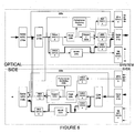
- FIGURE 6 there is illustrated a block diagram of the transceiver of FIGURE 2 configured for serial Gigabit Ethernet on the optical side and serial Gigabit Ethernet on the system side.
- Serial interface 215b Data is received from the system side at serial interface 215b.
- the serial interface 215b provides the data to CDR 219b.
- the CDR 219b recovers the data and a clock signal and provides the data and clock signal to demultiplexer 240(3)b.
- the demultiplexer 240(3)b deserializes the data signal resulting in 10 bit words.
- the 10-bit words bypass the 8b10b encoder/decoder unit 230b and are transmitted to multiplexer 235(2)b.
- the multiplexer 235(2)b is a 10:1 MUX which serializes the encoded signal and provides the serialized encoded signal to the serial interface 210b.
- the serial interface 210b outputs the serialized encoded Gigabit Ethernet signal to the optical side.
- the transceiver module 120 receives data from the optical side at the ingress path at serial interface 210a.
- the serial interface 210a provides the received data to a CDR 219a.
- the CDR 219a recovers the data and provides a clock signal to demultiplexer 240(2)a.
- the demultiplexer 240(2)a is a 1:10 demultiplexer which converts the received data to 10-bit words.
- the 10-bit words bypass the 8b10b encoder/decoder unit 230a and are transmitted to multiplexer 235(3)a.
- the multiplexer 235(3)a serializes the signal and provides the serialized signal to the serial interface 215a.
- the serial interface 215a outputs the data signal in accordance with the serial Gigabit Ethernet standard.
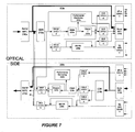
- FIGURE 7 there is illustrated a block diagram of the transceiver of FIGURE 2, configured to operate in a bypass mode.
- the bypass mode data is received from the system side at the serial interface 215b and transmitted directly to the optical side via serial interface 210b.
- Data received from the optical side is received at serial interface 210a and transmitted directly to serial interface 215a.
- the bypass mode can be used with any rate.
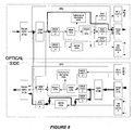
- FIGURE 8 there is illustrated a block diagram of the transceiver of FIGURE 2, configured to operate in a Gigabit Ethernet retimed mode.
- data is received from the system at the system interface 215b and provided to the CDR 219b.
- the CDR 219b provides the requisite retiming and outputs the data to the optical side via demultiplexer 240(3)b, bypassing encoder/decoder module 230b, to multiplexer 235(2)b, and serial interface 210b.
- Data received from the optical side is received at serial interface 210a and provided to CDR 219a.
- the CDR 219a provides the requisite retiming and transmits the data directly to the serial interface 215a.
- the serial interface 215a transmits the data to the system side.
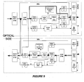
- FIGURE 9 there is illustrated a block diagram of the transceiver of FIGURE 2, configured to operate in a SONET retimed mode.
- data is received from the system side at the serial interface 215b.
- the serial interface 215b provides the data to a CDR 219b.
- the CDR 219b recovers the data and provides a clock signal to demultiplexer 240(2)b.
- the demultiplexer 240(2)b is a 1:16 DEMUX which deserializes the input signal, thereby resulting in 16-bit words.
- the 16 bit words are provided to a framer 228b.
- the framer 228b generates frames which are provided to the mapper 225b.
- the mapper 225b maps the frames to 16-bit words at 155.5 MHz, thereby resulting in 2.488 Gbps, or OC-48.
- the signal from the mapper 225b is provided to a 16:1 multiplexer 235(1)b and serial interface 210b.
- Serial interface 210a Data received from the optical side is received at serial interface 210a and provided to CDR 219a.
- the CDR 219a provides the requisite retiming and transmits the data directly to the serial interface 215a.
- the serial interface 215a transmits the data to the system side.
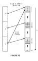
- FIGURE 10 there is a block diagram of OC-3 data mapped onto 16-bit wide data words at 155 MHz in accordance with STS-48.
- the OC-3 data comprises time slots 1,2,3, while the STS-48 comprises time slots, 1...48.
- the data from OC-3 time slot 1 is mapped to STS-48 time slot 1.
- the data from OC-3 time slot 2 is mapped to STS-48 time slot 17.
- the data from OC-3 time slot 3 is mapped to STS-48 time slots 7 and 33.
- the remaining STS-48 time slots are filled with 0's or null data.
- FIGURE 11 there is a block diagram of OC-12 data mapped onto 16-bit wide data words at 155 MHz in accordance with STS-48.
- the OC-12 data comprises time slots, 1...12.
- the time slots, 1...12 are staggered in order.
- the staggered ordering begins with time slot 1, and is then ordered with every third time slot following, e.g., 4, 7, and 10.
- the staggered ordering then continues with time slot 2 followed by every third time slot, e.g., 5, 8, and 11.
- the staggered ordering then continues with time slot 3 followed by every third time slot, e.g., 6, 9, and 12.
- the STS-48 data includes 48 time slots which are similarly staggered, e.g., 1, 4, 7, 10,...46, followed by 2, 5, 8, hence47, and 3, 6, 9, «48.
- the data from each OC-12 time slot n is mapped to the corresponding STS-48 time slot n.
- the remaining STS-48 time slots are filled with 0's or null data.
- the transceiver 120 as described herein may be implemented as a board level product, as a single chip, application specific integrated circuit (ASIC), or with varying levels of the transceiver 120 integrated on a single chip with other portions of the system as separate components.
- ASIC application specific integrated circuit
- the degree of integration of the monitoring system will primarily be determined by the data speeds, and cost considerations. Because of the sophisticated nature of modern processors, it is possible to utilize a commercially available processor, which may be implemented external to an ASIC implementation of the present system. Alternatively, if the processor is available as an ASIC core or logic block, then the commercially available processor can be implemented as part of an ASIC device.
Landscapes
- Engineering & Computer Science (AREA)
- Computer Networks & Wireless Communication (AREA)
- Signal Processing (AREA)
- Time-Division Multiplex Systems (AREA)
- Communication Control (AREA)
Applications Claiming Priority (4)
| Application Number | Priority Date | Filing Date | Title |
|---|---|---|---|
| US42307002P | 2002-11-01 | 2002-11-01 | |
| US423070P | 2002-11-01 | ||
| US355472 | 2003-01-31 | ||
| US10/355,472 US7324548B2 (en) | 2002-11-01 | 2003-01-31 | Transceiver system and method supporting variable rates and multiple protocols |
Publications (3)
| Publication Number | Publication Date |
|---|---|
| EP1416656A2 true EP1416656A2 (de) | 2004-05-06 |
| EP1416656A3 EP1416656A3 (de) | 2004-10-06 |
| EP1416656B1 EP1416656B1 (de) | 2014-01-08 |
Family
ID=32095755
Family Applications (1)
| Application Number | Title | Priority Date | Filing Date |
|---|---|---|---|
| EP20030023973 Expired - Lifetime EP1416656B1 (de) | 2002-11-01 | 2003-10-22 | Verfahren und Sende-Empfänger-Vorrichtung zur Unterstützung veränderlicher Bitraten und mehrerer Protokolle |
Country Status (1)
| Country | Link |
|---|---|
| EP (1) | EP1416656B1 (de) |
Cited By (2)
| Publication number | Priority date | Publication date | Assignee | Title |
|---|---|---|---|---|
| WO2005018120A1 (en) * | 2003-08-12 | 2005-02-24 | Teknovus, Inc. | Method and apparatus for multiplexing ethernet channels |
| USRE45557E1 (en) | 2002-11-01 | 2015-06-09 | Broadcom Corporation | Configurable voltage controlled oscillator system and method including dividing forming a portion of two or more divider paths |
Citations (2)
| Publication number | Priority date | Publication date | Assignee | Title |
|---|---|---|---|---|
| US5959749A (en) | 1998-05-20 | 1999-09-28 | Nortel Networks Corporation | Optical add/drop multiplexer/demultiplexer |
| US20010014104A1 (en) | 2000-02-09 | 2001-08-16 | Bottorff Paul A. | 10 Gigabit ethernet mappings for a common LAN/WAN PMD interface with a simple universal physical medium dependent interface |
Family Cites Families (1)
| Publication number | Priority date | Publication date | Assignee | Title |
|---|---|---|---|---|
| US7002986B1 (en) * | 1999-07-08 | 2006-02-21 | Nortel Networks Limited | Mapping arbitrary signals into SONET |
-
2003
- 2003-10-22 EP EP20030023973 patent/EP1416656B1/de not_active Expired - Lifetime
Patent Citations (2)
| Publication number | Priority date | Publication date | Assignee | Title |
|---|---|---|---|---|
| US5959749A (en) | 1998-05-20 | 1999-09-28 | Nortel Networks Corporation | Optical add/drop multiplexer/demultiplexer |
| US20010014104A1 (en) | 2000-02-09 | 2001-08-16 | Bottorff Paul A. | 10 Gigabit ethernet mappings for a common LAN/WAN PMD interface with a simple universal physical medium dependent interface |
Cited By (4)
| Publication number | Priority date | Publication date | Assignee | Title |
|---|---|---|---|---|
| USRE45557E1 (en) | 2002-11-01 | 2015-06-09 | Broadcom Corporation | Configurable voltage controlled oscillator system and method including dividing forming a portion of two or more divider paths |
| WO2005018120A1 (en) * | 2003-08-12 | 2005-02-24 | Teknovus, Inc. | Method and apparatus for multiplexing ethernet channels |
| US8483246B2 (en) | 2003-08-12 | 2013-07-09 | Broadcom Corporation | Method and apparatus for multiplexing Ethernet channels |
| US9264163B2 (en) | 2003-08-12 | 2016-02-16 | Broadcom Corporation | Method and apparatus for multiplexing ethernet channels |
Also Published As
| Publication number | Publication date |
|---|---|
| EP1416656A3 (de) | 2004-10-06 |
| EP1416656B1 (de) | 2014-01-08 |
Similar Documents
| Publication | Publication Date | Title |
|---|---|---|
| US20080130679A1 (en) | Transceiver system and method supporting variable rates and multiple protocols | |
| US5926303A (en) | System and apparatus for optical fiber interface | |
| US7436824B2 (en) | Distributed switch architecture including a growth input/output bus structure | |
| US5365510A (en) | Communications system with a single protection loop | |
| CN1083186C (zh) | 用于终接并产生同步传输信号的处理器装置 | |
| CA2304118C (en) | Protocol independent sub-rate device | |
| US20030193972A1 (en) | Redundant add/drop multiplexor | |
| US7130276B2 (en) | Hybrid time division multiplexing and data transport | |
| US20080232818A1 (en) | Interface board and optical transmission equipment | |
| WO2005002110A2 (en) | Multi-rate, multi-protocol, multi-port line interface for a multiservice switching platform | |
| US6122249A (en) | Add-drop multiplexing apparatus | |
| JPH07254890A (ja) | 光双方向伝送制御方式 | |
| US5754545A (en) | Add-drop multiplexer with enhancement of accessibility to signals in different hierarchical levels and flexibility in various services and circuit setting operations | |
| US6487223B1 (en) | SDH transmission apparatus with flexible system configuration | |
| US7359410B2 (en) | Apparatus and method for increasing optical density of SONET multiplexer using integral components | |
| US7379481B2 (en) | Apparatus and method for automatic provisioning of SONET multiplexer | |
| US7526197B2 (en) | Utilizing the protecting bandwidth in a SONET network | |
| US7447429B2 (en) | Bidirectional line switched ring network | |
| EP1416656A2 (de) | Verfahren und Sende-Empfänger-Vorrichtung zur Unterstützung veränderlicher Bitraten und mehrerer Protokolle | |
| US8160109B2 (en) | Method and system for synchronizing a transceiver and a downstream device in an optical transmission network | |
| US7145922B2 (en) | Composite add/drop multiplexor with crisscross loop back | |
| US7583599B1 (en) | Transporting stream client signals via packet interface using GFP mapping | |
| US7356076B2 (en) | System and method supporting auto-recovery in a transceiver system | |
| US6735197B1 (en) | Concatenation detection across multiple chips | |
| JP3742586B2 (ja) | 伝送装置及びインタフェース装置 |
Legal Events
| Date | Code | Title | Description |
|---|---|---|---|
| PUAI | Public reference made under article 153(3) epc to a published international application that has entered the european phase |
Free format text: ORIGINAL CODE: 0009012 |
|
| AK | Designated contracting states |
Kind code of ref document: A2 Designated state(s): AT BE BG CH CY CZ DE DK EE ES FI FR GB GR HU IE IT LI LU MC NL PT RO SE SI SK TR |
|
| AX | Request for extension of the european patent |
Extension state: AL LT LV MK |
|
| PUAL | Search report despatched |
Free format text: ORIGINAL CODE: 0009013 |
|
| AK | Designated contracting states |
Kind code of ref document: A3 Designated state(s): AT BE BG CH CY CZ DE DK EE ES FI FR GB GR HU IE IT LI LU MC NL PT RO SE SI SK TR |
|
| AX | Request for extension of the european patent |
Extension state: AL LT LV MK |
|
| 17P | Request for examination filed |
Effective date: 20050406 |
|
| AKX | Designation fees paid |
Designated state(s): DE FR GB |
|
| 17Q | First examination report despatched |
Effective date: 20070321 |
|
| RAP1 | Party data changed (applicant data changed or rights of an application transferred) |
Owner name: BROADCOM CORPORATION |
|
| GRAP | Despatch of communication of intention to grant a patent |
Free format text: ORIGINAL CODE: EPIDOSNIGR1 |
|
| INTG | Intention to grant announced |
Effective date: 20130723 |
|
| GRAS | Grant fee paid |
Free format text: ORIGINAL CODE: EPIDOSNIGR3 |
|
| GRAA | (expected) grant |
Free format text: ORIGINAL CODE: 0009210 |
|
| AK | Designated contracting states |
Kind code of ref document: B1 Designated state(s): DE FR GB |
|
| REG | Reference to a national code |
Ref country code: GB Ref legal event code: FG4D |
|
| REG | Reference to a national code |
Ref country code: DE Ref legal event code: R096 Ref document number: 60345567 Country of ref document: DE Effective date: 20140220 |
|
| REG | Reference to a national code |
Ref country code: DE Ref legal event code: R097 Ref document number: 60345567 Country of ref document: DE |
|
| PLBE | No opposition filed within time limit |
Free format text: ORIGINAL CODE: 0009261 |
|
| STAA | Information on the status of an ep patent application or granted ep patent |
Free format text: STATUS: NO OPPOSITION FILED WITHIN TIME LIMIT |
|
| 26N | No opposition filed |
Effective date: 20141009 |
|
| REG | Reference to a national code |
Ref country code: DE Ref legal event code: R097 Ref document number: 60345567 Country of ref document: DE Effective date: 20141009 |
|
| GBPC | Gb: european patent ceased through non-payment of renewal fee |
Effective date: 20141022 |
|
| PG25 | Lapsed in a contracting state [announced via postgrant information from national office to epo] |
Ref country code: GB Free format text: LAPSE BECAUSE OF NON-PAYMENT OF DUE FEES Effective date: 20141022 |
|
| REG | Reference to a national code |
Ref country code: FR Ref legal event code: ST Effective date: 20150630 |
|
| PG25 | Lapsed in a contracting state [announced via postgrant information from national office to epo] |
Ref country code: FR Free format text: LAPSE BECAUSE OF NON-PAYMENT OF DUE FEES Effective date: 20141031 |
|
| REG | Reference to a national code |
Ref country code: DE Ref legal event code: R082 Ref document number: 60345567 Country of ref document: DE Representative=s name: BOSCH JEHLE PATENTANWALTSGESELLSCHAFT MBH, DE Ref country code: DE Ref legal event code: R081 Ref document number: 60345567 Country of ref document: DE Owner name: AVAGO TECHNOLOGIES INTERNATIONAL SALES PTE. LT, SG Free format text: FORMER OWNER: BROADCOM CORP., IRVINE, CALIF., US Ref country code: DE Ref legal event code: R081 Ref document number: 60345567 Country of ref document: DE Owner name: AVAGO TECHNOLOGIES GENERAL IP (SINGAPORE) PTE., SG Free format text: FORMER OWNER: BROADCOM CORP., IRVINE, CALIF., US |
|
| REG | Reference to a national code |
Ref country code: DE Ref legal event code: R081 Ref document number: 60345567 Country of ref document: DE Owner name: AVAGO TECHNOLOGIES INTERNATIONAL SALES PTE. LT, SG Free format text: FORMER OWNER: AVAGO TECHNOLOGIES GENERAL IP (SINGAPORE) PTE. LTD., SINGAPORE, SG Ref country code: DE Ref legal event code: R082 Ref document number: 60345567 Country of ref document: DE Representative=s name: BOSCH JEHLE PATENTANWALTSGESELLSCHAFT MBH, DE |
|
| PGFP | Annual fee paid to national office [announced via postgrant information from national office to epo] |
Ref country code: DE Payment date: 20220616 Year of fee payment: 20 |
|
| REG | Reference to a national code |
Ref country code: DE Ref legal event code: R071 Ref document number: 60345567 Country of ref document: DE |