EP1416524A2 - Method of planarizing a semiconductor die - Google Patents
Method of planarizing a semiconductor die Download PDFInfo
- Publication number
- EP1416524A2 EP1416524A2 EP03256830A EP03256830A EP1416524A2 EP 1416524 A2 EP1416524 A2 EP 1416524A2 EP 03256830 A EP03256830 A EP 03256830A EP 03256830 A EP03256830 A EP 03256830A EP 1416524 A2 EP1416524 A2 EP 1416524A2
- Authority
- EP
- European Patent Office
- Prior art keywords
- layer
- gap
- wafer
- pillar
- silicon dioxide
- Prior art date
- Legal status (The legal status is an assumption and is not a legal conclusion. Google has not performed a legal analysis and makes no representation as to the accuracy of the status listed.)
- Withdrawn
Links
Images



Classifications
-
- H—ELECTRICITY
- H10—SEMICONDUCTOR DEVICES; ELECTRIC SOLID-STATE DEVICES NOT OTHERWISE PROVIDED FOR
- H10P—GENERIC PROCESSES OR APPARATUS FOR THE MANUFACTURE OR TREATMENT OF DEVICES COVERED BY CLASS H10
- H10P52/00—Grinding, lapping or polishing of wafers, substrates or parts of devices
-
- H—ELECTRICITY
- H10—SEMICONDUCTOR DEVICES; ELECTRIC SOLID-STATE DEVICES NOT OTHERWISE PROVIDED FOR
- H10P—GENERIC PROCESSES OR APPARATUS FOR THE MANUFACTURE OR TREATMENT OF DEVICES COVERED BY CLASS H10
- H10P95/00—Generic processes or apparatus for manufacture or treatments not covered by the other groups of this subclass
- H10P95/06—Planarisation of inorganic insulating materials
- H10P95/062—Planarisation of inorganic insulating materials involving a dielectric removal step
- H10P95/064—Planarisation of inorganic insulating materials involving a dielectric removal step the removal being chemical etching
-
- H—ELECTRICITY
- H10—SEMICONDUCTOR DEVICES; ELECTRIC SOLID-STATE DEVICES NOT OTHERWISE PROVIDED FOR
- H10P—GENERIC PROCESSES OR APPARATUS FOR THE MANUFACTURE OR TREATMENT OF DEVICES COVERED BY CLASS H10
- H10P95/00—Generic processes or apparatus for manufacture or treatments not covered by the other groups of this subclass
- H10P95/06—Planarisation of inorganic insulating materials
- H10P95/062—Planarisation of inorganic insulating materials involving a dielectric removal step
Definitions
- the present invention relates to a method of planarizing a layer of a first material, and more particularly a dieletric layer, using chemical mechanical polishing techniques on a semiconductor die.
- CMP Chemical mechanical polishing
- the material to be planarized is a dieletric, such as silicon dioxide, which has been deposited on another dieletric such as silicon nitride.
- the silicon nitride has a top planar surface with the silicon dioxide deposited thereon.
- the silicon dioxide deposited on the silicon nitride will flow through the holes in the silicon nitride into the trenches in the substrate, thereby causing an uneven level above the top planar surface of the silicon nitride.
- the height of the silicon dioxide above the top planar surface of the silicon nitride can vary substantially.
- One prior art method to attempt to level the silicon dioxide is to create artificial dummy diffusion regions in the substrate of large field areas and filling it with oxide, but this does not address the large active areas and CMP's dishing effect associated with the large active areas. In other words, this method alone does not address the problem of the planarization of all the areas of the wafer.
- Another prior art solution is to mask certain portions of the silicon dioxide where the height of the silicon dioxide above the top planar surface of the silicon-nitride is substantial. The silicon dioxide in the masked portion is removed thereby removing a substantial portion of the silicon dioxide in the portion where the height of the silicon dioxide above the top planar surface is substantial. This, however, creates a well-known undesired effect called "dishing" wherein polishing of the silicon dioxide causes the removal of silicon nitride in certain areas.
- a method of planarizing a first material on a second material of a semiconductor die is disclosed.
- a plurality of substantially identical semiconductor dies are defined on a semiconductor wafer with the wafer having a planar surface.
- the plurality of dies are separated from one another by a scribe line.
- a layer of the second material is formed on the planar surface of the semiconductor wafer, wherein the layer of the second material has a top surface which is substantially parallel to the planar surface.
- a layer of the first material is on the top surface and the layer of the first material varies in a height direction above the top surface.
- a mask is formed across the wafer, where the mask has a plurality of locations with each location having differing density of gap-to-pillar ratio, which is proportional to the height of the first material above the top surface.
- the first material is anisotropically etched through each gap of the mask across the entire wafer wherein each gap is etched by the same amount in the height direction.
- CMP is then used to planarize the first material to the top surface across the wafer.
- Fig. 1 is a top view of a wafer having a plurality of substantially identical semiconductor dies defined thereon and having a first material thereon to be planarized in accordance with the method of the present invention.
- Fig. 2 is a partial cross-sectional view of one semiconductor die shown in Fig. 1 of an exemplar profile of the silicon dioxide which is grown on silicon nitride and is desired to be planarized.
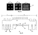
- Fig. 3A is a top view of one method of the present invention using a mask in which a field has a plurality of pillars with different sizes but with the gaps between adjacent pillars all being the same size.
- Fig. 3B is a cross-sectional view of the mask pattern using the mask shown in Fig. 3A on the structure shown in Fig. 2.
- Fig. 3C is a cross-sectional view of the structure shown in Fig. 3B after the mask has been applied and etched.
- Fig. 4A is a top view of another method of the present invention using a mask in which a field has a plurality of pillars with the same size but with the gaps between adjacent pillars all being different.
- Fig. 4B is a cross-sectional view of the mask pattern using the mask shown in Fig. 4A on the structure shown in Fig. 2.
- Fig. 4C is a cross-sectional view of the structure shown in Fig. 4B after the mask has been applied and etched.
- a top view of a wafer 10 of a semiconductor substrate is single crystalline silicon or it may be a composite semiconductor, such as a III-V material.
- the wafer 10 has defined thereon a plurality of substantially identical semiconductor dies 12, with each die 12 separated from one another by a scribe line 14.
- the wafer 10 is characterized by having a substantially planar top surface 16.
- a thin layer 20 of silicon dioxide is deposited or thermally grown on this top surface 16 of the substrate 10.
- the layer 20 of silicon dioxide can be, although not necessarily, used as the gate oxide for MOS transistors and the like.
- Deposited on the first layer 20 of silicon dioxide is a layer 22 of silicon nitride.
- the silicon nitride has a planar surface 24, which is substantially parallel to the top surface 16 of the semiconductor substrate 10.
- trenches 26(a-c) are etched into the silicon nitride 22 and through the silicon dioxide 20 and into the silicon substrate 10.
- a layer of silicon dioxide 28 fills the trenches 26(a-c) and is also deposited on top of the planar surface 24 on the silicon nitride 22.
- the layer 28 of silicon dioxide is deposited by HDP (high density plasma) deposition. The silicon dioxide 28 is deposited on the planar surface 24 of the silicon nitride 22 and into the trenches 26(a-c) but does not form a planar surface which is parallel to the planar surface 24.
- the thickness of the silicon dioxide 28 above the planar surface 24 of the silicon nitride 22 will vary.
- An exemplary cross-sectional view of a die 12 is shown in Fig. 2.
- the layer 20 of silicon dioxide, layer 22 of silicon nitride, and layer 28 of silicon nitride is applied across the entire wafer 10, including over the scribe lines 14.
- this does not mean that layers 20 and 22 are everywhere on the top surface 16 of the substrate 10.
- a mask is first applied to the contour of the silicon dioxide 28.
- the mask comprises a plurality of substantially identical fields 30, which are shown in Fig. 3A.
- Each of the fields 30 is substantially identical or congruent.
- a pillar 32 is a cross-sectional area and in the preferred embodiment, it is substantially square in shape.
- a gap is defined as the distance from the center of a pillar 32 to the center of an adjacent pillar 32.
- the gap distance X is the same for each of the three fields 30 shown in Fig. 3A.
- a mask is formed comprising of a plurality of congruent fields 30, each having one or more pillars 32 that have different sizes, but with gaps all of the same size.
- the size of each pillar i.e., the cross-sectional dimension of the pillar 32, is dependent upon the thickness of the silicon dioxide 28 above the planar surface 24 upon which the fields 30 are placed.
- the structure therein has two regions designated "A" and "B.”
- the thickness or the amount of silicon dioxide 28 which is on the planar surface 24 of the silicon nitride 22, is substantially less than the thickness of the silicon dioxide 28 in the region designated "B."
- This variation in the thickness of the silicon dioxide 28 would cause an inverse variation in the density of pillar-to-gap ratio that is formed on the silicon dioxide 28.
- the thickness is small, as in region A, the density of pillar-to-gap ratio is large in comparison to region B, where the thickness of the silicon dioxide 28 is large and density of pillar-to-gap ratio is small.
- the thickness at each region can be calculated based upon the anticipated thickness due to the number of trenches in the selected region. For example, since in region A there are two trenches 26a and 26b, whose depths are known, it can be calculated what the ultimate thickness of the silicon dioxide 28 in region A would be due to a portion of the silicon dioxide 28 in that region A used to fill the trenches 26a and 26b, thereby lowering the height of the silicon dioxide 28 in region A.
- the calculations can be made based upon the size of the trench 26c and the volume of silicon dioxide which would flow to fill the trench 26c thereby lowering the height of the silicon dioxide 28 in that region.
- a computer can be used to calculate the height or thickness of the silicon dioxide 28 in various regions and therefore to calculate the density of the pillar-to-gap ratio in those regions.
- the computer must know the information of the pattern layout on the mask used to etch the trenches as well as the depth of the trench plus the thickness of the layers 20 and 22.
- an anisotropic etch is performed.
- the silicon dioxide 28 between gaps which are the regions between adjacent pillars 32 which are formed on the contour of the silicon dioxide 28 is anisotropically etched.
- Each gap is etched into the silicon dioxide 28 by the same thickness amount Y.
- the resultant structure is shown in Fig. 3C.
- the wafer 10 with the structure shown in Fig. 3C is then subject to a conventional CMP polishing method.
- the silicon dioxide 28 would reach the planar surface 24 of the structure.
- Fig. 4A there is shown another method of the present invention.
- the fields 30 are congruent and of the same size.
- one or more pillars 32 of the same size are formed in each field 30, with the gap between each pillar being different.
- the density of the pillar 30 to the gap would depend upon the "height" of the silicon dioxide 28 upon which the fields are fixed, plus the thickness of layers 20 and 22.
- a mask in which the fields 30 are placed on the contour of the silicon dioxide 28 is formed, resulting in the formation of a number of regions in which within each region the fields are congruent but the pillar-to-gap ratio differs.
- the silicon dioxide 28 between adjacent pillars or in the gaps are anisotropically etched.
- the silicon dioxide 28 is anisotropically etched by the same amount Y in the "height" direction, resulting in the structure shown in Fig. 4C.
- the structure shown in Fig. 4C is then CMP polished and the resultant structure would be the silicon dioxide 28 being substantially planar to the planar surface 24 of the silicon nitride 22.
- the theory of the present invention is as follows.
- a subsequent CMP polishing step would cause those fields that have low density to be etch or polished faster than those fields having high density.
- the fields having low density represent those fields that are over portions of the silicon dioxide that are thick. Therefore, those regions will be etched faster than the regions where the silicon dioxide is 'thin". Further polishing eventually brings both portions into the same planar field.
- the etch rate in a CUT process having a certain topography with density D is R/D, where R is the etch rate of a flat surface.
- the density D is equal to the total area of high feature (total area of pillars 32)/ divided by Total area (area of field) or (total area of pillars 32 + total area of gaps).
- density D will always be less than or equal to 1.0. If the density is low, i.e. there is less amount of pillars, then the etch rate will be faster than if the density is high. Since density low represents the density of the mask over the region of the silicon dioxide which is thicker than the region of the silicon dioxide that is thinner, the thicker regions will be etched faster.
- the size of a field can be of microscopic size, e.g. 50 um by 50um.
Landscapes
- Element Separation (AREA)
- Mechanical Treatment Of Semiconductor (AREA)
- Internal Circuitry In Semiconductor Integrated Circuit Devices (AREA)
- Drying Of Semiconductors (AREA)
Abstract
Description
Claims (15)
- A method of chemical mechanical polishing (CMP) a first material on a second material of a semiconductor die, said method comprising:defining a plurality of substantially identical semiconductor dies on a semiconductor wafer, said wafer having a planar surface, and wherein said plurality of dies are separated from one another by a scribe line;forming a layer of said second material on said planar surface wherein said layer of said second material having a top surface, substantially parallel to said planar surface;forming a layer of said first material on said top surface, wherein said layer of said first material varying in a height direction above said top surface;forming a mask across the wafer, wherein said mask having a plurality of locations with each location having differing density of gap to pillar ratio, which is proportional to the height of said first material above said top surface;anistropically etching said first material through each gap of said mask, across the wafer, wherein each gap is etched by the same amount in the height direction; andusing CMP to planarize said first material to said top surface across the wafer.
- The method of claim 1 wherein said layer of second material is silicon nitride, and wherein said layer of first material is silicon dioxide.
- The method of claim 1 further comprising a layer of third material between said layer of second material and said wafer.
- The method of claim 3 wherein said layer of second material is silicon nitride, and wherein said layer of first material and third material are silicon dioxide.
- The method of claim 4 wherein said layer of second material has holes therein connecting said layer of first material and third material.
- The method of claim 5 wherein each of said dies has trenches therein filled with said layer of first material.
- The method of claim 6 wherein said density of gap to pillar comprises a plurality of substantially congruent fields with each field having the same size pillar but different size gap.
- The method of claim 6 wherein said density of gap to pillar comprises a plurality of substantially congruent fields with each field having different size pillar but same size gap.
- The method of claim 1 wherein said density of gap to pillar comprises a plurality of substantially congruent fields with each field having the same size pillar but different size gap.
- The method of claim 1 wherein said density of gap to pillar comprises a plurality of substantially congruent fields with each field having different size pillar but same size gap.
- A method of planarizing a first material on a second material of a semiconductor die, said method comprising:defining a plurality of substantially identical semiconductor dies on a semiconductor wafer, said wafer having a planar surface, and wherein said plurality of dies are separated from one another by a scribe line;forming a layer of a third material on said planar surface;forming a layer of said second material on said layer of third material, said layer of said second material having a top surface substantially parallel to said planar surface;masking selective portions of said layer of second material, with other portions of said layer of second material unmasked;etching said layer of second material, said layer of first material, and said semiconductor wafer to form trenches therein, through said other portions unmasked;applying said layer of said first material on said wafer, including in said trenches and on said second material, wherein said layer of said first material varying in a height direction above said top surface;forming a mask across the wafer, wherein said mask having a plurality of locations with each location having differing density of gap to pillar ratio which is proportional to the amount of said first material in the height direction from said top surface at said location;anistropically etching said first material through each gap of said mask, across the wafer, wherein each gap is etched by the same amount in the height direction; andusing CMP to planarize said first material to said top surface across the wafer.
- The method of claim 11, wherein said masking step further comprises:forming a mask covering select portions of said layer of second material with other portions unmasked; andremoving said mask after said etching step.
- The method of claim 12 wherein said first material and said third material is silicon dioxide, and said second material is silicon nitride.
- The method of claim 12 wherein said density of gap to pillar comprises a plurality of substantially congruent fields with each field having the same size pillar but different size gap.
- The method of claim 12 wherein said density of gap to pillar comprises a plurality of substantially congruent fields with each field having different size pillar but same size gap.
Applications Claiming Priority (4)
| Application Number | Priority Date | Filing Date | Title |
|---|---|---|---|
| US42231402P | 2002-10-29 | 2002-10-29 | |
| US422314P | 2002-10-29 | ||
| US10/423,270 US6703318B1 (en) | 2002-10-29 | 2003-04-25 | Method of planarizing a semiconductor die |
| US423270 | 2003-04-25 |
Publications (2)
| Publication Number | Publication Date |
|---|---|
| EP1416524A2 true EP1416524A2 (en) | 2004-05-06 |
| EP1416524A3 EP1416524A3 (en) | 2005-09-21 |
Family
ID=31891557
Family Applications (1)
| Application Number | Title | Priority Date | Filing Date |
|---|---|---|---|
| EP03256830A Withdrawn EP1416524A3 (en) | 2002-10-29 | 2003-10-29 | Method of planarizing a semiconductor die |
Country Status (6)
| Country | Link |
|---|---|
| US (2) | US6703318B1 (en) |
| EP (1) | EP1416524A3 (en) |
| JP (1) | JP4573515B2 (en) |
| KR (1) | KR20040038788A (en) |
| CN (1) | CN100416770C (en) |
| TW (1) | TWI320584B (en) |
Families Citing this family (9)
| Publication number | Priority date | Publication date | Assignee | Title |
|---|---|---|---|---|
| US7522091B2 (en) * | 2002-07-15 | 2009-04-21 | Automotive Systems Laboratory, Inc. | Road curvature estimation system |
| US20110151190A1 (en) * | 2007-05-08 | 2011-06-23 | Jae-Hyun Chung | Shadow edge lithography for nanoscale patterning and manufacturing |
| KR100848461B1 (en) * | 2007-08-16 | 2008-07-25 | 주식회사 동부하이텍 | Manufacturing Method of Semiconductor Device |
| JP4968228B2 (en) * | 2007-11-07 | 2012-07-04 | マツダ株式会社 | Engine superstructure |
| US8551886B2 (en) * | 2007-12-28 | 2013-10-08 | Texas Instruments Incorporated | CMP process for processing STI on two distinct silicon planes |
| JP5356742B2 (en) * | 2008-07-10 | 2013-12-04 | ラピスセミコンダクタ株式会社 | Semiconductor device, semiconductor device manufacturing method, and semiconductor package manufacturing method |
| US8129095B2 (en) * | 2009-04-08 | 2012-03-06 | International Business Machines Corporation | Methods, photomasks and methods of fabricating photomasks for improving damascene wire uniformity without reducing performance |
| CN103854967B (en) * | 2012-11-30 | 2017-09-22 | 中国科学院微电子研究所 | Planarization method |
| US9853149B1 (en) * | 2016-10-03 | 2017-12-26 | Taiwan Semiconductor Manufacturing Co., Ltd. | Floating grid and crown-shaping poly for improving ILD CMP dishing |
Family Cites Families (15)
| Publication number | Priority date | Publication date | Assignee | Title |
|---|---|---|---|---|
| US5928960A (en) * | 1996-10-24 | 1999-07-27 | International Business Machines Corporation | Process for reducing pattern factor effects in CMP planarization |
| EP0855739A1 (en) * | 1997-01-24 | 1998-07-29 | Texas Instruments Inc. | Tapered dielectric etch process for moat etchback |
| US6025270A (en) * | 1997-02-03 | 2000-02-15 | Taiwan Semiconductor Manufacturing Company, Ltd. | Planarization process using tailored etchback and CMP |
| US5911110A (en) * | 1997-10-28 | 1999-06-08 | Taiwan Semiconductor Manufacturing Co., Ltd. | Method of forming shallow trench isolation with dummy pattern in reverse tone mask |
| JP3279276B2 (en) * | 1999-01-27 | 2002-04-30 | 日本電気株式会社 | Method for manufacturing semiconductor device |
| JP2001044168A (en) * | 1999-07-30 | 2001-02-16 | Matsushita Electronics Industry Corp | Manufacture of semiconductor device |
| JP4370484B2 (en) * | 1999-08-16 | 2009-11-25 | エルピーダメモリ株式会社 | Manufacturing method of semiconductor device |
| JP4347960B2 (en) | 1999-09-14 | 2009-10-21 | 株式会社ディスコ | Dicing method |
| JP3344397B2 (en) * | 2000-01-21 | 2002-11-11 | 日本電気株式会社 | Method for manufacturing semiconductor device |
| JP2001326199A (en) * | 2000-05-17 | 2001-11-22 | Hitachi Ltd | Method for manufacturing semiconductor integrated circuit device |
| JP2002026199A (en) * | 2000-07-06 | 2002-01-25 | Nakamura Seisakusho Kk | Method of forming heat dissipating member for electronic component |
| JP2002026119A (en) * | 2000-07-10 | 2002-01-25 | Sharp Corp | Method for manufacturing semiconductor device |
| JP2002270769A (en) * | 2001-03-08 | 2002-09-20 | Toshiba Corp | Semiconductor device and manufacturing method thereof |
| JP2002270688A (en) * | 2001-03-09 | 2002-09-20 | Oki Electric Ind Co Ltd | A method for manufacturing a semiconductor device. |
| US6541324B1 (en) | 2001-11-02 | 2003-04-01 | Silicon Storage Technology, Inc. | Method of forming a semiconductor array of floating gate memory cells having strap regions and a peripheral logic device region |
-
2003
- 2003-04-25 US US10/423,270 patent/US6703318B1/en not_active Expired - Lifetime
- 2003-10-23 TW TW092129461A patent/TWI320584B/en not_active IP Right Cessation
- 2003-10-29 KR KR1020030075909A patent/KR20040038788A/en not_active Ceased
- 2003-10-29 JP JP2003368772A patent/JP4573515B2/en not_active Expired - Fee Related
- 2003-10-29 CN CNB2003101046146A patent/CN100416770C/en not_active Expired - Fee Related
- 2003-10-29 EP EP03256830A patent/EP1416524A3/en not_active Withdrawn
-
2004
- 2004-01-21 US US10/762,807 patent/US6969687B2/en not_active Expired - Lifetime
Also Published As
| Publication number | Publication date |
|---|---|
| JP2004153276A (en) | 2004-05-27 |
| US20040152397A1 (en) | 2004-08-05 |
| US6703318B1 (en) | 2004-03-09 |
| CN1499581A (en) | 2004-05-26 |
| JP4573515B2 (en) | 2010-11-04 |
| TW200415719A (en) | 2004-08-16 |
| TWI320584B (en) | 2010-02-11 |
| KR20040038788A (en) | 2004-05-08 |
| US6969687B2 (en) | 2005-11-29 |
| CN100416770C (en) | 2008-09-03 |
| EP1416524A3 (en) | 2005-09-21 |
Similar Documents
| Publication | Publication Date | Title |
|---|---|---|
| US5302233A (en) | Method for shaping features of a semiconductor structure using chemical mechanical planarization (CMP) | |
| US6805614B2 (en) | Multilayered CMP stop for flat planarization | |
| US9799727B2 (en) | Isolation trench fill using oxide liner and nitride etch back technique with dual trench depth capability | |
| CN1099133C (en) | Gapfill and planarization process for shallow trench isolation | |
| JPS6242445A (en) | Integrated circuit and manufacture thereof | |
| US6703318B1 (en) | Method of planarizing a semiconductor die | |
| TWI336116B (en) | Trench isolation structure for a semiconductor device with a different degree of corner rounding and a method of manufacturing the same | |
| EP0954023A1 (en) | Isolation trench fabrication process | |
| EP1347509A2 (en) | Method to improve sti nano gap fill and moat nitride pull back | |
| US6627492B2 (en) | Methods of forming polished material and methods of forming isolation regions | |
| US6794268B2 (en) | Fabricating deeper and shallower trenches in semiconductor structures | |
| US6380047B1 (en) | Shallow trench isolation formation with two source/drain masks and simplified planarization mask | |
| CN120834005A (en) | Semiconductor structure and manufacturing method thereof, and electronic device | |
| CN101246884B (en) | Shallow plough groove isolation region, shallow plough groove isolation region mask plate and its production method | |
| KR100408864B1 (en) | Method of forming a device isolation film in a semiconductor device | |
| JP2002208630A (en) | Method for manufacturing semiconductor device | |
| US20020123207A1 (en) | Methods of manufacturing semiconductor devices | |
| KR100317716B1 (en) | Method of isolating between devices with trench | |
| Zelenak | Chemical Mechanical Pad Characterization Using Shallow Trench Isolation Structures | |
| JP2001210710A (en) | Process for forming shallow trench isolation using sacrificial layer | |
| US6410402B1 (en) | Method of providing variant fills in semiconductor trenches | |
| TW442907B (en) | Forming method of shallow trench isolation filled up high-density plasma oxide layer | |
| US8551886B2 (en) | CMP process for processing STI on two distinct silicon planes | |
| JP2003152073A (en) | Method for manufacturing semiconductor device | |
| KR970018162A (en) | Manufacturing method of semiconductor device |
Legal Events
| Date | Code | Title | Description |
|---|---|---|---|
| PUAI | Public reference made under article 153(3) epc to a published international application that has entered the european phase |
Free format text: ORIGINAL CODE: 0009012 |
|
| AK | Designated contracting states |
Kind code of ref document: A2 Designated state(s): AT BE BG CH CY CZ DE DK EE ES FI FR GB GR HU IE IT LI LU MC NL PT RO SE SI SK TR |
|
| AX | Request for extension of the european patent |
Extension state: AL LT LV MK |
|
| RIN1 | Information on inventor provided before grant (corrected) |
Inventor name: SHARMA, GIAN Inventor name: LEVI, AMITAY |
|
| PUAL | Search report despatched |
Free format text: ORIGINAL CODE: 0009013 |
|
| AK | Designated contracting states |
Kind code of ref document: A3 Designated state(s): AT BE BG CH CY CZ DE DK EE ES FI FR GB GR HU IE IT LI LU MC NL PT RO SE SI SK TR |
|
| AX | Request for extension of the european patent |
Extension state: AL LT LV MK |
|
| RIC1 | Information provided on ipc code assigned before grant |
Ipc: 7H 01L 21/762 B Ipc: 7H 01L 21/3105 A |
|
| 17P | Request for examination filed |
Effective date: 20060321 |
|
| AKX | Designation fees paid |
Designated state(s): DE FR GB IT |
|
| 17Q | First examination report despatched |
Effective date: 20061129 |
|
| STAA | Information on the status of an ep patent application or granted ep patent |
Free format text: STATUS: THE APPLICATION HAS BEEN WITHDRAWN |
|
| 18W | Application withdrawn |
Effective date: 20090916 |