EP1413617A1 - Organic light-emitting device using iptycene derivatives - Google Patents
Organic light-emitting device using iptycene derivatives Download PDFInfo
- Publication number
- EP1413617A1 EP1413617A1 EP03255112A EP03255112A EP1413617A1 EP 1413617 A1 EP1413617 A1 EP 1413617A1 EP 03255112 A EP03255112 A EP 03255112A EP 03255112 A EP03255112 A EP 03255112A EP 1413617 A1 EP1413617 A1 EP 1413617A1
- Authority
- EP
- European Patent Office
- Prior art keywords
- emitting device
- organic light
- iptycene
- light emitting
- charge transport
- Prior art date
- Legal status (The legal status is an assumption and is not a legal conclusion. Google has not performed a legal analysis and makes no representation as to the accuracy of the status listed.)
- Withdrawn
Links
- 0 C*(c(cc1)ccc1-c1ccc(*(c2ccc(C3c4ccccc4C4c5ccccc35)c4c2)c2ccc(cccc3)c3c2)cc1)c1cc2ccccc2cc1 Chemical compound C*(c(cc1)ccc1-c1ccc(*(c2ccc(C3c4ccccc4C4c5ccccc35)c4c2)c2ccc(cccc3)c3c2)cc1)c1cc2ccccc2cc1 0.000 description 4
- QFESQSDROMKWED-UHFFFAOYSA-N Brc1cc(C(c2c(C34)cccc2)c2c3cccc2)c4cc1Br Chemical compound Brc1cc(C(c2c(C34)cccc2)c2c3cccc2)c4cc1Br QFESQSDROMKWED-UHFFFAOYSA-N 0.000 description 1
- ILHKZTGBAVBPAH-UHFFFAOYSA-N C(C1C2c3ccccc33)C=CC=C1C3c1c2c2cc3c(C4c5ccccc5C5c6c4cccc6)c5c(C4c5ccccc5C5c6c4cccc6)c5c3cc2c2c1C1c3ccccc3C2c2c1cccc2 Chemical compound C(C1C2c3ccccc33)C=CC=C1C3c1c2c2cc3c(C4c5ccccc5C5c6c4cccc6)c5c(C4c5ccccc5C5c6c4cccc6)c5c3cc2c2c1C1c3ccccc3C2c2c1cccc2 ILHKZTGBAVBPAH-UHFFFAOYSA-N 0.000 description 1
- SBTRSQOSNYAIIF-UHFFFAOYSA-N c1cc(C2c3ccccc3C3c4cc2ccc4-c(cc2)ccc2-c2nnc(-c(cc4)ccc4-c4cc(C5c6ccccc6C6c7c5cccc7)c6cc4)[o]2)c3cc1 Chemical compound c1cc(C2c3ccccc3C3c4cc2ccc4-c(cc2)ccc2-c2nnc(-c(cc4)ccc4-c4cc(C5c6ccccc6C6c7c5cccc7)c6cc4)[o]2)c3cc1 SBTRSQOSNYAIIF-UHFFFAOYSA-N 0.000 description 1
Classifications
-
- H—ELECTRICITY
- H10—SEMICONDUCTOR DEVICES; ELECTRIC SOLID-STATE DEVICES NOT OTHERWISE PROVIDED FOR
- H10K—ORGANIC ELECTRIC SOLID-STATE DEVICES
- H10K85/00—Organic materials used in the body or electrodes of devices covered by this subclass
- H10K85/60—Organic compounds having low molecular weight
- H10K85/615—Polycyclic condensed aromatic hydrocarbons, e.g. anthracene
-
- C—CHEMISTRY; METALLURGY
- C07—ORGANIC CHEMISTRY
- C07C—ACYCLIC OR CARBOCYCLIC COMPOUNDS
- C07C13/00—Cyclic hydrocarbons containing rings other than, or in addition to, six-membered aromatic rings
- C07C13/28—Polycyclic hydrocarbons or acyclic hydrocarbon derivatives thereof
- C07C13/32—Polycyclic hydrocarbons or acyclic hydrocarbon derivatives thereof with condensed rings
- C07C13/62—Polycyclic hydrocarbons or acyclic hydrocarbon derivatives thereof with condensed rings with more than three condensed rings
- C07C13/64—Polycyclic hydrocarbons or acyclic hydrocarbon derivatives thereof with condensed rings with more than three condensed rings with a bridged ring system
-
- C—CHEMISTRY; METALLURGY
- C09—DYES; PAINTS; POLISHES; NATURAL RESINS; ADHESIVES; COMPOSITIONS NOT OTHERWISE PROVIDED FOR; APPLICATIONS OF MATERIALS NOT OTHERWISE PROVIDED FOR
- C09K—MATERIALS FOR MISCELLANEOUS APPLICATIONS, NOT PROVIDED FOR ELSEWHERE
- C09K11/00—Luminescent, e.g. electroluminescent, chemiluminescent materials
- C09K11/06—Luminescent, e.g. electroluminescent, chemiluminescent materials containing organic luminescent materials
-
- H—ELECTRICITY
- H10—SEMICONDUCTOR DEVICES; ELECTRIC SOLID-STATE DEVICES NOT OTHERWISE PROVIDED FOR
- H10K—ORGANIC ELECTRIC SOLID-STATE DEVICES
- H10K85/00—Organic materials used in the body or electrodes of devices covered by this subclass
- H10K85/60—Organic compounds having low molecular weight
- H10K85/631—Amine compounds having at least two aryl rest on at least one amine-nitrogen atom, e.g. triphenylamine
- H10K85/633—Amine compounds having at least two aryl rest on at least one amine-nitrogen atom, e.g. triphenylamine comprising polycyclic condensed aromatic hydrocarbons as substituents on the nitrogen atom
-
- C—CHEMISTRY; METALLURGY
- C09—DYES; PAINTS; POLISHES; NATURAL RESINS; ADHESIVES; COMPOSITIONS NOT OTHERWISE PROVIDED FOR; APPLICATIONS OF MATERIALS NOT OTHERWISE PROVIDED FOR
- C09K—MATERIALS FOR MISCELLANEOUS APPLICATIONS, NOT PROVIDED FOR ELSEWHERE
- C09K2211/00—Chemical nature of organic luminescent or tenebrescent compounds
- C09K2211/10—Non-macromolecular compounds
- C09K2211/1003—Carbocyclic compounds
- C09K2211/1007—Non-condensed systems
-
- C—CHEMISTRY; METALLURGY
- C09—DYES; PAINTS; POLISHES; NATURAL RESINS; ADHESIVES; COMPOSITIONS NOT OTHERWISE PROVIDED FOR; APPLICATIONS OF MATERIALS NOT OTHERWISE PROVIDED FOR
- C09K—MATERIALS FOR MISCELLANEOUS APPLICATIONS, NOT PROVIDED FOR ELSEWHERE
- C09K2211/00—Chemical nature of organic luminescent or tenebrescent compounds
- C09K2211/10—Non-macromolecular compounds
- C09K2211/1003—Carbocyclic compounds
- C09K2211/1011—Condensed systems
-
- C—CHEMISTRY; METALLURGY
- C09—DYES; PAINTS; POLISHES; NATURAL RESINS; ADHESIVES; COMPOSITIONS NOT OTHERWISE PROVIDED FOR; APPLICATIONS OF MATERIALS NOT OTHERWISE PROVIDED FOR
- C09K—MATERIALS FOR MISCELLANEOUS APPLICATIONS, NOT PROVIDED FOR ELSEWHERE
- C09K2211/00—Chemical nature of organic luminescent or tenebrescent compounds
- C09K2211/10—Non-macromolecular compounds
- C09K2211/1003—Carbocyclic compounds
- C09K2211/1014—Carbocyclic compounds bridged by heteroatoms, e.g. N, P, Si or B
-
- C—CHEMISTRY; METALLURGY
- C09—DYES; PAINTS; POLISHES; NATURAL RESINS; ADHESIVES; COMPOSITIONS NOT OTHERWISE PROVIDED FOR; APPLICATIONS OF MATERIALS NOT OTHERWISE PROVIDED FOR
- C09K—MATERIALS FOR MISCELLANEOUS APPLICATIONS, NOT PROVIDED FOR ELSEWHERE
- C09K2211/00—Chemical nature of organic luminescent or tenebrescent compounds
- C09K2211/10—Non-macromolecular compounds
- C09K2211/1018—Heterocyclic compounds
- C09K2211/1025—Heterocyclic compounds characterised by ligands
- C09K2211/1029—Heterocyclic compounds characterised by ligands containing one nitrogen atom as the heteroatom
-
- C—CHEMISTRY; METALLURGY
- C09—DYES; PAINTS; POLISHES; NATURAL RESINS; ADHESIVES; COMPOSITIONS NOT OTHERWISE PROVIDED FOR; APPLICATIONS OF MATERIALS NOT OTHERWISE PROVIDED FOR
- C09K—MATERIALS FOR MISCELLANEOUS APPLICATIONS, NOT PROVIDED FOR ELSEWHERE
- C09K2211/00—Chemical nature of organic luminescent or tenebrescent compounds
- C09K2211/10—Non-macromolecular compounds
- C09K2211/1018—Heterocyclic compounds
- C09K2211/1025—Heterocyclic compounds characterised by ligands
- C09K2211/1044—Heterocyclic compounds characterised by ligands containing two nitrogen atoms as heteroatoms
- C09K2211/1048—Heterocyclic compounds characterised by ligands containing two nitrogen atoms as heteroatoms with oxygen
-
- C—CHEMISTRY; METALLURGY
- C09—DYES; PAINTS; POLISHES; NATURAL RESINS; ADHESIVES; COMPOSITIONS NOT OTHERWISE PROVIDED FOR; APPLICATIONS OF MATERIALS NOT OTHERWISE PROVIDED FOR
- C09K—MATERIALS FOR MISCELLANEOUS APPLICATIONS, NOT PROVIDED FOR ELSEWHERE
- C09K2211/00—Chemical nature of organic luminescent or tenebrescent compounds
- C09K2211/10—Non-macromolecular compounds
- C09K2211/1018—Heterocyclic compounds
- C09K2211/1025—Heterocyclic compounds characterised by ligands
- C09K2211/1044—Heterocyclic compounds characterised by ligands containing two nitrogen atoms as heteroatoms
- C09K2211/1051—Heterocyclic compounds characterised by ligands containing two nitrogen atoms as heteroatoms with sulfur
-
- C—CHEMISTRY; METALLURGY
- C09—DYES; PAINTS; POLISHES; NATURAL RESINS; ADHESIVES; COMPOSITIONS NOT OTHERWISE PROVIDED FOR; APPLICATIONS OF MATERIALS NOT OTHERWISE PROVIDED FOR
- C09K—MATERIALS FOR MISCELLANEOUS APPLICATIONS, NOT PROVIDED FOR ELSEWHERE
- C09K2211/00—Chemical nature of organic luminescent or tenebrescent compounds
- C09K2211/10—Non-macromolecular compounds
- C09K2211/1018—Heterocyclic compounds
- C09K2211/1025—Heterocyclic compounds characterised by ligands
- C09K2211/1059—Heterocyclic compounds characterised by ligands containing three nitrogen atoms as heteroatoms
-
- H—ELECTRICITY
- H10—SEMICONDUCTOR DEVICES; ELECTRIC SOLID-STATE DEVICES NOT OTHERWISE PROVIDED FOR
- H10K—ORGANIC ELECTRIC SOLID-STATE DEVICES
- H10K2102/00—Constructional details relating to the organic devices covered by this subclass
- H10K2102/10—Transparent electrodes, e.g. using graphene
- H10K2102/101—Transparent electrodes, e.g. using graphene comprising transparent conductive oxides [TCO]
- H10K2102/103—Transparent electrodes, e.g. using graphene comprising transparent conductive oxides [TCO] comprising indium oxides, e.g. ITO
-
- H—ELECTRICITY
- H10—SEMICONDUCTOR DEVICES; ELECTRIC SOLID-STATE DEVICES NOT OTHERWISE PROVIDED FOR
- H10K—ORGANIC ELECTRIC SOLID-STATE DEVICES
- H10K50/00—Organic light-emitting devices
- H10K50/10—OLEDs or polymer light-emitting diodes [PLED]
- H10K50/11—OLEDs or polymer light-emitting diodes [PLED] characterised by the electroluminescent [EL] layers
-
- H—ELECTRICITY
- H10—SEMICONDUCTOR DEVICES; ELECTRIC SOLID-STATE DEVICES NOT OTHERWISE PROVIDED FOR
- H10K—ORGANIC ELECTRIC SOLID-STATE DEVICES
- H10K50/00—Organic light-emitting devices
- H10K50/10—OLEDs or polymer light-emitting diodes [PLED]
- H10K50/14—Carrier transporting layers
-
- H—ELECTRICITY
- H10—SEMICONDUCTOR DEVICES; ELECTRIC SOLID-STATE DEVICES NOT OTHERWISE PROVIDED FOR
- H10K—ORGANIC ELECTRIC SOLID-STATE DEVICES
- H10K85/00—Organic materials used in the body or electrodes of devices covered by this subclass
- H10K85/60—Organic compounds having low molecular weight
- H10K85/615—Polycyclic condensed aromatic hydrocarbons, e.g. anthracene
- H10K85/626—Polycyclic condensed aromatic hydrocarbons, e.g. anthracene containing more than one polycyclic condensed aromatic rings, e.g. bis-anthracene
-
- Y—GENERAL TAGGING OF NEW TECHNOLOGICAL DEVELOPMENTS; GENERAL TAGGING OF CROSS-SECTIONAL TECHNOLOGIES SPANNING OVER SEVERAL SECTIONS OF THE IPC; TECHNICAL SUBJECTS COVERED BY FORMER USPC CROSS-REFERENCE ART COLLECTIONS [XRACs] AND DIGESTS
- Y10—TECHNICAL SUBJECTS COVERED BY FORMER USPC
- Y10S—TECHNICAL SUBJECTS COVERED BY FORMER USPC CROSS-REFERENCE ART COLLECTIONS [XRACs] AND DIGESTS
- Y10S428/00—Stock material or miscellaneous articles
- Y10S428/917—Electroluminescent
Definitions
- the present invention relates to an organic light emitting device (OLED) in which small molecule iptycene derivatives are used as the emissive layer and/or one or more of the charge transport layers, or as a host material for one or more of such layers.
- OLED organic light emitting device
- OLEDs organic light emitting devices
- a typical OLED is fabricated by sandwiching an emissive layer between an anode and a cathode.
- holes and electrons are respectively injected from the anode and cathode into the emissive layer, typically facilitated by hole transport and electron transport layers (charge transport layers) adjacent to the respective electrodes.
- the holes and electrons radiatively combine in the emissive layer and emit light. Improved performance can be obtained if blocking layers are provided to block against the injection of either holes or electrons from the adjoining layer and their subsequent escape from the device. Some of these layers can be combined.
- a double-layered structure is fabricated from a combined hole-injecting and transporting layer together with a combined electron-transporting and light-emitting layer.
- a triple-layered structure is composed of a hole-injecting and transporting layer, a light-emitting layer, and an electron-injecting and transporting layer.
- these layers from a host material doped with another material designed to achieve the desired effect of the layer (for example, to achieve a hole transport effect, an electron transport effect, or an emissive effect).
- the invention is an OLED in which an emissive layer is sandwiched between at least a cathode and an anode, and in which the emissive layer includes an iptycene derivative expressed according to the following general formula (I):
- R 1 -R 6 may be absent; wherein any or all of R 1 and R 2, R 3 and R 4, and R 5 and R 6 may be taken together to form an aryl group; and wherein any or all of R 1 -R 6 may represent a charge-transport substituent.
- the compound expressed according to formula (I) can be used directly as the emissive layer, or can be used as a host material for an emissive dopant in a case where the emissive layer comprises an iptycene host plus an emissive dopant.
- the invention is an OLED having an emissive layer sandwiched between at least one charge transport layer and an anode and a cathode.
- the charge transport layer can be either an electron transport layer or a hole transport layer, or both.
- the charge transport layer includes an iptycene derivative according to the above general formula (I) wherein R, through R 6 are specified above.
- the compound expressed according to formula (I) can be used directly as the charge transport layer or can form a charge transport host material in a case where the charge transport layer comprises a host material plus a charge transport dopant.
- any or all of R 1 and R 2 , R 3 and R 4 , and R 5 and R 6 are taken together to form an aryl group selected from the group consisting of and
- any or all of R 1 -R 6 represents a charge-transport substituent selected from the group consisting of and
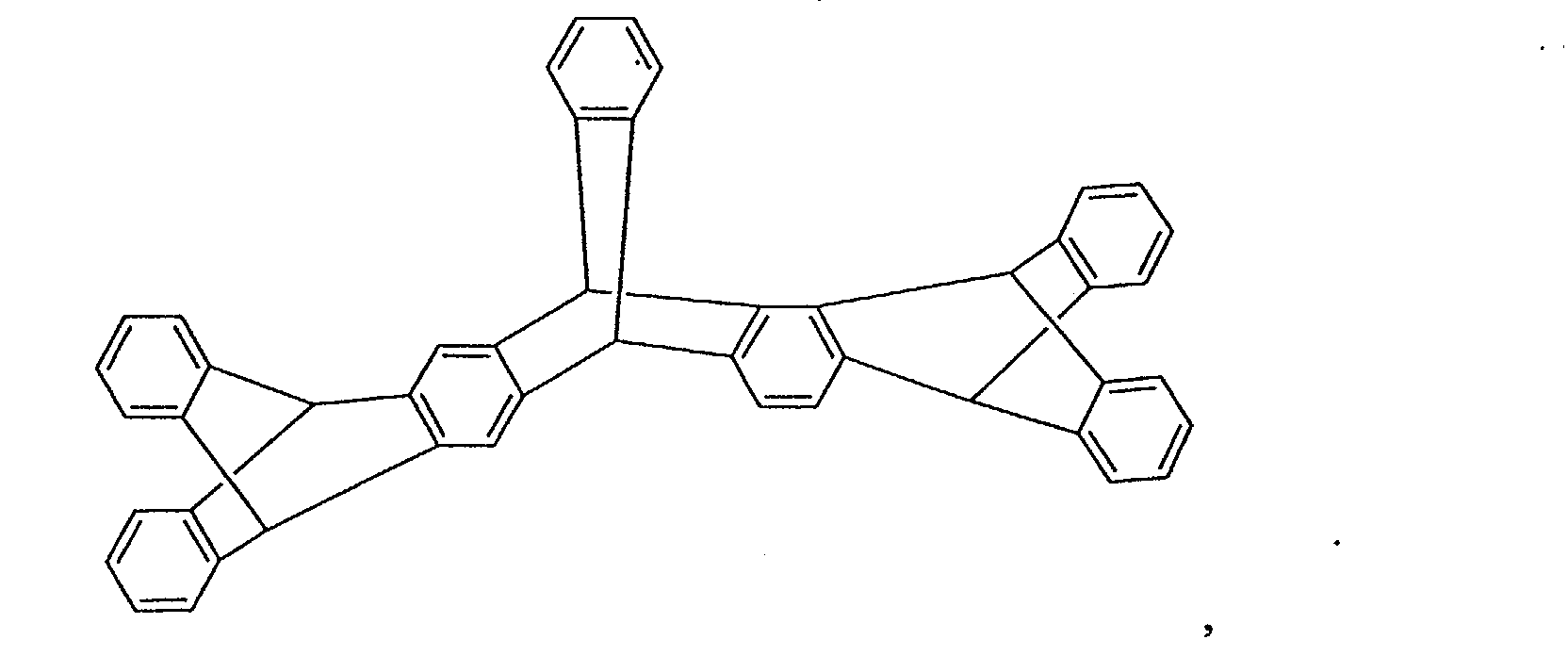
- the iptycene derivative is selected from the group consisting of and
- iptycenes have a rigid carbon framework, show exceptional thermal stability, and have well-defined 3-D molecular structures. Therefore, a device layer comprising small molecule iptycenes or small molecule iptycene derivatives, i.e., non-polymeric iptycenes, would prevent close molecular packing. As a result, high photoluminescent efficiency and possibly high electroluminescent efficiency can be achieved.
- Iptycene and iptycene derivatives suitable for use in the present invention can be produced according to any known method. Exemplary syntheses are disclosed in Shahlai, et al., "Synthesis of Three Helically Chiral Iptycenes", J. Org. Chem., vol. 56, no. 24, p. 6912 (1991); Shahlai, et al., “Synthesis of Supertriptycene and Two Related Iptycenes", J. Org. Chem., vol. 56, no. 24, p. 6905 (1991); Shahlai, et al.,"A Method for the Synthesis of Angular Iptycenes", J. Org. Chem., vol.
- triptycene is commercially available from a source such as Aldrich Chemical.
- the invention is an OLED in which an emissive layer is sandwiched between at least a cathode and an anode, and in which the emissive layer includes an iptycene derivative expressed according to the following general formula (I):
- R 1 -R 6 may be absent; wherein any or all of R 1 and R 2, R 3 and R 4, and R 5 and R 6 may be taken together to form an aryl group; and wherein any or all of R 1 -R 6 may represent a charge-transport substituent.
- R 1 -R 6 may be absent. If all of R 1 -R 6 are absent, then the iptycene derivative is unsubstituted triptycene.
- any or all of R 1 and R 2, R 3 and R 4, and R 5 and R 6 may be taken together to form an aryl group.
- R 1 and R 2 may be taken together to form an aryl group; alternatively or in addition, R 3 and R 4 may be taken together to form an aryl group; alternatively or in addition, R 5 and R 6 may be taken together to form an aryl group.
- the aryl group formed by any of these pairs is selected from the group consisting of and
- any or all of R 1 -R 6 may represent a charge-transport substituent.
- the presence of such a charge transport substituent can improve charge balance and enhance overall device performance.
- the charge transport substituent can be a hole transport group or an electron transport group.
- the charge transport substituent is selected from the group consisting of , and
- the iptycene derivative is selected from the group consisting of and
- the above-described iptycene derivative can be used directly as the emissive layer or can be used as a host material for an emissive dopant in a case where the emissive layer comprises an iptycene host plus an emissive dopant.
- Any known emissive material can be used as the emissive dopant.
- the amount of host or dopant in a given emissive layer varies depending on the overall desired result. Typically, the dopant is present in an amount of 0.1 - 20% by weight.
- a further aspect of the invention is directed to an OLED having an emissive layer sandwiched between at least one charge transport layer and an anode and a cathode.
- the charge transport layer can be either an electron transport layer or a hole transport layer, or both.
- the charge transport layer includes an iptycene derivative according to the above general formula (I) wherein R 1 through R 6 are specified above.
- the iptycene derivative is substituted with a charge transport group in order to enhance performance of the iptycene derivative as a charge transport material or host material therefor.
- the charge transport group can be a hole transport group or an electron transport group.
- the charge transport substituent is selected from hole transport groups such as
- the charge transport group is selected from electron transport groups such as and
- Iptycene derivatives substituted with hole transport groups suitable for use in the present invention include, without limitation:
- Iptycene derivatives substituted with electron transport groups suitable.for use in the present invention include, without limitation: and
- the compound expressed according to formula (I) can be used directly as the charge transport layer or can form a charge transport host material in a case where the charge transport layer comprises a host material plus a charge transport dopant.
- Any known charge transport material can be used as the emissive dopant.
- the amount of host or dopant in a given charge transport layer varies depending on the overall desired result.
- the dopant is present in an amount of 0.1 - 20% by weight.
- the deuterated 4-aldehydetriphenylamine was obtained by a reaction of triphenylamine (1 equiv.) and deuterated dimethylformamide-d7 (DMF-d7) (1.4 equiv.) in the presence of POCl 3 (1.2 equiv.) according to a similar reference procedure (see Li, et al., Chem. Mater., vol. 11, pp. 1568-1575(1999)).
- n-Butyllithium n-hexane solution (35.6 ml, 55 mmol) was added to a solution of 2-iododimethylfluorene (16 g, 50 mmol) dissolved in 170 ml of diethylether on a dry ice- acetone bath at -78 ° C under nitrogen. After stirring the slurry solution for 2.5 h, the reaction mixture was allowed to warm to room temperature, followed by stirring for 1 h. The solution was again cooled on the bath at -78°C. Trimethylborate (27.4 ml, 0.240 mmol) was then added to the solution. The solution was stirred at the low temperature for 1 h and at room temperature for 1 h.
- the water phase was extracted with toluene and ethyl acetate.
- the organic phase was dried over MgSO 4 and then the solvents were evaporated.
- the product was isolated by a silica gel column chromatography eluted by a 2:1 (or 3:1) mixture of n-hexane and toluene. If the product was not so pure, further purification using the silica gel column or recrystallization would be desirable. Pale yellow solid, Yield: 70%.
- An OLED was manufactured using compound 1 as an emissive material, NPD as a hole transporter, Bphen as an electron transporter, Li-Al alloy as an electron injection material and ITO and Al as electrode materials according to the method set forth below: 1,4-bis[(1-naphthyphenyl)-amino]biphenyl 4,7-diphenyl-1,10-phenanthroline (Bphen)
- a clean substrate coated with a patterned layer with an area of 0.0314 cm 2 of ITO was obtained.
- the substrate was treated with O 2 plasma for 1-5 minutes. Then, the substrate was placed in a thermal evaporator, and the pressure was pumped down below 6x10 -6 torr. Next, a 20 nm NPD hole transport layer was evaporated onto the substrate. Then, a 20 nm emissive layer consisting of Compound 1 was evaporated thereon. Then, a 40 nm Bphen electron transport layer was evaporated at a rate of approximately 1-3 ⁇ /s thereon. Next, a mask was placed next to the substrate to define where the metal is to be evaporated.
- the device obtained by the above process was tested for luminance, color, and current-voltage characteristics.
- a driving voltage was applied to the obtained device by connecting the ITO electrode to a positive electrode(+) and the Al cathode to a negative electrode(-) to test emission of light, and a uniform light of blue color was obtained.
- the following device data were obtained: the density of electric current: 300 mA/cm 2 at 8 V, the luminance: 1380 cd/m 2 at 8 V, and the maximum external quantum efficiency: 0.4 %, the maximum external power efficiency 0.45 lm/W, CIE color coordinates were (0.18, 0.15).
- An OLED was manufactured using compound 1 as host material for compound 5 as an emissive material, NPD as a hole transporter, Bphen as an electron transporter, Li-Al alloy as an electron injection material and ITO and Al as electrode materials according to the method set forth below:
- a clean substrate coated with a patterned layer with an area of 0.0314 cm 2 of ITO was obtained.
- the substrate was treated with O 2 plasma for 1-5 minutes. Then, the substrate was placed in a thermal evaporator, and the pressure was pumped down below 6x10 -6 torr. Next, a 20 nm NPD hole transport layer was evaporated onto the substrate. Then, a 30 nm emissive layer consisting of compound 1 and 1 % wt. compound 5 was formed thereon.
- evaporation of the dopant (compound 5) was stabilized at a rate around 0.03 ⁇ /s, then the evaporation of the host (compound 1) was stabilized at a rate around 1-3 ⁇ /s, giving a doping concentration of about 1-3%.
- the shutter was then opened, and the deposition was monitored by a quartz crystal monitor.
- a 30 nm Bphen electron transport layer was evaporated at a rate of approximately 1-3 ⁇ /s thereon.
- a mask was placed next to the substrate to define where the metal is to be evaporated.
- a 12 nm Li-Al (1:9) alloy was evaporated to improve electron injection into the device.
- a 150 nm A1 electrode was deposited, and the evaporator was allowed to cool.
- the driving voltage was applied to the obtained device by connecting the ITO electrode to a positive electrode(+) and the cathode of Al to a negative electrode(-) to test emission of light, and a uniform light of blue color was obtained.
- the following device data were obtained: the density of electric current: 30 mA/cm 2 at 8 V, the luminance: 600 cd/m 2 at 8 V, and the maximum external quantum efficiency: 1.4 %, the maximum external power efficiency 1.2 lm/W, CIE color coordinates were (0.15, 0.20).
- An OLED was manufactured using compound 1 as host material for compound 9 as a blue emissive material, NPD as a hole transporter, Bphen as an electron transporter, Li-Al alloy as an electron injection material and ITO and Al as electrode materials according to the method set forth below:
- a clean substrate coated with a patterned layer with an area of 0.0314 cm 2 of ITO was obtained.
- the substrate was treated with O 2 plasma for 1-5 minutes. Then, the substrate was placed in a thermal evaporator, and the pressure was pumped down below 6x 10 -6 torr. Next, a 20 nm NPD hole transport layer was evaporated onto the substrate. Then, a 30 nm emissive layer consisting of compound 1 and 1% wt. compound 9 was formed thereon.
- the driving voltage was applied to the obtained device by connecting the ITO electrode to a positive electrode(+) and the cathode of Al to a negative electrode(-) to test emission of light, and a uniform light of blue color was obtained.
- the following device data were obtained: the density of electric current: 40 mA/cm 2 at 8 V, the luminance: 400 cd/m 2 at 8 V, and the maximum external quantum efficiency: 1.2 %, the maximum external power efficiency 0.6 lm/W, CIE color coordinates were (0.17, 0.14).
- An OLED was manufactured using compound 1 as host material for compound 9 as a blue emissive material, NPD as a hole transporter, Bphen as an electron transporter, Li-Al alloy as an electron injection material and ITO and Al as electrode materials according to the method set forth below:
- a clean substrate coated with a patterned layer with an area of 0.0314 cm 2 of ITO was obtained.
- the substrate was treated with O 2 plasma for 1-5 minutes. Then, the substrate was placed in a thermal evaporator, and the pressure was pumped down below 6x10 -6 torr. Next, a 20 nm NPD hole transport layer was evaporated onto the substrate. Then, a 30 nm emissive layer consisting of compound 1 and 2% wt. compound 9 was formed thereon.
- the driving voltage was applied to the obtained device by connecting the ITO electrode to a positive electrode(+) and the cathode of A1 to a negative electrode(-) to test emission of light, and a uniform light of blue color was obtained.
- the following device data were obtained: the density of electric current: 60 mA/cm 2 at 6 V, the luminance: 750 cd/m 2 at 6 V, and the maximum external quantum efficiency: 1.7 %, the maximum external power efficiency 1.4 lm/W, CIE color coordinates were (0.16, 0.13).
- An OLED was manufactured using compound 2 as host material for compound 9 as a blue emissive material, NPD as a hole transporter, Bphen as an electron transporter, Li-Al alloy as an electron injection material and ITO and Al as electrode materials according to the method set forth below:
- a clean substrate coated with a patterned layer with an area of 0.0314 cm 2 of ITO was obtained.
- the substrate was treated with O 2 plasma for 1-5 minutes. Then, the substrate was placed in a thermal evaporator, and the pressure was pumped down below 6x10 -6 torr. Next, a 20 nm NPD hole transport layer was evaporated onto the substrate. Then, a 30 nm emissive layer consisting of compound 2 and 2% wt. compound 9 was formed thereon.
- the driving voltage was applied to the obtained device by connecting the ITO electrode to a positive electrode(+) and the cathode of Al to a negative electrode(-) to test emission of light, and a uniform light of blue color was obtained.
- the following device data were obtained: the density of electric current: 40 mA/cm 2 at 6 V, the luminance: 300 cd/m 2 at 6 V, and the maximum external quantum efficiency: 1.2 %, the maximum external power efficiency 0.9 lm/W, CIE color coordinates were (0.18, 0.15).
Abstract
Description
- The present invention relates to an organic light emitting device (OLED) in which small molecule iptycene derivatives are used as the emissive layer and/or one or more of the charge transport layers, or as a host material for one or more of such layers.
- Significant efforts have been expended in developing suitable materials for use in organic light emitting devices (OLEDs). Such devices are commercially attractive because they offer the promise of low-cost fabrication of high-density pixeled displays exhibiting bright electroluminescence with long life times and wide color range.
- A typical OLED is fabricated by sandwiching an emissive layer between an anode and a cathode. When a bias is applied across the electrodes, holes and electrons are respectively injected from the anode and cathode into the emissive layer, typically facilitated by hole transport and electron transport layers (charge transport layers) adjacent to the respective electrodes. The holes and electrons radiatively combine in the emissive layer and emit light. Improved performance can be obtained if blocking layers are provided to block against the injection of either holes or electrons from the adjoining layer and their subsequent escape from the device. Some of these layers can be combined. For example, a double-layered structure is fabricated from a combined hole-injecting and transporting layer together with a combined electron-transporting and light-emitting layer. Likewise, a triple-layered structure is composed of a hole-injecting and transporting layer, a light-emitting layer, and an electron-injecting and transporting layer.
- In addition, it is possible to form these layers from a host material doped with another material designed to achieve the desired effect of the layer (for example, to achieve a hole transport effect, an electron transport effect, or an emissive effect).
- Because of consumer expectations of good efficiency, long lifetime and pure color, a need exists for development of suitable materials for the various layers.
- It is an object of the invention to provide an improved OLED in which iptycene derivatives are used as the emissive layer and/or one or more of the charge transport layers, or as a host material for one or more of such layers.
- Thus, in one aspect, the invention is an OLED in which an emissive layer is sandwiched between at least a cathode and an anode, and in which the emissive layer includes an iptycene derivative expressed according to the following general formula (I):

- wherein any or all of R1-R6 may be absent; wherein any or all of R1 and R2, R3 and R4, and R5 and R6 may be taken together to form an aryl group; and wherein any or all of R1-R6 may represent a charge-transport substituent.
- The compound expressed according to formula (I) can be used directly as the emissive layer, or can be used as a host material for an emissive dopant in a case where the emissive layer comprises an iptycene host plus an emissive dopant.
- In a further aspect, the invention is an OLED having an emissive layer sandwiched between at least one charge transport layer and an anode and a cathode. The charge transport layer can be either an electron transport layer or a hole transport layer, or both. According to this aspect of the invention, the charge transport layer includes an iptycene derivative according to the above general formula (I) wherein R, through R6 are specified above.
- According to this aspect, the compound expressed according to formula (I) can be used directly as the charge transport layer or can form a charge transport host material in a case where the charge transport layer comprises a host material plus a charge transport dopant.
- In certain preferred embodiments of the present invention, any or all of R1 and R2, R3 and R4, and R5 and R6 are taken together to form an aryl group selected from the group consisting of


- In certain preferred embodiments of the present invention, any or all of R1-R6 represents a charge-transport substituent selected from the group consisting of


- In preferred embodiments of the present invention, the iptycene derivative is selected from the group consisting of


- This brief summary has been provided so that the nature of the invention may be understood quickly. A more complete understanding of the invention can be obtained by reference to the following detailed description of the preferred embodiment thereof in connection with the attached drawings.
- In general, iptycenes have a rigid carbon framework, show exceptional thermal stability, and have well-defined 3-D molecular structures. Therefore, a device layer comprising small molecule iptycenes or small molecule iptycene derivatives, i.e., non-polymeric iptycenes, would prevent close molecular packing. As a result, high photoluminescent efficiency and possibly high electroluminescent efficiency can be achieved.
- Iptycene and iptycene derivatives suitable for use in the present invention can be produced according to any known method. Exemplary syntheses are disclosed in Shahlai, et al., "Synthesis of Three Helically Chiral Iptycenes", J. Org. Chem., vol. 56, no. 24, p. 6912 (1991); Shahlai, et al., "Synthesis of Supertriptycene and Two Related Iptycenes", J. Org. Chem., vol. 56, no. 24, p. 6905 (1991); Shahlai, et al.,"A Method for the Synthesis of Angular Iptycenes", J. Org. Chem., vol. 54, no. 11, pp. 2615 (1989); and Hart, et al., "Iptycenes: Extended Triptycenes", Tetrahedron, vol. 42, no. 6, pp. 1641 (1986). In addition, unsubstituted triptycene is commercially available from a source such as Aldrich Chemical.
- Accordingly, in one aspect the invention is an OLED in which an emissive layer is sandwiched between at least a cathode and an anode, and in which the emissive layer includes an iptycene derivative expressed according to the following general formula (I):

- wherein any or all of R1-R6 may be absent; wherein any or all of R1 and R2, R3 and R4, and R5 and R6 may be taken together to form an aryl group; and wherein any or all of R1-R6 may represent a charge-transport substituent.
- Any or all of R1-R6 may be absent. If all of R1-R6 are absent, then the iptycene derivative is unsubstituted triptycene.
- When present, any or all of R1 and R2, R3 and R4, and R5 and R6 may be taken together to form an aryl group. For example, R1 and R2 may be taken together to form an aryl group; alternatively or in addition, R3 and R4 may be taken together to form an aryl group; alternatively or in addition, R5 and R6 may be taken together to form an aryl group. In certain preferred embodiments of the present invention, the aryl group formed by any of these pairs is selected from the group consisting of


- Further, when present, any or all of R1-R6 may represent a charge-transport substituent. The presence of such a charge transport substituent can improve charge balance and enhance overall device performance. The charge transport substituent can be a hole transport group or an electron transport group. In preferred embodiments of the present invention, the charge transport substituent is selected from the group consisting of


- In preferred embodiments of the present invention, the iptycene derivative is selected from the group consisting of


- In this aspect of the invention, the above-described iptycene derivative can be used directly as the emissive layer or can be used as a host material for an emissive dopant in a case where the emissive layer comprises an iptycene host plus an emissive dopant. Any known emissive material can be used as the emissive dopant. One ordinarily skilled in the art would readily understand that the amount of host or dopant in a given emissive layer varies depending on the overall desired result. Typically, the dopant is present in an amount of 0.1 - 20% by weight.
- A further aspect of the invention is directed to an OLED having an emissive layer sandwiched between at least one charge transport layer and an anode and a cathode. The charge transport layer can be either an electron transport layer or a hole transport layer, or both. According to this aspect of the invention, the charge transport layer includes an iptycene derivative according to the above general formula (I) wherein R1 through R6 are specified above.
- In a preferred embodiment of this aspect of the invention, the iptycene derivative is substituted with a charge transport group in order to enhance performance of the iptycene derivative as a charge transport material or host material therefor. The charge transport group can be a hole transport group or an electron transport group. In preferred embodiments of the present invention, the charge transport substituent is selected from hole transport groups such as


- In other preferred embodiments, the charge transport group is selected from electron transport groups such as


- Iptycene derivatives substituted with hole transport groups suitable for use in the present invention include, without limitation:


- Iptycene derivatives substituted with electron transport groups suitable.for use in the present invention include, without limitation:


- According to this aspect of the invention, the compound expressed according to formula (I) can be used directly as the charge transport layer or can form a charge transport host material in a case where the charge transport layer comprises a host material plus a charge transport dopant. Any known charge transport material can be used as the emissive dopant. One ordinarily skilled in the art would readily understand that the amount of host or dopant in a given charge transport layer varies depending on the overall desired result. Typically, the dopant is present in an amount of 0.1 - 20% by weight.
- The following specific examples of the synthesis of iptycene derivatives and of OLEDs incorporating such iptycene derivatives in accordance with the present invention are for illustration purposes and are not to be considered limiting of the invention, which is defined by the claims.
- Synthesis of Compounds 1, 2, 3


- Compounds 1, 2, and 3 (dibromotriptycene) were synthesized according to known procedures (see Hart, et al., "Iptycenes: Extended Triptycenes", Tetrahedron, vol. 42, no. 6, p. 1641 (1986)).
- Synthesis of Compound 4

- A round flask was charged with compound 3 (0.824 g, 2 mmol), 4-biphenylboronic acid (1.2 g, 6 mmol), Pd(0)(PPh3)4 (120 mg), and a mixture of 20 mL of dry toluene and 10 mL of dry ethanol. After stirring for 10 min at room temperature, a 10 mL solution of degassed 2M of aqueous Na2CO3 was added to the reaction solution. The reaction mixtures were stirred at 80 °C under N2 for two days. After cooling down, the mixture was poured into water. The product was extracted with toluene, washed with water, dried over MgSO4. After filtration and concentration, it was purified through column chromatography (silica gel, mixtures of CH2Cl2/hexanes). Yield: 75%. It had a Td at 310°C by TGA.
-

- Compound 5 was synthesized via a few step reactions. 2,2'-dibromomethyl-1,1'-binaphthyl was obtained by reaction of N-bromosuccinimide (NBS) with 2,2'-dimethyl-1,1'-binaphthyl according to a known reference procedure (see Maigrot et al., Synthesis, pp. 317-320 (1985)). Refluxing of 2,2'-dibromomcthyl-1,1 '-binaphthyl in an excess of triethylphosphite afforded the ester compound. The deuterated 4-aldehydetriphenylamine was obtained by a reaction of triphenylamine (1 equiv.) and deuterated dimethylformamide-d7 (DMF-d7) (1.4 equiv.) in the presence of POCl3 (1.2 equiv.) according to a similar reference procedure (see Li, et al., Chem. Mater., vol. 11, pp. 1568-1575(1999)). Finally, a round flask was charged with 1,1'-binaphthyl ester compound (0.77 g, 1.39 mmol), deuterated 4-aldehydetriphenylamine (0.8 g, 2.92 mmol), NaOt-Bu (0.4 g, 4.17 mmol), and 10 mL of dry DMF. The mixture was stirred at room temperature under N2 for two days. The mixture was poured into 100 mL of water. The precipitate was filtered and washed with water and methanol. It was purified through column chromatography (silica gel, mixtures of CH2Cl2/hexanes). Yield: 50%. It had a Tg at 122 °C by DSC. This compound shows a good blue emission.
-

- 15% n-Butyllithium n-hexane solution (35.6 ml, 55 mmol) was added to a solution of 2-iododimethylfluorene (16 g, 50 mmol) dissolved in 170 ml of diethylether on a dry ice- acetone bath at -78 ° C under nitrogen. After stirring the slurry solution for 2.5 h, the reaction mixture was allowed to warm to room temperature, followed by stirring for 1 h. The solution was again cooled on the bath at -78°C. Trimethylborate (27.4 ml, 0.240 mmol) was then added to the solution. The solution was stirred at the low temperature for 1 h and at room temperature for 1 h. The resulting reaction mixture was stand alone at room temperature over night. Half of the solvent was evaporated, followed by adding 50 ml of water and continuously 140 ml of 2M HC1 aqueous solution. The precipitate was filtrated and washed with toluene. The solvent was removed from the organic phase, giving the additional boronic acid. The solid was also washed with toluene.
The product was dried in vacuo. White solid, Yield: 70%. -

- 2-Iododimethylfluorene (1.98 g, 6.18 mmol) and 1.5 g (4.73 mmol) of dimethylfluorene-2-boronic acid were dissolved in a mixture of degassed toluene (80 ml) and degassed ethanol (40 ml). Sodium carbonate aqueous solution (41 ml), which was prepared by dissolving 9 g of sodium carbonate in 45 ml of water, was added to the solution, followed by stirring at room temperature for 30 min. To the resulting hazy solution was added 238 mg (0.206 mmol) of Pd(PPh3)4 as a solid. The solution was then heated on an oil bath at 80 °C for 5 h under nitrogen flow.
After cooling to room temperature, ethyl acetate and water were added to the reaction mixture. The organic phase and the water phase were separated. The water phase was extracted with toluene and ethyl acetate. The combined organic phase was dried over MgSO4 and the solvents were evaporated. The desirable product was isolated by a silica-gel column chromatography eluted by a 2:1 (or 3:1) mixture of n-hexane and toluene. If the product was not so pure, further purification using the silica-gel column would be desirable. White pale yellow solid, Yield: 90%. -

- To compound 7 (350 mg, 0.907 mmol), 164 mg (0.72 mmol) of H5I6O6-H2O, and 366 mg of I2 (2.88 mmol) in 20 ml of acetic acid was added a mixture of H2SO4 (6 ml) and H2O (4 ml). The solution was stirred at 80°C for 3 h, giving a pale red solution. After cooling the solution to room temperature, water was added. The solid thus precipitated was filtrated, followed by washing the precipitate with water and n-hexane. The product was dried in vacuo. Pale red solid (when purified by a silica gel column, the pale red color disappeared), Yield: 80%.
-

- To a solution of Pd(dba)2 (72 mg, 0.125 mmol) in 10 ml of toluene was added 76 mg of tris(tert-butyl)phosphine in 3 ml of toluene, followed by stirring for 30 min under nitrogen. 2,7-Diiododimethylfluorene (360 mg, 0.564 mmol) dissolved in 20 ml of toluene was added to the dark-brown catalyst solution. After stirring the solution for about 20min, 217 mg (2.26 mmol) of sodium tert-butoxide was added as a solid. The solution was heated on an oil-bath at 80°C for 5 h. The reaction mixture was quenched with water. The water phase was extracted with toluene and ethyl acetate. The organic phase was dried over MgSO4 and then the solvents were evaporated. The product was isolated by a silica gel column chromatography eluted by a 2:1 (or 3:1) mixture of n-hexane and toluene. If the product was not so pure, further purification using the silica gel column or recrystallization would be desirable. Pale yellow solid, Yield: 70%.
- An OLED was manufactured using compound 1 as an emissive material, NPD as a hole transporter, Bphen as an electron transporter, Li-Al alloy as an electron injection material and ITO and Al as electrode materials according to the method set forth below:


- A clean substrate coated with a patterned layer with an area of 0.0314 cm2 of ITO was obtained. The substrate was treated with O2 plasma for 1-5 minutes. Then, the substrate was placed in a thermal evaporator, and the pressure was pumped down below 6x10⁻⁶ torr. Next, a 20 nm NPD hole transport layer was evaporated onto the substrate. Then, a 20 nm emissive layer consisting of Compound 1 was evaporated thereon. Then, a 40 nm Bphen electron transport layer was evaporated at a rate of approximately 1-3 Å/s thereon. Next, a mask was placed next to the substrate to define where the metal is to be evaporated. Then, a 12 nm Li-Al (1:9) alloy was evaporated to improve electron injection into the device. Finally, a 150 nm Al electrode was deposited, and the evaporator was allowed to cool. Evaporation was accomplished using an ULVAC VPC-1100 (Sinku Kiko).
- The device obtained by the above process was tested for luminance, color, and current-voltage characteristics. A driving voltage was applied to the obtained device by connecting the ITO electrode to a positive electrode(+) and the Al cathode to a negative electrode(-) to test emission of light, and a uniform light of blue color was obtained. The following device data were obtained: the density of electric current: 300 mA/cm2 at 8 V, the luminance: 1380 cd/m2 at 8 V, and the maximum external quantum efficiency: 0.4 %, the maximum external power efficiency 0.45 lm/W, CIE color coordinates were (0.18, 0.15).
- An OLED was manufactured using compound 1 as host material for compound 5 as an emissive material, NPD as a hole transporter, Bphen as an electron transporter, Li-Al alloy as an electron injection material and ITO and Al as electrode materials according to the method set forth below:
- A clean substrate coated with a patterned layer with an area of 0.0314 cm2 of ITO was obtained. The substrate was treated with O2 plasma for 1-5 minutes. Then, the substrate was placed in a thermal evaporator, and the pressure was pumped down below 6x10⁻⁶ torr. Next, a 20 nm NPD hole transport layer was evaporated onto the substrate. Then, a 30 nm emissive layer consisting of compound 1 and 1 % wt. compound 5 was formed thereon. With the shutter of the deposition chamber closed to prevent premature deposition, evaporation of the dopant (compound 5) was stabilized at a rate around 0.03 Å/s, then the evaporation of the host (compound 1) was stabilized at a rate around 1-3 Å/s, giving a doping concentration of about 1-3%. The shutter was then opened, and the deposition was monitored by a quartz crystal monitor. Then, a 30 nm Bphen electron transport layer was evaporated at a rate of approximately 1-3 Å/s thereon. Next, a mask was placed next to the substrate to define where the metal is to be evaporated. Then, a 12 nm Li-Al (1:9) alloy was evaporated to improve electron injection into the device. Finally, a 150 nm A1 electrode was deposited, and the evaporator was allowed to cool.
- The driving voltage was applied to the obtained device by connecting the ITO electrode to a positive electrode(+) and the cathode of Al to a negative electrode(-) to test emission of light, and a uniform light of blue color was obtained. The following device data were obtained: the density of electric current: 30 mA/cm2 at 8 V, the luminance: 600 cd/m2 at 8 V, and the maximum external quantum efficiency: 1.4 %, the maximum external power efficiency 1.2 lm/W, CIE color coordinates were (0.15, 0.20).
- An OLED was manufactured using compound 1 as host material for compound 9 as a blue emissive material, NPD as a hole transporter, Bphen as an electron transporter, Li-Al alloy as an electron injection material and ITO and Al as electrode materials according to the method set forth below:
- A clean substrate coated with a patterned layer with an area of 0.0314 cm2 of ITO was obtained. The substrate was treated with O2 plasma for 1-5 minutes. Then, the substrate was placed in a thermal evaporator, and the pressure was pumped down below 6x 10⁻⁶ torr. Next, a 20 nm NPD hole transport layer was evaporated onto the substrate. Then, a 30 nm emissive layer consisting of compound 1 and 1% wt. compound 9 was formed thereon. With the shutter of the deposition chamber closed to prevent premature deposition, evaporation of the dopant (compound 9) was stabilized at a rate around 0.03 Å/s, then the evaporation of the host (compound 1) was stabilized at a rate around 1-3 Å/s, giving a doping concentration of about 1-3%. The shutter was then opened, and the deposition was monitored by a quartz crystal monitor. Then, a 30 nm Bphen electron transport layer was evaporated at a rate of approximately 1-3 Å/s thereon. Next, a mask was placed next to the substrate to define where the metal is to be evaporated. Then, a 12 nm Li-Al (1:9) alloy was evaporated to improve electron injection into the device. Finally, a 150 nm Al electrode was deposited, and the evaporator was allowed to cool.
- The driving voltage was applied to the obtained device by connecting the ITO electrode to a positive electrode(+) and the cathode of Al to a negative electrode(-) to test emission of light, and a uniform light of blue color was obtained. The following device data were obtained: the density of electric current: 40 mA/cm2 at 8 V, the luminance: 400 cd/m2 at 8 V, and the maximum external quantum efficiency: 1.2 %, the maximum external power efficiency 0.6 lm/W, CIE color coordinates were (0.17, 0.14).
- An OLED was manufactured using compound 1 as host material for compound 9 as a blue emissive material, NPD as a hole transporter, Bphen as an electron transporter, Li-Al alloy as an electron injection material and ITO and Al as electrode materials according to the method set forth below:
- A clean substrate coated with a patterned layer with an area of 0.0314 cm2 of ITO was obtained. The substrate was treated with O2 plasma for 1-5 minutes. Then, the substrate was placed in a thermal evaporator, and the pressure was pumped down below 6x10⁻⁶ torr. Next, a 20 nm NPD hole transport layer was evaporated onto the substrate. Then, a 30 nm emissive layer consisting of compound 1 and 2% wt. compound 9 was formed thereon. With the shutter of the deposition chamber closed to prevent premature deposition, evaporation of the dopant (compound 9) was stabilized at a rate around 0.03 Å/s, then the evaporation of the host (compound 1) was stabilized at a rate around 1-3 Å/s, giving a doping concentration of about 1-3%. The shutter was then opened, and the deposition was monitored by a quartz crystal monitor. Then, a 30 nm Bphen electron transport layer was evaporated at a rate of approximately 1-3 Å/s thereon. Next, a mask was placed next to the substrate to define where the metal is to be evaporated. Then, a 12 nm Li-Al (1:9) alloy was evaporated to improve electron injection into the device. Finally, a 150 nm Al electrode was deposited, and the evaporator was allowed to cool.
- The driving voltage was applied to the obtained device by connecting the ITO electrode to a positive electrode(+) and the cathode of A1 to a negative electrode(-) to test emission of light, and a uniform light of blue color was obtained. The following device data were obtained: the density of electric current: 60 mA/cm2 at 6 V, the luminance: 750 cd/m2 at 6 V, and the maximum external quantum efficiency: 1.7 %, the maximum external power efficiency 1.4 lm/W, CIE color coordinates were (0.16, 0.13).
- An OLED was manufactured using compound 2 as host material for compound 9 as a blue emissive material, NPD as a hole transporter, Bphen as an electron transporter, Li-Al alloy as an electron injection material and ITO and Al as electrode materials according to the method set forth below:
- A clean substrate coated with a patterned layer with an area of 0.0314 cm2 of ITO was obtained. The substrate was treated with O2 plasma for 1-5 minutes. Then, the substrate was placed in a thermal evaporator, and the pressure was pumped down below 6x10⁻⁶ torr. Next, a 20 nm NPD hole transport layer was evaporated onto the substrate. Then, a 30 nm emissive layer consisting of compound 2 and 2% wt. compound 9 was formed thereon. With the shutter of the deposition chamber closed to prevent premature deposition, evaporation of the dopant (compound 9) was stabilized at a rate around 0.03 Å/s, then the evaporation of the host (compound 1) was stabilized at a rate around 1-3 Å/s, giving a doping concentration of about 1-3%. The shutter was then opened, and the deposition was monitored by a quartz crystal monitor. Then, a 30 nm Bphen electron transport layer was evaporated at a rate of approximately 1-3 Å/s thereon. Next, a mask was placed next to the substrate to define where the metal is to be evaporated. Then, a 12 nm Li-Al (1:9) alloy was evaporated to improve electron injection into the device. Finally, a 150 nm Al electrode was deposited, and the evaporator was allowed to cool.
- The driving voltage was applied to the obtained device by connecting the ITO electrode to a positive electrode(+) and the cathode of Al to a negative electrode(-) to test emission of light, and a uniform light of blue color was obtained. The following device data were obtained: the density of electric current: 40 mA/cm2 at 6 V, the luminance: 300 cd/m2 at 6 V, and the maximum external quantum efficiency: 1.2 %, the maximum external power efficiency 0.9 lm/W, CIE color coordinates were (0.18, 0.15).
- The preceding examples are provided to illustrate the invention, and are not to be considered limiting of the invention, which is defined by the following claims.
Claims (15)
- An organic light emitting device comprising:an emissive layer sandwiched between at least a cathode and an anode, wherein the emissive layer includes an iptycene derivative expressed according to the following general formula (I):wherein any or all of R1-R6 may be absent;

wherein any or all of R1 and R2, R3 and R4, and R5 and R6 may be taken together to form an aryl group; and
wherein any or all of R1-R6 may represent a charge-transport substituent. - The organic light emitting device according to Claim 1, wherein any or all of R1 and R2, R3 and R4, and R5 and R6 are taken together to form an aryl group selected from the group consisting of


- The organic light emitting device according to Claim 1, wherein any or all of R1-R6 represents a charge-transport substituent selected from the group consisting of


- The organic light emitting device according to Claim 1, wherein the iptycene derivative is selected from the group consisting of


- The organic light emitting device according to Claim 1, wherein said emissive layer is comprised of a functional light-emitting layer of the iptycene derivative.
- The organic light emitting device according to Claim 1, wherein said emissive layer is comprised of a host material of the iptycene derivative, together with a functional light-emitting dopant.
- An organic light emitting device comprising:an emissive layer sandwiched between at least one charge transport layer and an anode and a cathode, wherein the charge transport layer includes an iptycene derivative according to the following general formula (I):wherein any or all of R1-R6 may be absent;

wherein any or all of R, and R2, R3 and R4, and R5 and R6 may be taken together to form an aryl group; and
wherein any or all of R1-R6 may represent a charge-transport substituent. - The organic light emitting device according to Claim 7, wherein any or all of R1 and R2, R3 and R4, and R5 and R6 are taken together to form an aryl group selected from the group consisting of


- The organic light emitting device according to Claim 7, wherein any or all of R1-R6 represents a charge-transport substituent selected from the group consisting of


- The organic light emitting device according to Claim 7,
wherein the iptycene derivative is selected from the group consisting of


- The organic light emitting device according to Claim 7, wherein said charge transport layer is comprised of a functional charge transport layer of the iptycene derivative.
- The organic light emitting device according to Claim 7, wherein said charge transport layer is comprised of a host material of the iptycene derivative, together with a functional charge transport dopant.
- The organic light emitting device according to Claim 7, wherein the charge transport layer is an electron transport layer.
- The organic light emitting device according to Claim 7, wherein the charge transport layer is a hole transport layer.
- An organic light emitting device comprising:an emissive layer sandwiched between at least a cathode and an anode, andoptionally at least one charge transport layer;wherein the emissive layer and or the or a charge transport layer includes an iptycene derivative expressed according to the following general formula (I):

wherein any or all of R1 and R2, R3 and R4, and R5 and R6 may be taken together to form an aryl group; and
wherein any or all of R1-R6 may represent a charge-transport substituent.
Applications Claiming Priority (2)
| Application Number | Priority Date | Filing Date | Title |
|---|---|---|---|
| US230273 | 2002-08-29 | ||
| US10/230,273 US20040048099A1 (en) | 2002-08-29 | 2002-08-29 | Organic light-emitting device using iptycene derivatives |
Publications (1)
| Publication Number | Publication Date |
|---|---|
| EP1413617A1 true EP1413617A1 (en) | 2004-04-28 |
Family
ID=31990382
Family Applications (1)
| Application Number | Title | Priority Date | Filing Date |
|---|---|---|---|
| EP03255112A Withdrawn EP1413617A1 (en) | 2002-08-29 | 2003-08-18 | Organic light-emitting device using iptycene derivatives |
Country Status (4)
| Country | Link |
|---|---|
| US (2) | US20040048099A1 (en) |
| EP (1) | EP1413617A1 (en) |
| JP (1) | JP3762398B2 (en) |
| CN (1) | CN1479561A (en) |
Families Citing this family (18)
| Publication number | Priority date | Publication date | Assignee | Title |
|---|---|---|---|---|
| US5869079A (en) * | 1995-06-02 | 1999-02-09 | Oculex Pharmaceuticals, Inc. | Formulation for controlled release of drugs by combining hydrophilic and hydrophobic agents |
| WO2003023876A1 (en) * | 2001-09-05 | 2003-03-20 | Sharp Kabushiki Kaisha | Polymer structure and functional element having the same, and transistor and display using the same |
| WO2006016684A1 (en) * | 2004-08-11 | 2006-02-16 | Semiconductor Energy Laboratory Co., Ltd. | Method for synthesis of aromatic amine |
| JP4939780B2 (en) * | 2004-08-11 | 2012-05-30 | 株式会社半導体エネルギー研究所 | Method for synthesizing aromatic amines |
| WO2008121124A1 (en) | 2007-03-19 | 2008-10-09 | Nomadics, Inc. | Hydrogen peroxide detector and methods |
| DE102008007551A1 (en) | 2008-02-05 | 2009-08-06 | Bayer Materialscience Ag | Organometallic framework compounds based on triptycene |
| KR100901887B1 (en) * | 2008-03-14 | 2009-06-09 | (주)그라쎌 | Novel organic electroluminescent compounds and organic electroluminescent device using the same |
| TWI458694B (en) * | 2009-01-19 | 2014-11-01 | Nippon Steel & Sumikin Chem Co | Organic light field components |
| KR20120086319A (en) * | 2009-10-19 | 2012-08-02 | 이 아이 듀폰 디 네모아 앤드 캄파니 | Triarylamine compounds for electronic applications |
| CN103420897B (en) * | 2013-01-09 | 2015-11-25 | 烟台九目化学制品有限公司 | A kind of Triptycene derivative and application thereof |
| US11239432B2 (en) * | 2016-10-14 | 2022-02-01 | Universal Display Corporation | Organic electroluminescent materials and devices |
| JP7318178B2 (en) * | 2017-03-21 | 2023-08-01 | 東ソー株式会社 | Cyclic azine compounds, materials for organic electroluminescence devices, electron transport materials for organic electroluminescence devices |
| WO2018173882A1 (en) * | 2017-03-21 | 2018-09-27 | 東ソー株式会社 | Cyclic azine compound, material for organic electroluminescent element, and electron transport material for organic electroluminescent element |
| WO2019163959A1 (en) * | 2018-02-26 | 2019-08-29 | 東ソー株式会社 | Cyclic azine compound, material for organic electroluminescnet element, and electron-transporting material for organic electroluminescent element |
| JP7379830B2 (en) * | 2018-02-26 | 2023-11-15 | 東ソー株式会社 | Cyclic azine compounds, materials for organic electroluminescent devices, and electron transport materials for organic electroluminescent devices |
| KR20200072891A (en) * | 2018-12-13 | 2020-06-23 | 엘지디스플레이 주식회사 | Delayed fluorescence compound, and Organic light emitting diode and Organic light emitting display device including the same |
| CN111995562A (en) * | 2020-09-14 | 2020-11-27 | 深圳大学 | Triptycene D-A type thermal activation delayed fluorescent material, electronic device and application |
| CN113912646A (en) * | 2021-11-18 | 2022-01-11 | 浙江新化化工股份有限公司 | Preparation method of bidentate phosphine ligand |
Citations (2)
| Publication number | Priority date | Publication date | Assignee | Title |
|---|---|---|---|---|
| WO2002016463A2 (en) * | 2000-08-21 | 2002-02-28 | Massachusetts Institute Of Technology | Polymers with high internal free volume |
| EP1281744A2 (en) * | 1998-05-05 | 2003-02-05 | Massachusetts Institute Of Technology | Emissive polymers and devices incorporating these polymers |
Family Cites Families (18)
| Publication number | Priority date | Publication date | Assignee | Title |
|---|---|---|---|---|
| US4363746A (en) * | 1979-05-29 | 1982-12-14 | Phillips Petroleum Company | Composition of matter and method of preparing same, catalyst, method of producing the catalyst and polymerization process employing the catalyst |
| US4371690A (en) * | 1979-07-12 | 1983-02-01 | E. I. Du Pont De Nemours And Company | Heat-resistant rigid polymers from difunctional 9,10-dihydro-9,10-ethanoanthracenes |
| US4435548A (en) * | 1981-04-27 | 1984-03-06 | The Dow Chemical Company | Branched polyamidoamines |
| US4631337A (en) * | 1983-01-07 | 1986-12-23 | The Dow Chemical Company | Hydrolytically-stable dense star polyamine |
| US4558120A (en) * | 1983-01-07 | 1985-12-10 | The Dow Chemical Company | Dense star polymer |
| US4507466A (en) * | 1983-01-07 | 1985-03-26 | The Dow Chemical Corporation | Dense star polymers having core, core branches, terminal groups |
| US4626361A (en) * | 1983-03-09 | 1986-12-02 | Eastman Kodak Company | Binder-mixtures for optical recording layers and elements |
| US4883898A (en) * | 1987-12-10 | 1989-11-28 | University Of Chicago | Chemiluminescent compounds |
| US4946890A (en) * | 1988-08-11 | 1990-08-07 | The United States Of America As Represented By The Administrator, National Aeronautics And Space Administration | Novel ladder polymers for use as high temperature stable resins or coatings |
| US5041516A (en) * | 1989-06-21 | 1991-08-20 | Cornell Research Foundation, Inc. | Dendritic molecules and method of production |
| US6025462A (en) * | 1997-03-06 | 2000-02-15 | Eic Laboratories, Inc. | Reflective and conductive star polymers |
| DE19744792A1 (en) * | 1997-10-10 | 1999-04-15 | Hoechst Ag | Triptycene derivatives for use in electroluminescent devices |
| ATE409215T1 (en) * | 1998-05-05 | 2008-10-15 | Massachusetts Inst Technology | EMITTING POLYMERS AND DEVICES CONTAINING THESE POLYMERS |
| US6361886B2 (en) * | 1998-12-09 | 2002-03-26 | Eastman Kodak Company | Electroluminescent device with improved hole transport layer |
| EP1011154B1 (en) * | 1998-12-15 | 2010-04-21 | Sony Deutschland GmbH | Polyimide layer comprising functional material, device employing the same and method of manufacturing same device |
| US6294245B1 (en) * | 1999-09-22 | 2001-09-25 | Agilent Technologies, Inc. | Method for depositing electrically conducting polymer films via electrochemical deposition of precursor polymers |
| US6268072B1 (en) * | 1999-10-01 | 2001-07-31 | Eastman Kodak Company | Electroluminescent devices having phenylanthracene-based polymers |
| US7186355B2 (en) * | 2000-02-04 | 2007-03-06 | Massachusetts Institute Of Technology | Insulated nanoscopic pathways, compositions and devices of the same |
-
2002
- 2002-08-29 US US10/230,273 patent/US20040048099A1/en not_active Abandoned
-
2003
- 2003-07-04 CN CNA031462502A patent/CN1479561A/en active Pending
- 2003-08-18 EP EP03255112A patent/EP1413617A1/en not_active Withdrawn
- 2003-08-27 JP JP2003303405A patent/JP3762398B2/en not_active Expired - Fee Related
-
2004
- 2004-07-06 US US10/883,802 patent/US6962758B2/en not_active Expired - Fee Related
Patent Citations (2)
| Publication number | Priority date | Publication date | Assignee | Title |
|---|---|---|---|---|
| EP1281744A2 (en) * | 1998-05-05 | 2003-02-05 | Massachusetts Institute Of Technology | Emissive polymers and devices incorporating these polymers |
| WO2002016463A2 (en) * | 2000-08-21 | 2002-02-28 | Massachusetts Institute Of Technology | Polymers with high internal free volume |
Non-Patent Citations (3)
| Title |
|---|
| HART ET AL, TETRAHEDRON, vol. 42, no. 6, 1986, pages 1641 - 1654, XP001156242 * |
| SHAHLAI, HART, BASHIR-HASHEMI, J. ORG. CHEM., vol. 56, 1991, pages 6912 - 6916, XP002263425 * |
| SHAHLAI, HART, J. ORG. CHEM., vol. 54, 1989, pages 2615 - 2620, XP002263424 * |
Also Published As
| Publication number | Publication date |
|---|---|
| CN1479561A (en) | 2004-03-03 |
| JP2004095554A (en) | 2004-03-25 |
| US20040048099A1 (en) | 2004-03-11 |
| JP3762398B2 (en) | 2006-04-05 |
| US6962758B2 (en) | 2005-11-08 |
| US20040253479A1 (en) | 2004-12-16 |
Similar Documents
| Publication | Publication Date | Title |
|---|---|---|
| JP3780279B2 (en) | Binaphthalene or biquinoline derivatives for organic light-emitting devices | |
| EP2093271B1 (en) | Compound for forming organic film, and organic light emitting device and flat panel display device including the same | |
| KR100691543B1 (en) | New material for transporting electron and organic electroluminescent display using the same | |
| KR100991874B1 (en) | Electroluminescent materials | |
| JP5095612B2 (en) | Triphenylene host in phosphorescent light-emitting diodes | |
| US6962758B2 (en) | Organic light-emitting device using iptycene derivatives | |
| JP4815184B2 (en) | Cyclometalated transition metal complex and organic electroluminescence device using the same | |
| KR20090097862A (en) | Arylamine compounds and electronic devices | |
| JPH0812600A (en) | Phenylanthracene derivative and organic el element | |
| JP2004349245A (en) | Phenanthroline molecule condensed with oxazole, thiazole or imidazole in organic light emitting device (oled) | |
| KR20140069237A (en) | Spirobifluorene compounds for light emitting devices | |
| JPH10183112A (en) | Electroluminescent element | |
| CN111978355A (en) | Organic compound and organic electroluminescent device using the same | |
| JP2021084911A (en) | Organic electroluminescent material and element of the same | |
| KR20170058625A (en) | pyrimidine derivatives substituted with aryl- or heteroaryl-substituted phenyl group, and organic electroluminescent device including the same | |
| CN112079876A (en) | Organic compound and organic electroluminescent device using same | |
| US6869698B2 (en) | Organic light-emitting device using paracyclophane | |
| KR101786498B1 (en) | Novel phenanthrene-based compound and organic electroluminescent device comprising same | |
| JP5574860B2 (en) | Materials for organic light emitting devices having a dibenzosuberon skeleton | |
| JP6940887B2 (en) | Silicon-containing electron transport material and its use | |
| JP2023503664A (en) | Platinum metal complexes and their use in organic electroluminescent devices | |
| JP2003261471A (en) | Organic compound, electroluminescent element and display device | |
| KR101537521B1 (en) | A novel phenylene typed compound and the organic electroluminescence display device using it | |
| CN112079833A (en) | Organic electroluminescent compound and preparation method and application thereof | |
| JP3988327B2 (en) | Organic electroluminescence device |
Legal Events
| Date | Code | Title | Description |
|---|---|---|---|
| PUAI | Public reference made under article 153(3) epc to a published international application that has entered the european phase |
Free format text: ORIGINAL CODE: 0009012 |
|
| AK | Designated contracting states |
Kind code of ref document: A1 Designated state(s): AT BE BG CH CY CZ DE DK EE ES FI FR GB GR HU IE IT LI LU MC NL PT RO SE SI SK TR |
|
| AX | Request for extension of the european patent |
Extension state: AL LT LV MK |
|
| 17P | Request for examination filed |
Effective date: 20040913 |
|
| 17Q | First examination report despatched |
Effective date: 20041007 |
|
| AKX | Designation fees paid |
Designated state(s): AT BE BG CH CY CZ DE DK EE ES FI FR GB GR HU IE IT LI LU MC NL PT RO SE SI SK TR |
|
| STAA | Information on the status of an ep patent application or granted ep patent |
Free format text: STATUS: THE APPLICATION HAS BEEN WITHDRAWN |
|
| 18W | Application withdrawn |
Effective date: 20070625 |