EP1410105B1 - Vermeidung der schrumpfung von linienenden bei transistoren durch zusätzliche phasenschiebermuster - Google Patents
Vermeidung der schrumpfung von linienenden bei transistoren durch zusätzliche phasenschiebermuster Download PDFInfo
- Publication number
- EP1410105B1 EP1410105B1 EP02709485A EP02709485A EP1410105B1 EP 1410105 B1 EP1410105 B1 EP 1410105B1 EP 02709485 A EP02709485 A EP 02709485A EP 02709485 A EP02709485 A EP 02709485A EP 1410105 B1 EP1410105 B1 EP 1410105B1
- Authority
- EP
- European Patent Office
- Prior art keywords
- endcap
- phase shifter
- line end
- opc
- end shortening
- Prior art date
- Legal status (The legal status is an assumption and is not a legal conclusion. Google has not performed a legal analysis and makes no representation as to the accuracy of the status listed.)
- Expired - Lifetime
Links
- 238000004904 shortening Methods 0.000 title claims abstract description 30
- 238000000034 method Methods 0.000 claims abstract description 37
- 230000003287 optical effect Effects 0.000 claims abstract description 21
- 238000000206 photolithography Methods 0.000 claims abstract description 11
- 238000004519 manufacturing process Methods 0.000 claims abstract description 10
- 238000012937 correction Methods 0.000 claims description 11
- 238000013461 design Methods 0.000 claims description 9
- 238000012986 modification Methods 0.000 claims description 2
- 230000004048 modification Effects 0.000 claims description 2
- 229920002120 photoresistant polymer Polymers 0.000 description 16
- 229910021420 polycrystalline silicon Inorganic materials 0.000 description 12
- 229920005591 polysilicon Polymers 0.000 description 12
- 241000251131 Sphyrna Species 0.000 description 8
- 238000009792 diffusion process Methods 0.000 description 6
- 239000004065 semiconductor Substances 0.000 description 5
- 239000000463 material Substances 0.000 description 4
- VYZAMTAEIAYCRO-UHFFFAOYSA-N Chromium Chemical compound [Cr] VYZAMTAEIAYCRO-UHFFFAOYSA-N 0.000 description 2
- 244000208734 Pisonia aculeata Species 0.000 description 2
- 230000005540 biological transmission Effects 0.000 description 2
- 230000001066 destructive effect Effects 0.000 description 2
- 238000000926 separation method Methods 0.000 description 2
- 238000003860 storage Methods 0.000 description 2
- 230000015572 biosynthetic process Effects 0.000 description 1
- 238000003486 chemical etching Methods 0.000 description 1
- 229910052804 chromium Inorganic materials 0.000 description 1
- 239000011651 chromium Substances 0.000 description 1
- 239000011248 coating agent Substances 0.000 description 1
- 238000000576 coating method Methods 0.000 description 1
- 230000003247 decreasing effect Effects 0.000 description 1
- 238000005516 engineering process Methods 0.000 description 1
- 238000005530 etching Methods 0.000 description 1
- 238000005468 ion implantation Methods 0.000 description 1
- 230000000116 mitigating effect Effects 0.000 description 1
- 239000010453 quartz Substances 0.000 description 1
- VYPSYNLAJGMNEJ-UHFFFAOYSA-N silicon dioxide Inorganic materials O=[Si]=O VYPSYNLAJGMNEJ-UHFFFAOYSA-N 0.000 description 1
- 239000000126 substance Substances 0.000 description 1
Images


Classifications
-
- G—PHYSICS
- G03—PHOTOGRAPHY; CINEMATOGRAPHY; ANALOGOUS TECHNIQUES USING WAVES OTHER THAN OPTICAL WAVES; ELECTROGRAPHY; HOLOGRAPHY
- G03F—PHOTOMECHANICAL PRODUCTION OF TEXTURED OR PATTERNED SURFACES, e.g. FOR PRINTING, FOR PROCESSING OF SEMICONDUCTOR DEVICES; MATERIALS THEREFOR; ORIGINALS THEREFOR; APPARATUS SPECIALLY ADAPTED THEREFOR
- G03F1/00—Originals for photomechanical production of textured or patterned surfaces, e.g., masks, photo-masks, reticles; Mask blanks or pellicles therefor; Containers specially adapted therefor; Preparation thereof
- G03F1/26—Phase shift masks [PSM]; PSM blanks; Preparation thereof
- G03F1/30—Alternating PSM, e.g. Levenson-Shibuya PSM; Preparation thereof
-
- G—PHYSICS
- G03—PHOTOGRAPHY; CINEMATOGRAPHY; ANALOGOUS TECHNIQUES USING WAVES OTHER THAN OPTICAL WAVES; ELECTROGRAPHY; HOLOGRAPHY
- G03F—PHOTOMECHANICAL PRODUCTION OF TEXTURED OR PATTERNED SURFACES, e.g. FOR PRINTING, FOR PROCESSING OF SEMICONDUCTOR DEVICES; MATERIALS THEREFOR; ORIGINALS THEREFOR; APPARATUS SPECIALLY ADAPTED THEREFOR
- G03F1/00—Originals for photomechanical production of textured or patterned surfaces, e.g., masks, photo-masks, reticles; Mask blanks or pellicles therefor; Containers specially adapted therefor; Preparation thereof
- G03F1/36—Masks having proximity correction features; Preparation thereof, e.g. optical proximity correction [OPC] design processes
Definitions
- the invention relates to the process of fabricating semiconductor chips. More specifically, the invention relates to a method and an apparatus that extends phase shifters to alleviate line end shortening and provide better gate critical dimension control during an optical lithography process for manufacturing an integrated circuit and to a mask modified.
- This optical lithography process generally begins with the formation of a photoresist layer on the surface of a semiconductor wafer.
- a mask composed of opaque regions, which are generally formed of chrome, and light-transmissive clear regions (chromeless), which are generally formed of quartz, is then positioned over this photoresist coated wafer.
- chromeless light-transmissive clear regions
- Light is then shone on the mask from a visible light source or an ultraviolet light source.
- This light is generally reduced and focused through an optical system that contains a number of lenses, filters and mirrors.
- the light passes through the clear regions of the mask and exposes the underlying photoresist layer.
- the light is blocked by opaque regions of mask, leaving underlying portions of the photoresist layer unexposed.
- the exposed photoresist layer is then developed, typically through chemical removal of the exposed/non-exposed regions of the photoresist layer.
- the end result is a semiconductor wafer with a photoresist layer having a desired pattern. This pattern can then be used for etching underlying regions of the wafer.
- FIG. 1 illustrates a design of a transistor with a polysilicon line 102, running from left to right, that forms a gate region used to electrically couple an upper diffusion region with a lower diffusion region.
- FIG. I illustrates the actual printed image that results from the design.
- US-A-5498579 discloses a method of avoiding problems caused by line end shortening in a lithographic process using first and second masks.
- the first mask defines the layout of the active layer, including the gates, and also includes complimentary features to provide periodicity.
- the second mask is designed to trim away the complimentary features from the first mask.
- the gate features in the first mask include an endcap extending beyond the edge of the diffusion region, so that any line end shortening in the form of rounding which occurs at the end of the polysilicon line forming the gate feature does not occur over the diffusion region.
- phase shifters are often incorporated into a mask in order to achieve line widths that are smaller than the wavelength of the light that is used to expose the photoresist layer through the mask.
- the destructive interference caused by two adjacent clear areas on a mask is used to create an unexposed area on the photoresist layer. This is accomplished by exploiting the fact that light passing through a mask's clear regions exhibits a wave characteristic having a phase that is a function of the distance the light travels through the mask material.
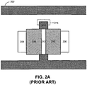
- hammer heads In order to compensate for line end shortening, designers often add optical proximity correction (OPC) features, such as "hammer heads," onto line ends. For example, in FIG. 2A , a hammerhead 215 is added onto an endcap 216 of a transistor in order to reduce the problem of line end shortening in some situations. However, note that hammerhead 215 may give rise the design rule violations that can potentially cause bridging between the hammerhead and polysilicon line 202.
- OPC optical proximity correction
- This bridging problem can be alleviated by introducing a separation between hammerhead 215 and polysilicon line 202.
- introducing such a separation increases the size of the circuit element, which means that fewer circuit elements can be integrated into a semiconductor chip.
- the invention provides a method according to claim 1, and an apparatus according to claim 9.
- One embodiment of the invention provides a system and a method for reducing line end shortening and improved gate critical dimension control during an optical lithography process for manufacturing an integrated circuit.
- the system operates by receiving a specification of the integrated circuit, wherein the specification defines transistors that include gates.
- the system identifies a gate within the specification, wherein the gate includes an endcap that is susceptible to line end shortening during the optical lithography process.
- the system then extends a phase shifter used to form the gate, so that the phase shifter defines at least a portion of the endcap and thereby reduces line end shortening of the endcap due to optical effects.
- the system replaces the endcap, which has been modified through optical proximity correction (OPC), with an (ideal) unmodified endcap.
- OPC optical proximity correction
- extending the phase shifter involves extending the phase shifter past the endcap.
- extending the phase shifter involves extending the phase shifter so that it covers at least part of the endcap, but does not extend past the endcap. In a variation on this embodiment, the phase shifter extends past the endcap.
- the system automatically checks design rules that specify a minimum distance between the phase shifter and other structures within the integrated circuit.
- the system additionally marks the endcap to prevent subsequent optical proximity correction (OPC) of the endcap.
- OPC optical proximity correction
- the system subsequently applies OPC to the layout, without applying OPC to endcaps that have been marked.
- the system replaces the endcap with a straight endcap.
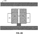
- FIG. 2B illustrates the use of an extended phase shifter to alleviate the line end shortening problem in accordance with an embodiment of the invention.
- the circuit layout in FIG. 2B is the same as the circuit layout FIG. 2A , except that the phase shifter comprised of, zero-degree clear region 208, chromium regulator 212 and 180-degree clear region 210, has been extended so that it covers at least part of endcap 216 (illustrated in FIG. 2A ).
- phase shifter may extend past endcap 216 if the phase shifter does not interfere with other features in the circuit. Otherwise, the phase shifter may extend to cover at least part of endcap 216, but not past endcap 216, so that the phase shifter defines at least a portion of the boundary of endcap 216.
- FIG. 3 illustrates the replacement of endcaps that are not straight or endcaps that have been modified with straight unmodified endcaps in accordance with an embodiment of the invention.
- a number of polysilicon lines 304-307 form a set of pass transistors in active diffusion region 302. Some of these polysilicon lines, such as polysilicon lines 304 and 307, have endcaps with OPC features that are become unnecessary if there exists an extended phase shifter. Other polysilicon lines, 305 and 306, are not straight.
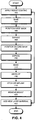
- FIG. 4 is a flow chart illustrating the wafer fabrication process in accordance with an embodiment of the invention.
- the system starts by applying the resist coating to the top surface of a wafer (step 402).
- the system bakes the resist layer (step 404).
- the system positions the first mask over the photoresist layer (step 406), and then exposes the photoresist layer through the first mask (step 408).
- the system positions the second mask over the photoresist layer (step 410), and then exposes the photoresist layer through the second mask (step 412).
- the first mask and/or the second mask may include phase shifters.
- the system then bakes the wafer again (step 414) before developing the photoresist layer (step 416).
- step 416 either a chemical etching or ion implantation step takes place (step 418) before the photoresist layer is removed (step 420).
- step 428 a new layer of material can be added and the process can be repeated for the new layer (step 422).
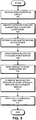
- FIG. 5 is a flow chart illustrating the process of extending a phase shifter to alleviate the line end shortening problem for a transistor endcap in accordance with an embodiment of the invention.
- the process starts when the system receives a specification of the circuit in some format, such as GDSII stream format (step 502).
- the system identifies gates within transistors that have endcaps that the designer desires to apply phase shifting to, and that are susceptible to line end shortening problems (step 504).
- phase shifters beyond the active region for example in FIG. 2B past active diffusion regions 204 and 206 (step 506). Note that this may involve extending the phase shifter beyond the endcap, which in some cases is preferable, or alternatively, extending the phase shifter to cover part or all of the endcap without extending beyond the endcap. Also note that in one embodiment of the invention, extended phase shifters can be inserted into areas that were not originally targeted for phase shifting in order to alleviate the line end shortening problem.
- the system checks design rules to ensure that there exists a pre-specified minimum distance between the extended shifter and other polysilicon features in the circuit (step 508). If a design rule violation is detected, an error can be generated, and corrective action can be taken by either modifying the polysilicon feature or by modifying the extended shifter.
- the system also marks the identified endcaps to ensure that the endcaps are not modified during a subsequent OPC process (step 510).
- an identified endcap has been modified to include an OPC feature or if the endcap is not straight, the endcap is replaced with a unmodified straight endcap as is illustrated in FIG. 3 (step 512).
- a computer readable storage medium which may be any device or medium that can store code and/or data for use by a computer system.
- the transmission medium may include a communications network, such as the Internet.
Landscapes
- Physics & Mathematics (AREA)
- General Physics & Mathematics (AREA)
- Preparing Plates And Mask In Photomechanical Process (AREA)
- Semiconductor Integrated Circuits (AREA)
- Exposure And Positioning Against Photoresist Photosensitive Materials (AREA)
- Design And Manufacture Of Integrated Circuits (AREA)
- Amplifiers (AREA)
- Microwave Amplifiers (AREA)
Claims (12)
- Verfahren zum Vermindern von Linienendverkürzung ("line end shortening") während eines optischen Lithographievorganges für die Herstellung eines integrierten Schaltkreises, welches aufweist:Empfangen einer Spezifizierung des integrierten Schaltkreises (502), wobei die Spezifizierung Transistoren definiert, die Gates aufweisen,Identifizieren eines Gates in einer Spezifizierung (504), wobei das Gate eine Endkappe aufweist, die während eines optischen Lithographievorganges der Gefahr einer Linienendverkürzung ausgesetzt ist, undErweitern eines Phasenschiebers, der verwendet wird, um das Gate über einen zugehörigen aktiven Bereich (506) hinaus zu bilden, sodass der Phasenschieber zumindest einen Teil der Endkappe definiert und dadurch die Linienendverkürzung der Endkappe aufgrund von optischen Effekten vermindert, gekennzeichnet durchEntfernen der Modifikationen an der Endkappe, die zuvor für eine optische Nahbereichskorrektur (OPC) (512) vorgenommen wurden.
- Verfahren nach Anspruch 1, wobei das Erweitern bzw. Ausdehnen des Phasenschiebers das Ausdehnen des Phasenschiebers über die Endkappe hinaus umfasst.
- Verfahren nach Anspruch 1, wobei das Ausfahren des Phasenschiebers das Ausdehnen des Phasenverschiebers in der Weise aufweist, dass er zumindest einen Teil der Endkappe abdeckt, sich jedoch nicht über die Endkappe hinaus erstreckt
- Verfahren nach einem der vorstehenden Ansprüche, weicher das automatische Überprüfen von Auslegungsregeln aufweist, welche einen minimalen Abstand zwischen dem Phasenschieber und anderen Strukturen innerhalb des integrierten Schaltkreises (508) angibt.
- Verfahren nach einem der vorstehenden Ansprüche, welches weiterhin das Markieren der Endkappe aufweist, um eine anschließende optische Nahbereichskorrektur (EPC) der Endkappe (510) zu vermeiden.
- Verfahren nach Anspruch 5, welches weiterhin das Anwenden einer optischen Nahbereichskorrektur (OPC) für die Spezifizierung des integrierten Schaltkreises aufweist, wobei die optische Nahbereichskorrektur nicht auf markierte Endkappen angewendet wird
- Verfahren nach einem der vorstehenden Ansprüche, welches weiterhin aufweist, dass dann, wenn die Endkappe nicht gerade ist, die Endkappe durch eine gerade Endkappe ersetzt wird.
- Verfahren zum Herstellen eines integrierten Schaltkreises, welches das Verfahren nach einem der Ansprüche 1 bis 7 aufweist.
- Vorrichtung zum Vermindern der Linienendverkürzung (line end shortening) während eines optischen Lithographievorganges für die Herstellung eines integrierten Schaltkreises durch Entfernen von verbliebenen optischen Nahbereichskorrekturen auf den Endkappen von Transistorgates, wobei die Vorrichtung aufweist:Einrichtungen zum Identifizieren eines Transistorgates in einem Layout bzw. Schaltplan, wobei das Transistorgate einen aktiven Bereich und eine Endkappe aufweist, wobei der aktive Bereich unter Verwendung von zumindest einem Phasenschieber definiert wird und die Endkappe zumindest eine optische Nahbereichskorrektur aufweist, undEinrichtungen zum Ausdehnen bzw. Erweitern des zumindest einen Phasenschiebers, sodass er zumindest einen Teil der Endkappe definiert,gekennzeichnet durch Einrichtungen zum Modifizieren der Endkappe um die zumindest eine optische Nahbereichskorrektur zu entfernen.
- Vorrichtung nach Anspruch 9, weiche weiterhin eine Einrichtung zum automatischen Überprüfen von Auslegungsregeln aufweist, welche einen minimalen Abstand zwischen dem zumindest einen Phasenschieber und anderen Strukturen innerhalb des Layouts angeben.
- Vorrichtung nach Anspruch 9 oder 10, welche weiterhin eine Einrichtung für das Markieren der Endkappe aufweist, um eine nachfolgende optische Nahbereichskorrektur der Endkappe zu vermeiden
- Vorrichtung nach Anspruch 11, welche weiterhin eine Einrichtung zum Anwenden einer optischen Nahbereichskorrektur (OPC) auf eine Spezifizierung des Layouts aufweist, wobei die OPC nicht auf Endkappen angewendet wird, welche markiert worden sind.
Applications Claiming Priority (5)
| Application Number | Priority Date | Filing Date | Title |
|---|---|---|---|
| US872620 | 1986-06-10 | ||
| US28132501P | 2001-04-03 | 2001-04-03 | |
| US281325P | 2001-04-03 | ||
| US09/872,620 US6553560B2 (en) | 2001-04-03 | 2001-05-31 | Alleviating line end shortening in transistor endcaps by extending phase shifters |
| PCT/US2002/004119 WO2002082182A2 (en) | 2001-04-03 | 2002-02-11 | Alleviating line end shortening in transistor endcaps by extending phase shifters |
Publications (2)
| Publication Number | Publication Date |
|---|---|
| EP1410105A2 EP1410105A2 (de) | 2004-04-21 |
| EP1410105B1 true EP1410105B1 (de) | 2012-05-02 |
Family
ID=26960832
Family Applications (1)
| Application Number | Title | Priority Date | Filing Date |
|---|---|---|---|
| EP02709485A Expired - Lifetime EP1410105B1 (de) | 2001-04-03 | 2002-02-11 | Vermeidung der schrumpfung von linienenden bei transistoren durch zusätzliche phasenschiebermuster |
Country Status (7)
| Country | Link |
|---|---|
| US (2) | US6553560B2 (de) |
| EP (1) | EP1410105B1 (de) |
| JP (2) | JP4700898B2 (de) |
| AT (1) | ATE556354T1 (de) |
| AU (1) | AU2002243967A1 (de) |
| TW (1) | TW521322B (de) |
| WO (1) | WO2002082182A2 (de) |
Cited By (1)
| Publication number | Priority date | Publication date | Assignee | Title |
|---|---|---|---|---|
| US9418935B1 (en) | 2015-09-09 | 2016-08-16 | Globalfoundries Inc. | Integrated circuit line ends formed using additive processing |
Families Citing this family (30)
| Publication number | Priority date | Publication date | Assignee | Title |
|---|---|---|---|---|
| US6787271B2 (en) * | 2000-07-05 | 2004-09-07 | Numerical Technologies, Inc. | Design and layout of phase shifting photolithographic masks |
| US7083879B2 (en) | 2001-06-08 | 2006-08-01 | Synopsys, Inc. | Phase conflict resolution for photolithographic masks |
| US6866971B2 (en) | 2000-09-26 | 2005-03-15 | Synopsys, Inc. | Full phase shifting mask in damascene process |
| US6573010B2 (en) | 2001-04-03 | 2003-06-03 | Numerical Technologies, Inc. | Method and apparatus for reducing incidental exposure by using a phase shifter with a variable regulator |
| US6553560B2 (en) * | 2001-04-03 | 2003-04-22 | Numerical Technologies, Inc. | Alleviating line end shortening in transistor endcaps by extending phase shifters |
| US6566019B2 (en) | 2001-04-03 | 2003-05-20 | Numerical Technologies, Inc. | Using double exposure effects during phase shifting to control line end shortening |
| US6593038B2 (en) | 2001-05-04 | 2003-07-15 | Numerical Technologies, Inc. | Method and apparatus for reducing color conflicts during trim generation for phase shifters |
| US6569583B2 (en) | 2001-05-04 | 2003-05-27 | Numerical Technologies, Inc. | Method and apparatus for using phase shifter cutbacks to resolve phase shifter conflicts |
| US6852471B2 (en) * | 2001-06-08 | 2005-02-08 | Numerical Technologies, Inc. | Exposure control for phase shifting photolithographic masks |
| US7178128B2 (en) * | 2001-07-13 | 2007-02-13 | Synopsys Inc. | Alternating phase shift mask design conflict resolution |
| US6664009B2 (en) | 2001-07-27 | 2003-12-16 | Numerical Technologies, Inc. | Method and apparatus for allowing phase conflicts in phase shifting mask and chromeless phase edges |
| US6738958B2 (en) | 2001-09-10 | 2004-05-18 | Numerical Technologies, Inc. | Modifying a hierarchical representation of a circuit to process composite gates |
| US6698007B2 (en) | 2001-10-09 | 2004-02-24 | Numerical Technologies, Inc. | Method and apparatus for resolving coloring conflicts between phase shifters |
| US7122281B2 (en) | 2002-02-26 | 2006-10-17 | Synopsys, Inc. | Critical dimension control using full phase and trim masks |
| US6605481B1 (en) | 2002-03-08 | 2003-08-12 | Numerical Technologies, Inc. | Facilitating an adjustable level of phase shifting during an optical lithography process for manufacturing an integrated circuit |
| US6944844B2 (en) * | 2002-04-03 | 2005-09-13 | Synopsys, Inc. | System and method to determine impact of line end shortening |
| US6704921B2 (en) | 2002-04-03 | 2004-03-09 | Numerical Technologies, Inc. | Automated flow in PSM phase assignment |
| US6785879B2 (en) * | 2002-06-11 | 2004-08-31 | Numerical Technologies, Inc. | Model-based data conversion |
| US6711732B1 (en) * | 2002-07-26 | 2004-03-23 | Taiwan Semiconductor Manufacturing Company | Full sized scattering bar alt-PSM technique for IC manufacturing in sub-resolution era |
| US6821689B2 (en) | 2002-09-16 | 2004-11-23 | Numerical Technologies | Using second exposure to assist a PSM exposure in printing a tight space adjacent to large feature |
| US7448012B1 (en) | 2004-04-21 | 2008-11-04 | Qi-De Qian | Methods and system for improving integrated circuit layout |
| US7445874B2 (en) * | 2004-11-10 | 2008-11-04 | Chartered Semiconductor Manufacturing, Ltd | Method to resolve line end distortion for alternating phase shift mask |
| US7617473B2 (en) | 2005-01-21 | 2009-11-10 | International Business Machines Corporation | Differential alternating phase shift mask optimization |
| US20060257795A1 (en) * | 2005-05-16 | 2006-11-16 | Benjamin Szu-Min Lin | Method for forming composite pattern including different types of patterns |
| US7491343B2 (en) * | 2006-09-14 | 2009-02-17 | Lam Research Corporation | Line end shortening reduction during etch |
| US7407597B2 (en) * | 2006-09-14 | 2008-08-05 | Lam Research Corporation | Line end shortening reduction during etch |
| US7713824B2 (en) | 2007-02-21 | 2010-05-11 | Infineon Technologies North America Corp. | Small feature integrated circuit fabrication |
| CN103105727B (zh) * | 2011-11-15 | 2014-06-04 | 无锡华润上华科技有限公司 | 形成光掩膜版的方法及光掩膜版 |
| US8856695B1 (en) | 2013-03-14 | 2014-10-07 | Samsung Electronics Co., Ltd. | Method for generating post-OPC layout in consideration of top loss of etch mask layer |
| KR102279711B1 (ko) | 2014-03-11 | 2021-07-21 | 삼성전자주식회사 | 반도체 장치의 레이아웃 방법, 포토 마스크 및 이를 이용하여 제조된 반도체 장치 |
Family Cites Families (73)
| Publication number | Priority date | Publication date | Assignee | Title |
|---|---|---|---|---|
| US4456371A (en) | 1982-06-30 | 1984-06-26 | International Business Machines Corporation | Optical projection printing threshold leveling arrangement |
| JPH0690505B2 (ja) | 1985-09-20 | 1994-11-14 | 株式会社日立製作所 | ホトマスク |
| JP2650962B2 (ja) | 1988-05-11 | 1997-09-10 | 株式会社日立製作所 | 露光方法及び素子の形成方法並びに半導体素子の製造方法 |
| JP2710967B2 (ja) | 1988-11-22 | 1998-02-10 | 株式会社日立製作所 | 集積回路装置の製造方法 |
| JP2862183B2 (ja) | 1989-04-28 | 1999-02-24 | 富士通株式会社 | マスクの製造方法 |
| US5328807A (en) | 1990-06-11 | 1994-07-12 | Hitichi, Ltd. | Method of forming a pattern |
| JP2974821B2 (ja) | 1991-06-19 | 1999-11-10 | 沖電気工業株式会社 | パターン形成方法 |
| KR100256619B1 (ko) | 1991-07-12 | 2000-06-01 | 사와무라 시코 | 포토마스크 및 그것을 사용한 레지시트 패턴 형성방법 |
| US5364716A (en) | 1991-09-27 | 1994-11-15 | Fujitsu Limited | Pattern exposing method using phase shift and mask used therefor |
| JP3148770B2 (ja) | 1992-03-27 | 2001-03-26 | 日本電信電話株式会社 | ホトマスク及びマスクパタンデータ処理方法 |
| US5308741A (en) | 1992-07-31 | 1994-05-03 | Motorola, Inc. | Lithographic method using double exposure techniques, mask position shifting and light phase shifting |
| US5302477A (en) | 1992-08-21 | 1994-04-12 | Intel Corporation | Inverted phase-shifted reticle |
| US5538815A (en) | 1992-09-14 | 1996-07-23 | Kabushiki Kaisha Toshiba | Method for designing phase-shifting masks with automatization capability |
| US5527645A (en) | 1993-04-21 | 1996-06-18 | Pati; Yagyensh C. | Systematic method for production of phase-shifting photolithographic masks |
| JPH07111528A (ja) | 1993-10-12 | 1995-04-25 | Matsushita Electric Ind Co Ltd | 留守番電話装置 |
| US5424154A (en) | 1993-12-10 | 1995-06-13 | Intel Corporation | Lithographic emhancement method and apparatus for randomly spaced structures |
| JP3393926B2 (ja) | 1993-12-28 | 2003-04-07 | 株式会社東芝 | フォトマスク設計方法及びその装置 |
| EP0674223B1 (de) | 1994-02-14 | 1997-05-02 | International Business Machines Corporation | Dämpfende Phasenverschiebungsmaske und Herstellungsverfahren |
| US5573890A (en) | 1994-07-18 | 1996-11-12 | Advanced Micro Devices, Inc. | Method of optical lithography using phase shift masking |
| US5538833A (en) | 1994-08-03 | 1996-07-23 | International Business Machines Corporation | High resolution phase edge lithography without the need for a trim mask |
| US5537648A (en) | 1994-08-15 | 1996-07-16 | International Business Machines Corporation | Geometric autogeneration of "hard" phase-shift designs for VLSI |
| US5472814A (en) | 1994-11-17 | 1995-12-05 | International Business Machines Corporation | Orthogonally separated phase shifted and unphase shifted mask patterns for image improvement |
| US5565286A (en) | 1994-11-17 | 1996-10-15 | International Business Machines Corporation | Combined attenuated-alternating phase shifting mask structure and fabrication methods therefor |
| KR0158904B1 (ko) | 1994-12-02 | 1999-02-01 | 김주용 | 콘택마스크 |
| US5523186A (en) | 1994-12-16 | 1996-06-04 | International Business Machines Corporation | Split and cover technique for phase shifting photolithography |
| JP3273456B2 (ja) | 1995-02-24 | 2002-04-08 | アルプス電気株式会社 | モータ駆動スライド型可変抵抗器 |
| US5532090A (en) | 1995-03-01 | 1996-07-02 | Intel Corporation | Method and apparatus for enhanced contact and via lithography |
| US5595843A (en) | 1995-03-30 | 1997-01-21 | Intel Corporation | Layout methodology, mask set, and patterning method for phase-shifting lithography |
| JP2638561B2 (ja) | 1995-05-10 | 1997-08-06 | 株式会社日立製作所 | マスク形成方法 |
| KR0161879B1 (ko) | 1995-09-25 | 1999-01-15 | 문정환 | 위상 반전 마스크의 구조 및 제조방법 |
| JP2917879B2 (ja) | 1995-10-31 | 1999-07-12 | 日本電気株式会社 | フォトマスク及びその製造方法 |
| US6185727B1 (en) | 1995-12-12 | 2001-02-06 | International Business Machines Corporation | Design verification for asymmetric phase shift mask layouts |
| US5885734A (en) | 1996-08-15 | 1999-03-23 | Micron Technology, Inc. | Process for modifying a hierarchical mask layout |
| US5994002A (en) | 1996-09-06 | 1999-11-30 | Matsushita Electric Industrial Co., Ltd. | Photo mask and pattern forming method |
| JP3518275B2 (ja) | 1996-09-06 | 2004-04-12 | 松下電器産業株式会社 | フォトマスクおよびパターン形成方法 |
| PT927381E (pt) | 1996-09-18 | 2004-10-29 | Numerical Tech Inc | Metodo e dispositivo de producao de circuitos de mudanca de fase |
| US6228539B1 (en) | 1996-09-18 | 2001-05-08 | Numerical Technologies, Inc. | Phase shifting circuit manufacture method and apparatus |
| US5858580A (en) | 1997-09-17 | 1999-01-12 | Numerical Technologies, Inc. | Phase shifting circuit manufacture method and apparatus |
| US5923562A (en) | 1996-10-18 | 1999-07-13 | International Business Machines Corporation | Method for automatically eliminating three way intersection design conflicts in phase edge, phase shift designs |
| US5807649A (en) | 1996-10-31 | 1998-09-15 | International Business Machines Corporation | Lithographic patterning method and mask set therefor with light field trim mask |
| JPH10207038A (ja) | 1997-01-28 | 1998-08-07 | Matsushita Electric Ind Co Ltd | レチクル及びパターン形成方法 |
| US5883813A (en) | 1997-03-04 | 1999-03-16 | International Business Machines Corporation | Automatic generation of phase shift masks using net coloring |
| US5923566A (en) | 1997-03-25 | 1999-07-13 | International Business Machines Corporation | Phase shifted design verification routine |
| US6057063A (en) | 1997-04-14 | 2000-05-02 | International Business Machines Corporation | Phase shifted mask design system, phase shifted mask and VLSI circuit devices manufactured therewith |
| US6370679B1 (en) * | 1997-09-17 | 2002-04-09 | Numerical Technologies, Inc. | Data hierarchy layout correction and verification method and apparatus |
| US6470489B1 (en) * | 1997-09-17 | 2002-10-22 | Numerical Technologies, Inc. | Design rule checking system and method |
| JP3101594B2 (ja) | 1997-11-06 | 2000-10-23 | キヤノン株式会社 | 露光方法及び露光装置 |
| TW363147B (en) | 1997-11-22 | 1999-07-01 | United Microelectronics Corp | Phase shifting mask |
| TW378281B (en) | 1997-11-28 | 2000-01-01 | United Microelectronics Corp | Phase shift mask and method for manufacturing the same |
| US6083275A (en) | 1998-01-09 | 2000-07-04 | International Business Machines Corporation | Optimized phase shift design migration |
| JP3307313B2 (ja) | 1998-01-23 | 2002-07-24 | ソニー株式会社 | パターン生成方法及びその装置 |
| JP4019491B2 (ja) * | 1998-03-30 | 2007-12-12 | ソニー株式会社 | 露光方法 |
| US6189136B1 (en) * | 1998-07-20 | 2001-02-13 | Philips Electronics, North America Corp. | Design level optical proximity correction methods |
| US6130012A (en) | 1999-01-13 | 2000-10-10 | Advanced Micro Devices, Inc. | Ion beam milling to generate custom reticles |
| JP3482172B2 (ja) * | 1999-03-04 | 2003-12-22 | 松下電器産業株式会社 | Lsi用パターンのレイアウト作成方法及びlsi用パターンの形成方法 |
| US6139994A (en) | 1999-06-25 | 2000-10-31 | Broeke; Doug Van Den | Use of intersecting subresolution features for microlithography |
| US6251549B1 (en) | 1999-07-19 | 2001-06-26 | Marc David Levenson | Generic phase shift mask |
| US6335128B1 (en) | 1999-09-28 | 2002-01-01 | Nicolas Bailey Cobb | Method and apparatus for determining phase shifts and trim masks for an integrated circuit |
| US6338922B1 (en) | 2000-05-08 | 2002-01-15 | International Business Machines Corporation | Optimized alternating phase shifted mask design |
| US6978436B2 (en) | 2000-07-05 | 2005-12-20 | Synopsys, Inc. | Design data format and hierarchy management for phase processing |
| US6733929B2 (en) | 2000-07-05 | 2004-05-11 | Numerical Technologies, Inc. | Phase shift masking for complex patterns with proximity adjustments |
| US6524752B1 (en) * | 2000-07-05 | 2003-02-25 | Numerical Technologies, Inc. | Phase shift masking for intersecting lines |
| US6503666B1 (en) | 2000-07-05 | 2003-01-07 | Numerical Technologies, Inc. | Phase shift masking for complex patterns |
| US6681379B2 (en) | 2000-07-05 | 2004-01-20 | Numerical Technologies, Inc. | Phase shifting design and layout for static random access memory |
| US7028285B2 (en) | 2000-07-05 | 2006-04-11 | Synopsys, Inc. | Standard cell design incorporating phase information |
| US6430737B1 (en) * | 2000-07-10 | 2002-08-06 | Mentor Graphics Corp. | Convergence technique for model-based optical and process correction |
| US6901575B2 (en) | 2000-10-25 | 2005-05-31 | Numerical Technologies, Inc. | Resolving phase-shift conflicts in layouts using weighted links between phase shifters |
| EP1370909A1 (de) | 2001-03-08 | 2003-12-17 | Numerical Technologies, Inc. | Alternierende phasenschiebermaske für variierende strukturauflösungen |
| US6635393B2 (en) | 2001-03-23 | 2003-10-21 | Numerical Technologies, Inc. | Blank for alternating PSM photomask with charge dissipation layer |
| US6566019B2 (en) | 2001-04-03 | 2003-05-20 | Numerical Technologies, Inc. | Using double exposure effects during phase shifting to control line end shortening |
| US6573010B2 (en) | 2001-04-03 | 2003-06-03 | Numerical Technologies, Inc. | Method and apparatus for reducing incidental exposure by using a phase shifter with a variable regulator |
| US6553560B2 (en) | 2001-04-03 | 2003-04-22 | Numerical Technologies, Inc. | Alleviating line end shortening in transistor endcaps by extending phase shifters |
| US6728912B2 (en) * | 2001-04-12 | 2004-04-27 | International Business Machines Corporation | SOI cell stability test method |
-
2001
- 2001-05-31 US US09/872,620 patent/US6553560B2/en not_active Expired - Lifetime
-
2002
- 2002-02-11 AU AU2002243967A patent/AU2002243967A1/en not_active Abandoned
- 2002-02-11 EP EP02709485A patent/EP1410105B1/de not_active Expired - Lifetime
- 2002-02-11 JP JP2002579888A patent/JP4700898B2/ja not_active Expired - Lifetime
- 2002-02-11 WO PCT/US2002/004119 patent/WO2002082182A2/en not_active Ceased
- 2002-02-11 AT AT02709485T patent/ATE556354T1/de active
- 2002-02-25 TW TW091103328A patent/TW521322B/zh not_active IP Right Cessation
- 2002-12-06 US US10/313,325 patent/US6859918B2/en not_active Expired - Lifetime
-
2009
- 2009-08-11 JP JP2009186919A patent/JP2009271550A/ja not_active Withdrawn
Cited By (1)
| Publication number | Priority date | Publication date | Assignee | Title |
|---|---|---|---|---|
| US9418935B1 (en) | 2015-09-09 | 2016-08-16 | Globalfoundries Inc. | Integrated circuit line ends formed using additive processing |
Also Published As
| Publication number | Publication date |
|---|---|
| WO2002082182A3 (en) | 2004-02-19 |
| JP4700898B2 (ja) | 2011-06-15 |
| JP2004527790A (ja) | 2004-09-09 |
| US6859918B2 (en) | 2005-02-22 |
| ATE556354T1 (de) | 2012-05-15 |
| US20020144232A1 (en) | 2002-10-03 |
| US20030066038A1 (en) | 2003-04-03 |
| TW521322B (en) | 2003-02-21 |
| WO2002082182A2 (en) | 2002-10-17 |
| EP1410105A2 (de) | 2004-04-21 |
| US6553560B2 (en) | 2003-04-22 |
| AU2002243967A1 (en) | 2002-10-21 |
| JP2009271550A (ja) | 2009-11-19 |
Similar Documents
| Publication | Publication Date | Title |
|---|---|---|
| EP1410105B1 (de) | Vermeidung der schrumpfung von linienenden bei transistoren durch zusätzliche phasenschiebermuster | |
| US6566019B2 (en) | Using double exposure effects during phase shifting to control line end shortening | |
| US7036108B2 (en) | Full sized scattering bar alt-PSM technique for IC manufacturing in sub-resolution era | |
| US7585600B2 (en) | Method and apparatus for performing target-image-based optical proximity correction | |
| US6573010B2 (en) | Method and apparatus for reducing incidental exposure by using a phase shifter with a variable regulator | |
| US6821689B2 (en) | Using second exposure to assist a PSM exposure in printing a tight space adjacent to large feature | |
| US6569583B2 (en) | Method and apparatus for using phase shifter cutbacks to resolve phase shifter conflicts | |
| US6632576B2 (en) | Optical assist feature for two-mask exposure lithography | |
| US6808850B2 (en) | Performing optical proximity correction on trim-level segments not abutting features to be printed | |
| US6593038B2 (en) | Method and apparatus for reducing color conflicts during trim generation for phase shifters | |
| US6813759B2 (en) | Hybrid optical proximity correction for alternating aperture phase shifting designs | |
| US6797441B2 (en) | Method and apparatus for using a complementary mask to clear phase conflicts on a phase shifting mask | |
| KR100434707B1 (ko) | 반도체 소자 제조용 노광 마스크 | |
| US7615318B2 (en) | Printing of design features using alternating PSM technology with double mask exposure strategy |
Legal Events
| Date | Code | Title | Description |
|---|---|---|---|
| PUAI | Public reference made under article 153(3) epc to a published international application that has entered the european phase |
Free format text: ORIGINAL CODE: 0009012 |
|
| 17P | Request for examination filed |
Effective date: 20030923 |
|
| AK | Designated contracting states |
Kind code of ref document: A2 Designated state(s): AT BE CH CY DE DK ES FI FR GB GR IE IT LI LU MC NL PT SE TR |
|
| AX | Request for extension of the european patent |
Extension state: AL LT LV MK RO SI |
|
| RAP1 | Party data changed (applicant data changed or rights of an application transferred) |
Owner name: SYNOPSYS MERGER HOLDINGS LLC |
|
| RAP1 | Party data changed (applicant data changed or rights of an application transferred) |
Owner name: SYNOPSYS, INC. |
|
| 17Q | First examination report despatched |
Effective date: 20100203 |
|
| GRAP | Despatch of communication of intention to grant a patent |
Free format text: ORIGINAL CODE: EPIDOSNIGR1 |
|
| GRAS | Grant fee paid |
Free format text: ORIGINAL CODE: EPIDOSNIGR3 |
|
| REG | Reference to a national code |
Ref country code: DE Ref legal event code: R079 Ref document number: 60242798 Country of ref document: DE Free format text: PREVIOUS MAIN CLASS: G03F0001000000 Ipc: G03F0001300000 |
|
| GRAA | (expected) grant |
Free format text: ORIGINAL CODE: 0009210 |
|
| AK | Designated contracting states |
Kind code of ref document: B1 Designated state(s): AT BE CH CY DE DK ES FI FR GB GR IE IT LI LU MC NL PT SE TR |
|
| REG | Reference to a national code |
Ref country code: GB Ref legal event code: FG4D |
|
| RIC1 | Information provided on ipc code assigned before grant |
Ipc: H01L 21/28 20060101ALI20120328BHEP Ipc: G03F 1/36 20120101ALI20120328BHEP Ipc: G03F 1/30 20120101AFI20120328BHEP |
|
| REG | Reference to a national code |
Ref country code: AT Ref legal event code: REF Ref document number: 556354 Country of ref document: AT Kind code of ref document: T Effective date: 20120515 Ref country code: CH Ref legal event code: EP |
|
| REG | Reference to a national code |
Ref country code: IE Ref legal event code: FG4D |
|
| REG | Reference to a national code |
Ref country code: DE Ref legal event code: R096 Ref document number: 60242798 Country of ref document: DE Effective date: 20120705 |
|
| REG | Reference to a national code |
Ref country code: NL Ref legal event code: VDEP Effective date: 20120502 |
|
| PG25 | Lapsed in a contracting state [announced via postgrant information from national office to epo] |
Ref country code: FI Free format text: LAPSE BECAUSE OF FAILURE TO SUBMIT A TRANSLATION OF THE DESCRIPTION OR TO PAY THE FEE WITHIN THE PRESCRIBED TIME-LIMIT Effective date: 20120502 Ref country code: SE Free format text: LAPSE BECAUSE OF FAILURE TO SUBMIT A TRANSLATION OF THE DESCRIPTION OR TO PAY THE FEE WITHIN THE PRESCRIBED TIME-LIMIT Effective date: 20120502 Ref country code: CY Free format text: LAPSE BECAUSE OF FAILURE TO SUBMIT A TRANSLATION OF THE DESCRIPTION OR TO PAY THE FEE WITHIN THE PRESCRIBED TIME-LIMIT Effective date: 20120502 |
|
| REG | Reference to a national code |
Ref country code: AT Ref legal event code: MK05 Ref document number: 556354 Country of ref document: AT Kind code of ref document: T Effective date: 20120502 |
|
| PG25 | Lapsed in a contracting state [announced via postgrant information from national office to epo] |
Ref country code: GR Free format text: LAPSE BECAUSE OF FAILURE TO SUBMIT A TRANSLATION OF THE DESCRIPTION OR TO PAY THE FEE WITHIN THE PRESCRIBED TIME-LIMIT Effective date: 20120803 Ref country code: PT Free format text: LAPSE BECAUSE OF FAILURE TO SUBMIT A TRANSLATION OF THE DESCRIPTION OR TO PAY THE FEE WITHIN THE PRESCRIBED TIME-LIMIT Effective date: 20120903 |
|
| PG25 | Lapsed in a contracting state [announced via postgrant information from national office to epo] |
Ref country code: BE Free format text: LAPSE BECAUSE OF FAILURE TO SUBMIT A TRANSLATION OF THE DESCRIPTION OR TO PAY THE FEE WITHIN THE PRESCRIBED TIME-LIMIT Effective date: 20120502 |
|
| PG25 | Lapsed in a contracting state [announced via postgrant information from national office to epo] |
Ref country code: AT Free format text: LAPSE BECAUSE OF FAILURE TO SUBMIT A TRANSLATION OF THE DESCRIPTION OR TO PAY THE FEE WITHIN THE PRESCRIBED TIME-LIMIT Effective date: 20120502 Ref country code: NL Free format text: LAPSE BECAUSE OF FAILURE TO SUBMIT A TRANSLATION OF THE DESCRIPTION OR TO PAY THE FEE WITHIN THE PRESCRIBED TIME-LIMIT Effective date: 20120502 Ref country code: DK Free format text: LAPSE BECAUSE OF FAILURE TO SUBMIT A TRANSLATION OF THE DESCRIPTION OR TO PAY THE FEE WITHIN THE PRESCRIBED TIME-LIMIT Effective date: 20120502 |
|
| PG25 | Lapsed in a contracting state [announced via postgrant information from national office to epo] |
Ref country code: IT Free format text: LAPSE BECAUSE OF FAILURE TO SUBMIT A TRANSLATION OF THE DESCRIPTION OR TO PAY THE FEE WITHIN THE PRESCRIBED TIME-LIMIT Effective date: 20120502 |
|
| PLBE | No opposition filed within time limit |
Free format text: ORIGINAL CODE: 0009261 |
|
| STAA | Information on the status of an ep patent application or granted ep patent |
Free format text: STATUS: NO OPPOSITION FILED WITHIN TIME LIMIT |
|
| 26N | No opposition filed |
Effective date: 20130205 |
|
| PG25 | Lapsed in a contracting state [announced via postgrant information from national office to epo] |
Ref country code: ES Free format text: LAPSE BECAUSE OF FAILURE TO SUBMIT A TRANSLATION OF THE DESCRIPTION OR TO PAY THE FEE WITHIN THE PRESCRIBED TIME-LIMIT Effective date: 20120813 |
|
| REG | Reference to a national code |
Ref country code: DE Ref legal event code: R097 Ref document number: 60242798 Country of ref document: DE Effective date: 20130205 |
|
| PG25 | Lapsed in a contracting state [announced via postgrant information from national office to epo] |
Ref country code: MC Free format text: LAPSE BECAUSE OF NON-PAYMENT OF DUE FEES Effective date: 20130228 |
|
| REG | Reference to a national code |
Ref country code: CH Ref legal event code: PL |
|
| PG25 | Lapsed in a contracting state [announced via postgrant information from national office to epo] |
Ref country code: CH Free format text: LAPSE BECAUSE OF NON-PAYMENT OF DUE FEES Effective date: 20130228 Ref country code: LI Free format text: LAPSE BECAUSE OF NON-PAYMENT OF DUE FEES Effective date: 20130228 |
|
| REG | Reference to a national code |
Ref country code: IE Ref legal event code: MM4A |
|
| PG25 | Lapsed in a contracting state [announced via postgrant information from national office to epo] |
Ref country code: IE Free format text: LAPSE BECAUSE OF NON-PAYMENT OF DUE FEES Effective date: 20130211 |
|
| REG | Reference to a national code |
Ref country code: FR Ref legal event code: PLFP Year of fee payment: 14 |
|
| PG25 | Lapsed in a contracting state [announced via postgrant information from national office to epo] |
Ref country code: TR Free format text: LAPSE BECAUSE OF FAILURE TO SUBMIT A TRANSLATION OF THE DESCRIPTION OR TO PAY THE FEE WITHIN THE PRESCRIBED TIME-LIMIT Effective date: 20120502 |
|
| PG25 | Lapsed in a contracting state [announced via postgrant information from national office to epo] |
Ref country code: LU Free format text: LAPSE BECAUSE OF NON-PAYMENT OF DUE FEES Effective date: 20130211 |
|
| REG | Reference to a national code |
Ref country code: FR Ref legal event code: PLFP Year of fee payment: 15 |
|
| REG | Reference to a national code |
Ref country code: FR Ref legal event code: PLFP Year of fee payment: 16 |
|
| REG | Reference to a national code |
Ref country code: FR Ref legal event code: PLFP Year of fee payment: 17 |
|
| PGFP | Annual fee paid to national office [announced via postgrant information from national office to epo] |
Ref country code: FR Payment date: 20210120 Year of fee payment: 20 |
|
| PGFP | Annual fee paid to national office [announced via postgrant information from national office to epo] |
Ref country code: DE Payment date: 20210120 Year of fee payment: 20 Ref country code: GB Payment date: 20210120 Year of fee payment: 20 |
|
| REG | Reference to a national code |
Ref country code: DE Ref legal event code: R071 Ref document number: 60242798 Country of ref document: DE |
|
| REG | Reference to a national code |
Ref country code: GB Ref legal event code: PE20 Expiry date: 20220210 |
|
| PG25 | Lapsed in a contracting state [announced via postgrant information from national office to epo] |
Ref country code: GB Free format text: LAPSE BECAUSE OF EXPIRATION OF PROTECTION Effective date: 20220210 |