EP1407645B1 - Electrically connecting element between a back plate and another back plate or a housing for electronic circuits - Google Patents
Electrically connecting element between a back plate and another back plate or a housing for electronic circuits Download PDFInfo
- Publication number
- EP1407645B1 EP1407645B1 EP02744059A EP02744059A EP1407645B1 EP 1407645 B1 EP1407645 B1 EP 1407645B1 EP 02744059 A EP02744059 A EP 02744059A EP 02744059 A EP02744059 A EP 02744059A EP 1407645 B1 EP1407645 B1 EP 1407645B1
- Authority
- EP
- European Patent Office
- Prior art keywords
- main portion
- back plate
- elastic
- recess
- contact element
- Prior art date
- Legal status (The legal status is an assumption and is not a legal conclusion. Google has not performed a legal analysis and makes no representation as to the accuracy of the status listed.)
- Expired - Lifetime
Links
Images


Classifications
-
- G—PHYSICS
- G06—COMPUTING OR CALCULATING; COUNTING
- G06F—ELECTRIC DIGITAL DATA PROCESSING
- G06F1/00—Details not covered by groups G06F3/00 - G06F13/00 and G06F21/00
- G06F1/16—Constructional details or arrangements
- G06F1/18—Packaging or power distribution
-
- G—PHYSICS
- G06—COMPUTING OR CALCULATING; COUNTING
- G06F—ELECTRIC DIGITAL DATA PROCESSING
- G06F1/00—Details not covered by groups G06F3/00 - G06F13/00 and G06F21/00
- G06F1/16—Constructional details or arrangements
- G06F1/18—Packaging or power distribution
- G06F1/183—Internal mounting support structures, e.g. for printed circuit boards, internal connecting means
- G06F1/185—Mounting of expansion boards
-
- G—PHYSICS
- G06—COMPUTING OR CALCULATING; COUNTING
- G06F—ELECTRIC DIGITAL DATA PROCESSING
- G06F1/00—Details not covered by groups G06F3/00 - G06F13/00 and G06F21/00
- G06F1/16—Constructional details or arrangements
- G06F1/18—Packaging or power distribution
- G06F1/183—Internal mounting support structures, e.g. for printed circuit boards, internal connecting means
- G06F1/184—Mounting of motherboards
-
- G—PHYSICS
- G06—COMPUTING OR CALCULATING; COUNTING
- G06F—ELECTRIC DIGITAL DATA PROCESSING
- G06F1/00—Details not covered by groups G06F3/00 - G06F13/00 and G06F21/00
- G06F1/16—Constructional details or arrangements
- G06F1/18—Packaging or power distribution
- G06F1/183—Internal mounting support structures, e.g. for printed circuit boards, internal connecting means
- G06F1/186—Securing of expansion boards in correspondence to slots provided at the computer enclosure
-
- H—ELECTRICITY
- H05—ELECTRIC TECHNIQUES NOT OTHERWISE PROVIDED FOR
- H05K—PRINTED CIRCUITS; CASINGS OR CONSTRUCTIONAL DETAILS OF ELECTRIC APPARATUS; MANUFACTURE OF ASSEMBLAGES OF ELECTRICAL COMPONENTS
- H05K9/00—Screening of apparatus or components against electric or magnetic fields
- H05K9/0007—Casings
- H05K9/0015—Gaskets or seals
- H05K9/0016—Gaskets or seals having a spring contact
Definitions
- the invention relates to an apparatus housing or an apparatus casing such as an apparatus box for electronic circuits including electrically shielded openings for external connection of expansion boards or insertable boards and devices for providing this electric shielding, in particular a method and a device for electrical contacting of back plates of insertable boards and a system for building frames for such back plates.
- personal computers are intended to be provided with accessories such as i.a. insertable boards or expansion boards for different functions such as typically for connection of a displaying monitor, i.e. to provide graphical displaying, for communication for instance through a modem or with a local network, for driving loudspeakers.
- the insertable boards are inserted in specially formed slot-shaped connectors that are generally directly mounted to the motherboard of the personal computer.
- the short side of an insertable board can carry connectors for a communication with the exterior and these connectors are then attached to a narrow back plate or shielding or covering plate of metal, that is mounted in an opening in the housing of the computer.
- the back plate has a bent top part that can be screwed to a frame at the opening and it is more narrow at its lower part where it can be inserted in a slot in the frame.
- simple back plates made of sheet metal are used, “dummy cover plates” or “idling cover plates”, having no connectors and having no electric connections.
- these back plates must well cover the opening in the computer box and furthermore, they must be in a good electrical contact with the material of the box. The latter condition is also true for the frame at the opening in which the back plates are attached.
- U.S. Patent No. 5,929,376 a pressed plate 12 mounted in an openings in an instrument casing 10 is disclosed.
- the plate has in turn openings for expansion boards provided with back plates.
- springs 54, 54' are provided to connect an inserted back plate to the shaped plate 12.
- the springs have contact tongues acting against a large surface of the back plates belonging to inserted boards. This has a disadvantage by the fact that a lower pressing force and thereby a worse electrical contact can be obtained at the center of the back plate, see col. 3, lines 11-16. Therefore, reinforcement rods 72 for the springs are provided.
- a housing consisting of a socket 1 for mounting it to a wall of a room and a plurality of identical frame parts that are attached to the socket and at the sides of each other and that themselves form the housing.
- the space formed in each frame part can be closed by front and rear caps 30, 28.
- the spaces are not intended for expansion boards having back plates.
- the disclosed housing is a modularly constructed housing intended to accommodate simple boards for internal connections.
- a contact spring for shielding between housing elements of electronic equipment has two legs that have different lengths and are connected by a cylindrical portion and they are bent towards each other so that a profile approximately as the figure 9 is obtained.
- the shorter leg has outermost a portion which is bent in an angle and is intended to enter an opening in a housing flange to maintain the spring in place.
- the bent portion of the spring is furthermore intended to come in mechanical and electric contact with an adjacent housing flange and then acts with a pressing force against the large surface of this flange.
- Apparatus housings having openings for expansion boards are also disclosed in U.S. Patents Nos. 5,579,210 , 5,679,923 , 5,820,171 , 4,873,395 , 5,004,867 , 4,924,355 and the published European Patent Application No. 0 723 389 .
- Contact springs for electric contact and shielding are disclosed in U.S. Patents Nos. 5,539,149 , 5,952,608 and German Patent Document 196 44 417 .
- Contact elements for an electromagnetic shielding device are disclosed in document WO93/20676 .
- a housing for electronic devices is provided, typically a computer box or box for other electronic circuits and particularly for such electronic circuits that are sensitive to external magnetic radiation, in particular high frequency electromagnetic radiation such as high frequency radio waves and microwaves.
- the housing is made from electrically conducting material, typically steel plate, and has an opening generally intended for expansion boards, for example for boards that are intended for communication of the electronic circuits with the exterior such as other remotely, located electronic circuits.
- a frame is mounted at the opening and has outer portions connecting to the edges of the opening.
- Back plates, also called shielding, protection or covering plates that can be comprised in such boards or be dummy boards or possibly only carry connectors connected through electrical lines to the electronic circuits inside the housing, are intended to be mounted in the opening.
- the back plates all have substantially the same shape including two large, approximately rectangular, identical opposite surfaces that can be elongated or strip shaped, a large inner surface and a large outer surface, and narrow longitudinal edge surfaces that at edge lines connect to the large surfaces, at two opposite edges of the large surfaces.
- the frame is divided in structural elements, a left side frame part and a right side frame part and in most cases at least one intermediate part. Thereby, the frame can be adapted to an arbitrary number of back plates and even only one back plate.
- the frame parts are designed in a supplementary way in order to form, when all the back plates are mounted in the opening for which the opening is intended, together with the back plates a whole, continuous surfaces having no holes.
- the opening is intended for a least two back plates also at least one intermediate frame part is provided.
- the intermediate frame parts divide the opening in part openings so that each part opening is intended for one back plate.
- Such an intermediate part is then advantageously designed to cover the region between back plates that are placed at the sides of each other at the intermediate frame part and cover the part openings located on both sides of the intermediate frame part.
- the intermediate frame part can have a main portion or upright extending between opposite edges of the opening and continuing at its ends into outer frame portions that connect to the edges of the opening and can cover an edge portion or margin of the housing at the opening.
- connection means are provided for mutually electrically connect back plates located at the sides of each other at an intermediate frame portion, and/or for electrically connecting a frame part to that back plate or those back plates that is/are located directly at the frame part.
- the connection means includes an elastic contact element adapted to be mounted to or in the respective frame part, for example in a recess or a slot in an inner surface of the frame part that is directed towards the interior of the housing.
- the contact element is generally intended for electric connection between a back plate and a housing for electronic apparatus, the housing possibly including the frame parts mentioned above in addition to the very housing.
- the contact element can advantageously act with its elastic force substantially in a direction parallel to the plane of the back plate, i.e. against one of the narrow edge surfaces of the back plate and preferably against one of the edge lines at which the edge surface continues into a large surface of the back plate.
- the contact element has a main portion and at least one elastic first projection extending from the main portion or connected to the main portion, the projection being the part of the contact element that acts against the back plate and is engaged with the edge surface thereof, and the main portion can be connected to the housing, such as a frame part included therein, by being mounted in a recess or slot of the housing or the frame part.
- the main portion can have the shape of a substantially flat strip having a uniform width and then the first projections extend from a first longitudinal edge of the main portion.
- the first projections are advantageously bent alternatingly to different sides of the main portion so that they simultaneously come, when the contact element is mounted between two back plates, in contact with these two back plates.
- Elastic, second projections can extend from a second, opposite longitudinal edge of the main portion and they can, like the first projections, be bent alternatingly to different sides of the main portion, so that they come, when the contact element is mounted in a recess or a slot, in contact with opposite side walls of the recess or slot and thereby anchor the contact element and give it electric contact with the material in which the recess or slot is made.
- Each of the second projections can be located opposite one of the first projections so that the second and first projections located opposite each other are bent to different sides of the main portion, i.e. so that they are located on different sides of the main portion.
- the first projections can have the shape of a curved surface, be designed to have a ridge or have an outermost, most protruding portion or be bent or designed in any other way so that they at only one point come in contact with an edge surface of a back plate.
- the frame parts give a possibility of providing shielding between the back plates mutually and between the back plates and the edge of the housing at the opening. Further, in particular for example the contact between back plates and frame parts becomes durable in time by the particularly chosen direction of the pressing force of the back plates.
- the frame parts can be provided to include one frame part for each back plate and they then give a possibility of a simple way of mounting a sign so that the function of an insertable board including its back plate or of another back plate can appear from the sign.
- the electrical contacts or contact points between back plates and frame parts and the housing are arranged at a distance of each other, taken along each corresponding edge, that is chosen considering the wavelengths of the radiation against which the box should be shielded. This distance should always be smaller than the smallest one of these wavelengths.
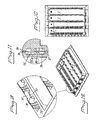
- Fig. 1 a perspective view is shown of those parts of an apparatus casing or apparatus box intended to accommodate electronic components which are required for availability from the exterior of insertable or expansion boards connected to connectors inside the box.
- an apparatus casing for for example a computer, i.e. for a computer box
- Such availability from the exterior is required for a multitude of types of insertable boards such as graphic boards, audio boards, network boards.
- insertable boards such as graphic boards, audio boards, network boards.
- These boards include connectors for exterior connection which can be mounted in a back plate or shielding plate of the board or be available through an opening in the back plate.
- a large rectangular opening 3 is provided, located usually at the back side of the box.
- a plurality of frame parts 5 are attached.
- the back plates 7 can be designed according to a standard.
- the back plates 7 are made from strip-shaped material and have a uniform width but their lower ends are narrower forming bottom tongues 21 intended to be inserted in slots 22 at the rear end bottom of the frame parts 5 for fixing the lower portions of the back plates, see Fig. 3 .
- An intermediate frame part 5 comprises a relatively narrow main portion or upright 23 that extends vertically and at its back side, facing or engaged with edges of the main portions of back plates 7 located at the sides of each other, has a longitudinal groove 25, see Figs. 5 and 1 , for mounting electrically conducting, elastic contact elements designed as back plate contact strips 27. They have as will be described hereinafter, a plurality of contact tongues, the number of which can be adapted to the required contact points, considering for example the wavelengths against which the apparatus casing is intended to shield. Furthermore, the intermediate frame parts 5 have upper and lower portions 29, 31 extending from the interior of the box up to the opening 3.
- the upper and lower portions 29, 31 include vertical tongues 33, 35 extending upwards and downwards respectively and having holes 37, 39 in which screws can engage for attaching the frame part to the plate housing 1.
- the outermost portions 41, 43 of the tongues 33, 35 are thinner than the interior portions and carry upper and lower side contact strips 45 or one or more contact springs 85, see Fig. 14.
- the upper and lower portions 29, 31 also include horizontal portions 47, 49 extending from the narrow vertical main portions 23 to one side thereof, to the same direction where the side frame part 5" that does not provide any opening is located.
- the horizontal portions 47, 49 have a substantially rectangular shape, where the connection to the vertical portions 23 is located at a corner of the rectangular shape.
- the horizontal portion 47 of the upper portion 29 has a hole for cooperation with the screw 9 for securing a back plate 7.
- the horizontal portion 49 of the lower portion 31 is prolonged somewhat backwards, towards the interior of the box, forming a projection 51, see Fig. 5 , in which the slot 22 for fixing the lower edge of the back plate 7 is made.
- This horizontal portion 49 also carries at its rear edge located at the center of the box a vertically extending rectangular tongue 53 located in parallel to the backside of the box and to the corresponding back plate 7.
- This tongue 53 is visible from the outside of the box, also in the case where a back plate 7 is mounted in the frame part 5 and it has a groove or hole 55.
- the groove or hole 55 can be used for attaching signs or labels 57 to the tongues 53 by a suitable cooperating snapping device or possibly a screw.
- the horizontal portions 47, 49 carry at there rear edges located at a distance of the center of the box 3 the upwards and downwards extending tongues 33, 35 respectively for attachment to the apparatus casing 1.
- a thin edge can be provided at the horizontal portions 47, 49 at the side of the place from which these tongues 33, 35 extend, and the widths of this edge can correspond to or preferably somewhat exceed the thickness of the material of the housing 1.
- the vertical main portion 23 can further have a gradual continuation to the horizontal portions of the upper and lower portions by vertical continuation portions 59, 61 which in the embodiment shown have the shapes of rectangular triangles with one small side connecting to an edge of the corresponding horizontal portion and with another small side connecting to the backwards directed side of main portion 23.
- the side frame part 5' that gives an opening for a back plate 7, the left frame part in Fig. 1 is substantially designed as the intermediate frame parts 5 except the fact that the vertical main part 23' thereof carries a vertical thin side plate 63 extending up to the outer side of the frame part and the back side of the box, and the fact that the thin side plate 63 carries a flange part 65 that is located in the same plane as the upwards and downwards directed, respectively, tongues 33', 35' of the upper and lower portions 29', 31' of the frame part and extends away from the opening for the associated back plate 7.
- the side frame part 5' thereby obtains a continuous flange along its upper, left and lower sides and also a continuous narrow edge extending backwards.
- the flange portion 65 carries a side contact strip 45' similar to the side contact strip 45 but having an adapted length or alternatively one or more separate contact springs 85, see Fig. 14.
- the other side frame part 5", the right frame part in Fig. 1 has a vertical main portion 23" like the intermediate frame parts 5 that smoothly, for example such as is shown through triangular portions, connect to the upper and lower portions.
- a thin side plate 63" extends as for the other side frame part 5' to the backside of the box and likewise carries a flange portion.
- the upper and lower portions are here constituted of substantially the uppermost and lowermost portions respectively of the triangular shaped portions (59, 61) and they carry tongues that are directed upwards and downwards respectively so that a connected flange is obtained directed away from the openings for the back plates 7.
- the flange portion also carries a side contact strip 45" designed as the side contact strip 45' or one or more contact springs 85, see Fig. 14.
- Pins 67 cooperate with blind holes 69 in the upper and lower portions of the frame parts 5, 5', 5" in order to give the frame parts accurately defined positions in relation to each other and to give them a good electric connection with each other.
- Fig. 2 frame parts are illustrated mounted to each other for an opening in the housing 1 that is intended for four insertable boards and hence for four back plates 7.
- Three intermediate frame parts 5 and one left side frame part 5' and one right side frame part 5" are required.
- the upper and lower side contact strips 45 have such a length that they extend along the upper and lower tongues of the frame parts when they are mounted to each other.
- the same frame parts are shown as seen from the interior of the box in Fig. 3 whereas cross sectional views are illustrated in Figs. 4 and 5 . In the latter figures is visible how the back plate contact strips 27 are mounted in the grooves 25 in the vertical main portions 23, 23', 23" of the frame parts 5, 5', 5".
- the back plate contact strips are well attached in the grooves and thereby obtain a good electric contact with the material of the main portions 23, 23', 23" of the frame parts and furthermore portions or more particularly tongues of the back plate contact strips elastically press against edges of back plates 7 that are located at the sides of each other, this giving a good electrical connection between the back plates mutually and between the back plates and the frame parts.
- the elastic force from the portions of the back plate contact strips 27 against the back plates have substantially directions parallel to the large surfaces of the main portions 19 of the back plates, i.e. they pass in the plane of these main portions. This is advantageous since the back plates cannot themselves move elastically in this direction and hence appear as totally stiff in relation to the back plate contact strips 27.
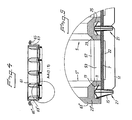
- a back plate contact strip 27 in a non-tensioned state is shown in Figs. 6 and 7 respectively.
- the back plate contact strips 27 are like the side contact strips 45, 45', 45" made from a strip of elastic, electrically conducting material. Suitable portions of the strip have been removed by punching and then or in connection with the punching the remaining part has been bent.
- a back plate contact strip 27 in this embodiment comprises a substantially whole, flat strip shaped main portion or web portion 71 from the two opposite edges of which tongues or flaps extend that are bent alternatingly to opposite sides.
- the flaps 73 that are intended for contacting the edge surfaces of the back plates extend from the inner edge of the main portion 71 and have a rectangular shape and a length corresponding to approximately the width of the main portion. They can have a weak bending along their center lines extending perpendicularly to the longitudinal axis of the main portion in order to facilitate insertion of the back plate contact strip and to give a good point contact with edge surfaces of the back plates 7.
- the flaps 73 are further, at their connection to the main portion 71, bent so that they form a relatively small angle of about 15 - 30° to the main portion.
- Rectangular, shorter tongues or flaps 75 extend from the opposite, exterior edge of the main portion 71 and have substantially the same width as that of the inner flaps 75 but are shorter and have a length which for example can correspond to approximately half the width of the main portion 71.
- Each exterior flap 75 is located opposite an inner flap 73 that is bent to the opposite direction.
- the outer flaps 75 are at their connection to the main portion 71 bent so that they form a relatively large angle to the main portion, say about 60 - 80°, and press with their outer free edge, when the back plate contact strip is mounted, against the opposite side walls in the groove 25 and thereby keep the contact strip in place.
- the outer flaps 75 are totally inserted in the grooves, see Fig. 5 .
- the outer edge surface of the main portion 71 is engaged with the bottom of the grooves and the outer flaps elastically press against the side walls of the grooves and can even somewhat penetrate therein if the material of the frame parts is relatively soft. More than half the width of the main portion 71 is located outside the grooves whereas the outermost portions of the inner flaps 73 are located inside the grooves and are engaged with the side walls thereof as long as no back plate 7 is mounted. Due to the bending of the inner flaps 73 in their longitudinal direction they are with point contacts engaged with the side walls.
- the back plate contact strips 27 are mounted in the grooves 25 using a tool, not shown, so that the outer flaps 75 are pressed down into the grooves and act as barbs and thereby keep the contact strips in the grooves.
- the contact flaps 73 are bent inwards towards the web of the contact strips so far that they become located inside the walls of the groove 27.
- the contact flaps 73 move elastically towards the walls of the groove 25 after releasing the tool.
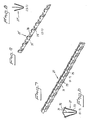
- FIG. 8 An alternative embodiment 27' of the back plate contact strips appears from the cross sectional view of Fig. 8 and the perspective view of Fig. 9 .
- the main portion 71' has as in the first embodiment a flat configuration of substantially a strip-shape, including only inner bent flaps 73', designed and bent in the same ways as the flaps 73 in the first embodiment whereas at the opposite outer edge, relatively short tongues 76 extend, these tongues thus located in the same plane as the main portion.
- Wider recesses 77 are thus provided for the inner bent flaps 73' and narrower recesses 78 for the tongues 76 which, using an adapted tool, not shown, are pressed into them, so that the edges of the tongues cut into the end surfaces of the recesses 78, whereby a good mechanical attachment and a good electrical contacting is obtained.
- shorter recesses 79 are provided so that at the connection between two inner flaps 73' short projections 80 extending laterally are obtained that are engaged with the web portion 71'.
- the contact between the inner flaps 73' and the back plates 7 is obtained in the same way as for the first embodiment.
- the tongues 76 additionally keep, when they are inserted in the recesses 78, the web portion 71' in a straight state.
- the different elastic contact strips and contact elements of elastic plate material that have been described above can in some cases advantageously be replaced by elastic elements, not shown, made from a body of a material having some or a considerable elasticity, for example from an elastomer or a rubber material.
- the elastic body is coated with a surface layer of electrically conducting material such as a suitable metal which can have been attached using for example sputtering.
- Back plate contact strips made in this way can for example have a cross section having an outer profile approximately agreeing with the outer profile of the back plate contact strips 27, 27', see Figs. 6 and 8 , having oblique large surfaces for contact with back plates and can be attached by an adhesive in suitable grooves or recesses, compare the recesses 25 in Fig. 5 .
- Back plate contact strips can thus have contact surfaces to the back plates that are located in a relatively small angle in relation to each other, i.e. in the range of 5 - 30°.
- the contact surfaces can also be substantially parallel.
- the advantage of elastic strips of this kind is that an electrical contacting can be obtained along the whole length of the strips which can improve the shielding against high frequency electromagnetic fields.
Landscapes
- Engineering & Computer Science (AREA)
- Theoretical Computer Science (AREA)
- General Engineering & Computer Science (AREA)
- Computer Hardware Design (AREA)
- General Physics & Mathematics (AREA)
- Physics & Mathematics (AREA)
- Human Computer Interaction (AREA)
- Power Engineering (AREA)
- Microelectronics & Electronic Packaging (AREA)
- Shielding Devices Or Components To Electric Or Magnetic Fields (AREA)
- Mounting Of Printed Circuit Boards And The Like (AREA)
- Connector Housings Or Holding Contact Members (AREA)
- Coupling Device And Connection With Printed Circuit (AREA)
- Multi-Conductor Connections (AREA)
Applications Claiming Priority (3)
| Application Number | Priority Date | Filing Date | Title |
|---|---|---|---|
| SE0102322A SE523388C2 (sv) | 2001-06-27 | 2001-06-27 | Hölje för elektroniska anordningar med en öppning för instickskort samt kontaktelement för elektrisk förbindning mellan en panel för instickskort och ett apparathölje |
| SE0102322 | 2001-06-27 | ||
| PCT/SE2002/001292 WO2003003802A1 (en) | 2001-06-27 | 2002-06-27 | Housing for electronic circuits, electrically connecting element and contact spring, procedure for electromagnetic shielding |
Publications (2)
| Publication Number | Publication Date |
|---|---|
| EP1407645A1 EP1407645A1 (en) | 2004-04-14 |
| EP1407645B1 true EP1407645B1 (en) | 2010-11-03 |
Family
ID=20284671
Family Applications (1)
| Application Number | Title | Priority Date | Filing Date |
|---|---|---|---|
| EP02744059A Expired - Lifetime EP1407645B1 (en) | 2001-06-27 | 2002-06-27 | Electrically connecting element between a back plate and another back plate or a housing for electronic circuits |
Country Status (9)
Families Citing this family (16)
| Publication number | Priority date | Publication date | Assignee | Title |
|---|---|---|---|---|
| JP2005251309A (ja) * | 2004-03-04 | 2005-09-15 | Hitachi Ltd | ディスクアレイ装置 |
| JP4672599B2 (ja) * | 2006-05-26 | 2011-04-20 | 富士通テレコムネットワークス株式会社 | プラグインユニット板の表示構造 |
| SE534234C2 (sv) * | 2009-10-23 | 2011-06-07 | Clamco Invest Ab | Hölje för elektronisk utrustning |
| SE0950788A1 (sv) * | 2009-10-23 | 2010-10-05 | Clamco Invest Ab | Hölje för elektronisk utrustning, innefattande kontakteringsanordning |
| US8270929B1 (en) * | 2011-09-09 | 2012-09-18 | Contech RF Devices, LLC | RF shielding for mobile devices |
| EP3118715B1 (en) * | 2013-02-28 | 2023-07-26 | Oracle International Corporation | Electrical interconnection of rack-mounted field replaceable units |
| CN104122961A (zh) * | 2013-04-25 | 2014-10-29 | 鸿富锦精密工业(深圳)有限公司 | 机柜式服务器及虚拟服务器机箱 |
| GB2522806B (en) | 2013-06-14 | 2016-01-06 | Eschmann Holdings Ltd | Surgical table and method of operating the same |
| CN104238656A (zh) * | 2013-06-24 | 2014-12-24 | 鸿富锦精密工业(深圳)有限公司 | 扩充卡固定装置 |
| GB2516051B (en) | 2013-07-09 | 2016-06-08 | Eschmann Holdings Ltd | Surgical tables |
| GB2535054B (en) | 2013-07-12 | 2017-01-11 | Eschmann Holdings Ltd | Tabletop sections for surgical tables |
| CN105241293B (zh) * | 2015-10-30 | 2017-05-31 | 成都标建铝业有限公司 | 一种增强散热效果的散热器型材 |
| CN106647444B (zh) * | 2016-10-31 | 2023-08-01 | 国网山东省电力公司莱芜供电公司 | 采用负反馈的电源调节装置及其调节方法 |
| CN109358715B (zh) * | 2018-10-26 | 2021-10-01 | 英业达科技有限公司 | 计算机机壳 |
| BE1026757B1 (de) * | 2018-11-07 | 2020-06-08 | Phoenix Contact Gmbh & Co | Baugruppe eines Elektronikgeräts mit einem Gerätegehäuse und einer Elektronikbaugruppe |
| CN112462862B (zh) * | 2019-09-06 | 2023-04-07 | 英业达科技有限公司 | 用于扩充卡槽口的电磁遮蔽结构及其扩充卡挡板 |
Family Cites Families (11)
| Publication number | Priority date | Publication date | Assignee | Title |
|---|---|---|---|---|
| DE3907412A1 (de) | 1989-03-08 | 1990-09-13 | Ant Nachrichtentech | Gehaeusesystem zur aufnahme von elektrischen einschueben |
| JP3011379B2 (ja) * | 1991-07-17 | 2000-02-21 | 北川工業株式会社 | 電磁波シールド用ガスケット |
| IT1255012B (it) * | 1992-03-27 | 1995-10-13 | Italtel Spa | Dispositivo di schermatura elettromagnetica |
| US5957465A (en) * | 1997-06-17 | 1999-09-28 | Sun Microsystems, Inc. | Modular EMC PCI card gasket |
| US5929376A (en) * | 1997-06-20 | 1999-07-27 | Tektronix, Inc. | Electromagnetic interference shield and method of manufacturing |
| US5952608A (en) * | 1997-08-11 | 1999-09-14 | Kim; Sun-Ki | Finger strip for shielding electromagnetic wave and front panel assembly mounting the same |
| US6201711B1 (en) * | 1999-05-18 | 2001-03-13 | Hewlett-Packard Company | Computer system housing for attenuating electromagnetic inferference (EMI) |
| US6332618B1 (en) * | 1999-09-20 | 2001-12-25 | Telefonaktiebolaget Lm Ericsson (Publ) | Double sided gasket |
| US6403879B1 (en) * | 2000-06-21 | 2002-06-11 | Hewlett-Packard Company | Electronic chassis having an EMI gasket and integral ventilation holes |
| WO2002037920A1 (en) | 2000-11-03 | 2002-05-10 | Instrument Specialities Company, Inc. | Modular shielding of openings with passing cables |
| US6618271B1 (en) * | 2002-04-01 | 2003-09-09 | Gateway, Inc. | EMI shield |
-
2001
- 2001-06-27 SE SE0102322A patent/SE523388C2/sv not_active IP Right Cessation
-
2002
- 2002-06-27 WO PCT/SE2002/001292 patent/WO2003003802A1/en active Application Filing
- 2002-06-27 AT AT02744059T patent/ATE487360T1/de not_active IP Right Cessation
- 2002-06-27 DE DE60238197T patent/DE60238197D1/de not_active Expired - Lifetime
- 2002-06-27 CN CNB028166566A patent/CN1331378C/zh not_active Expired - Fee Related
- 2002-06-27 KR KR10-2003-7017055A patent/KR20040038920A/ko not_active Ceased
- 2002-06-27 US US10/481,589 patent/US7158388B2/en not_active Expired - Fee Related
- 2002-06-27 EP EP02744059A patent/EP1407645B1/en not_active Expired - Lifetime
- 2002-06-27 JP JP2003509832A patent/JP4126013B2/ja not_active Expired - Fee Related
Also Published As
| Publication number | Publication date |
|---|---|
| EP1407645A1 (en) | 2004-04-14 |
| US20040196627A1 (en) | 2004-10-07 |
| CN1331378C (zh) | 2007-08-08 |
| SE0102322D0 (sv) | 2001-06-27 |
| DE60238197D1 (de) | 2010-12-16 |
| SE0102322L (sv) | 2002-12-28 |
| JP2004531095A (ja) | 2004-10-07 |
| WO2003003802A1 (en) | 2003-01-09 |
| SE523388C2 (sv) | 2004-04-13 |
| US7158388B2 (en) | 2007-01-02 |
| CN1547876A (zh) | 2004-11-17 |
| JP4126013B2 (ja) | 2008-07-30 |
| KR20040038920A (ko) | 2004-05-08 |
| ATE487360T1 (de) | 2010-11-15 |
Similar Documents
| Publication | Publication Date | Title |
|---|---|---|
| EP1407645B1 (en) | Electrically connecting element between a back plate and another back plate or a housing for electronic circuits | |
| JP2927564B2 (ja) | モジュラージャック装置用2部分ソケットユニット | |
| US7497717B2 (en) | Land grid array connector having improved cover | |
| US7714237B2 (en) | Electrical apparatus and supporting frame for wall-mounting same | |
| JP2625546B2 (ja) | 機器のカバーのための取付装置 | |
| JP6498409B2 (ja) | コネクタ組立体 | |
| EP0762324A2 (en) | PC card socket connector and PC card with same | |
| US7443666B2 (en) | Mounting apparatus for mounting expansion cards in computer enclosure | |
| US6356321B1 (en) | Liquid crystal display panel holder | |
| US7226311B2 (en) | Socket assembly for card | |
| US6267254B1 (en) | Mother board tray assembly | |
| JP2009181799A (ja) | カードコネクタ | |
| US6979211B1 (en) | Expansion device with a masking bracket for a card bus connector | |
| EP0210686A2 (en) | Electrical connector with mounting members | |
| US6131274A (en) | Apparatus and method for guiding a circuit board into an electronic chassis | |
| CN212516983U (zh) | 一种触控开关的通用底座及具有通用底座的触控开关 | |
| JPH0327411A (ja) | パーソナルコンピュータ | |
| KR19990044605A (ko) | 메모리 카드 커넥터 | |
| JP4715583B2 (ja) | 電子機器ユニットのシールド構造 | |
| CN114464217B (zh) | 扣合装置 | |
| JPH0745993Y2 (ja) | プリント板ユニットにおける前面シールド板の構造 | |
| EP0752809A1 (en) | Enclosure for a printed circuit board | |
| JP2539712Y2 (ja) | 電気装置筐体 | |
| CN100468145C (zh) | 液晶显示装置 | |
| CN2557997Y (zh) | 磁架卡合结构 |
Legal Events
| Date | Code | Title | Description |
|---|---|---|---|
| PUAI | Public reference made under article 153(3) epc to a published international application that has entered the european phase |
Free format text: ORIGINAL CODE: 0009012 |
|
| 17P | Request for examination filed |
Effective date: 20040112 |
|
| AK | Designated contracting states |
Kind code of ref document: A1 Designated state(s): AT BE CH CY DE DK ES FI FR GB GR IE IT LI LU MC NL PT SE TR |
|
| AX | Request for extension of the european patent |
Extension state: AL LT LV MK RO SI |
|
| 17Q | First examination report despatched |
Effective date: 20090918 |
|
| GRAP | Despatch of communication of intention to grant a patent |
Free format text: ORIGINAL CODE: EPIDOSNIGR1 |
|
| RTI1 | Title (correction) |
Free format text: ELECTRICALLY CONNECTING ELEMENT BETWEEN A BACK PLATE AND ANOTHER BACK PLATE OR A HOUSING FOR ELECTRONIC CIRCUITS |
|
| RIC1 | Information provided on ipc code assigned before grant |
Ipc: H05K 9/00 20060101ALI20100506BHEP Ipc: H05K 5/00 20060101AFI20100506BHEP |
|
| RTI1 | Title (correction) |
Free format text: ELECTRICALLY CONNECTING ELEMENT BETWEEN A BACK PLATE AND ANOTHER BACK PLATE OR A HOUSING FOR ELECTRONIC CIRCUITS |
|
| GRAS | Grant fee paid |
Free format text: ORIGINAL CODE: EPIDOSNIGR3 |
|
| GRAA | (expected) grant |
Free format text: ORIGINAL CODE: 0009210 |
|
| AK | Designated contracting states |
Kind code of ref document: B1 Designated state(s): AT BE CH CY DE DK ES FI FR GB GR IE IT LI LU MC NL PT SE TR |
|
| REG | Reference to a national code |
Ref country code: GB Ref legal event code: FG4D |
|
| REG | Reference to a national code |
Ref country code: CH Ref legal event code: EP |
|
| REG | Reference to a national code |
Ref country code: IE Ref legal event code: FG4D |
|
| REF | Corresponds to: |
Ref document number: 60238197 Country of ref document: DE Date of ref document: 20101216 Kind code of ref document: P |
|
| REG | Reference to a national code |
Ref country code: NL Ref legal event code: VDEP Effective date: 20101103 |
|
| PG25 | Lapsed in a contracting state [announced via postgrant information from national office to epo] |
Ref country code: NL Free format text: LAPSE BECAUSE OF FAILURE TO SUBMIT A TRANSLATION OF THE DESCRIPTION OR TO PAY THE FEE WITHIN THE PRESCRIBED TIME-LIMIT Effective date: 20101103 Ref country code: PT Free format text: LAPSE BECAUSE OF FAILURE TO SUBMIT A TRANSLATION OF THE DESCRIPTION OR TO PAY THE FEE WITHIN THE PRESCRIBED TIME-LIMIT Effective date: 20110303 Ref country code: SE Free format text: LAPSE BECAUSE OF FAILURE TO SUBMIT A TRANSLATION OF THE DESCRIPTION OR TO PAY THE FEE WITHIN THE PRESCRIBED TIME-LIMIT Effective date: 20101103 Ref country code: AT Free format text: LAPSE BECAUSE OF FAILURE TO SUBMIT A TRANSLATION OF THE DESCRIPTION OR TO PAY THE FEE WITHIN THE PRESCRIBED TIME-LIMIT Effective date: 20101103 Ref country code: FI Free format text: LAPSE BECAUSE OF FAILURE TO SUBMIT A TRANSLATION OF THE DESCRIPTION OR TO PAY THE FEE WITHIN THE PRESCRIBED TIME-LIMIT Effective date: 20101103 |
|
| PG25 | Lapsed in a contracting state [announced via postgrant information from national office to epo] |
Ref country code: GR Free format text: LAPSE BECAUSE OF FAILURE TO SUBMIT A TRANSLATION OF THE DESCRIPTION OR TO PAY THE FEE WITHIN THE PRESCRIBED TIME-LIMIT Effective date: 20110204 |
|
| PG25 | Lapsed in a contracting state [announced via postgrant information from national office to epo] |
Ref country code: BE Free format text: LAPSE BECAUSE OF FAILURE TO SUBMIT A TRANSLATION OF THE DESCRIPTION OR TO PAY THE FEE WITHIN THE PRESCRIBED TIME-LIMIT Effective date: 20101103 Ref country code: ES Free format text: LAPSE BECAUSE OF FAILURE TO SUBMIT A TRANSLATION OF THE DESCRIPTION OR TO PAY THE FEE WITHIN THE PRESCRIBED TIME-LIMIT Effective date: 20110214 |
|
| PG25 | Lapsed in a contracting state [announced via postgrant information from national office to epo] |
Ref country code: DK Free format text: LAPSE BECAUSE OF FAILURE TO SUBMIT A TRANSLATION OF THE DESCRIPTION OR TO PAY THE FEE WITHIN THE PRESCRIBED TIME-LIMIT Effective date: 20101103 |
|
| PLBE | No opposition filed within time limit |
Free format text: ORIGINAL CODE: 0009261 |
|
| STAA | Information on the status of an ep patent application or granted ep patent |
Free format text: STATUS: NO OPPOSITION FILED WITHIN TIME LIMIT |
|
| 26N | No opposition filed |
Effective date: 20110804 |
|
| REG | Reference to a national code |
Ref country code: DE Ref legal event code: R097 Ref document number: 60238197 Country of ref document: DE Effective date: 20110804 |
|
| PG25 | Lapsed in a contracting state [announced via postgrant information from national office to epo] |
Ref country code: IT Free format text: LAPSE BECAUSE OF FAILURE TO SUBMIT A TRANSLATION OF THE DESCRIPTION OR TO PAY THE FEE WITHIN THE PRESCRIBED TIME-LIMIT Effective date: 20101103 |
|
| REG | Reference to a national code |
Ref country code: CH Ref legal event code: PL |
|
| REG | Reference to a national code |
Ref country code: IE Ref legal event code: MM4A |
|
| PG25 | Lapsed in a contracting state [announced via postgrant information from national office to epo] |
Ref country code: LI Free format text: LAPSE BECAUSE OF NON-PAYMENT OF DUE FEES Effective date: 20110630 Ref country code: IE Free format text: LAPSE BECAUSE OF NON-PAYMENT OF DUE FEES Effective date: 20110627 Ref country code: CH Free format text: LAPSE BECAUSE OF NON-PAYMENT OF DUE FEES Effective date: 20110630 |
|
| PG25 | Lapsed in a contracting state [announced via postgrant information from national office to epo] |
Ref country code: MC Free format text: LAPSE BECAUSE OF NON-PAYMENT OF DUE FEES Effective date: 20110630 |
|
| PG25 | Lapsed in a contracting state [announced via postgrant information from national office to epo] |
Ref country code: CY Free format text: LAPSE BECAUSE OF FAILURE TO SUBMIT A TRANSLATION OF THE DESCRIPTION OR TO PAY THE FEE WITHIN THE PRESCRIBED TIME-LIMIT Effective date: 20101103 Ref country code: LU Free format text: LAPSE BECAUSE OF NON-PAYMENT OF DUE FEES Effective date: 20110627 |
|
| PG25 | Lapsed in a contracting state [announced via postgrant information from national office to epo] |
Ref country code: TR Free format text: LAPSE BECAUSE OF FAILURE TO SUBMIT A TRANSLATION OF THE DESCRIPTION OR TO PAY THE FEE WITHIN THE PRESCRIBED TIME-LIMIT Effective date: 20101103 |
|
| PGFP | Annual fee paid to national office [announced via postgrant information from national office to epo] |
Ref country code: FR Payment date: 20130716 Year of fee payment: 12 |
|
| PGFP | Annual fee paid to national office [announced via postgrant information from national office to epo] |
Ref country code: GB Payment date: 20131219 Year of fee payment: 12 |
|
| PGFP | Annual fee paid to national office [announced via postgrant information from national office to epo] |
Ref country code: DE Payment date: 20141230 Year of fee payment: 13 |
|
| GBPC | Gb: european patent ceased through non-payment of renewal fee |
Effective date: 20140627 |
|
| REG | Reference to a national code |
Ref country code: FR Ref legal event code: ST Effective date: 20150227 |
|
| PG25 | Lapsed in a contracting state [announced via postgrant information from national office to epo] |
Ref country code: FR Free format text: LAPSE BECAUSE OF NON-PAYMENT OF DUE FEES Effective date: 20140630 Ref country code: GB Free format text: LAPSE BECAUSE OF NON-PAYMENT OF DUE FEES Effective date: 20140627 |
|
| REG | Reference to a national code |
Ref country code: DE Ref legal event code: R119 Ref document number: 60238197 Country of ref document: DE |
|
| PG25 | Lapsed in a contracting state [announced via postgrant information from national office to epo] |
Ref country code: DE Free format text: LAPSE BECAUSE OF NON-PAYMENT OF DUE FEES Effective date: 20160101 |