EP1406087B1 - Schaltung zur Spannungsbegrenzung an den Elektroden in einer CHEF Pulselektrophoresekammer - Google Patents
Schaltung zur Spannungsbegrenzung an den Elektroden in einer CHEF Pulselektrophoresekammer Download PDFInfo
- Publication number
- EP1406087B1 EP1406087B1 EP02740214.8A EP02740214A EP1406087B1 EP 1406087 B1 EP1406087 B1 EP 1406087B1 EP 02740214 A EP02740214 A EP 02740214A EP 1406087 B1 EP1406087 B1 EP 1406087B1
- Authority
- EP
- European Patent Office
- Prior art keywords
- electrodes
- diodes
- circuit
- power supply
- voltage
- Prior art date
- Legal status (The legal status is an assumption and is not a legal conclusion. Google has not performed a legal analysis and makes no representation as to the accuracy of the status listed.)
- Expired - Lifetime
Links
Images




Classifications
-
- G—PHYSICS
- G01—MEASURING; TESTING
- G01N—INVESTIGATING OR ANALYSING MATERIALS BY DETERMINING THEIR CHEMICAL OR PHYSICAL PROPERTIES
- G01N27/00—Investigating or analysing materials by the use of electric, electrochemical, or magnetic means
- G01N27/26—Investigating or analysing materials by the use of electric, electrochemical, or magnetic means by investigating electrochemical variables; by using electrolysis or electrophoresis
- G01N27/416—Systems
- G01N27/447—Systems using electrophoresis
- G01N27/44704—Details; Accessories
- G01N27/44713—Particularly adapted electric power supply
-
- G—PHYSICS
- G01—MEASURING; TESTING
- G01N—INVESTIGATING OR ANALYSING MATERIALS BY DETERMINING THEIR CHEMICAL OR PHYSICAL PROPERTIES
- G01N27/00—Investigating or analysing materials by the use of electric, electrochemical, or magnetic means
- G01N27/26—Investigating or analysing materials by the use of electric, electrochemical, or magnetic means by investigating electrochemical variables; by using electrolysis or electrophoresis
- G01N27/416—Systems
- G01N27/447—Systems using electrophoresis
- G01N27/44756—Apparatus specially adapted therefor
- G01N27/44773—Multi-stage electrophoresis, e.g. two-dimensional electrophoresis
Definitions
- the present invention is related to electric equipments used in electrophoresis, specifically to the generation of contour clamped electric potentials for generating homogeneous fields which alternate its direction of application.
- the electrophoresis is a technique which separates molecules by their differential migration inside an electric field.
- the molecules can be placed in a gel and they are sieved when the electric field that compels them to migrate is applied.
- the negative charged molecules migrate toward the anode and the positive charged ones make it toward the cathode. This way the molecules are separated in bands inside the gel, according to their size.
- Two parallel electrodes are usually disposed for the generation of the electric field; they are connected to the positive and negative outputs of a power supply.
- DNA molecules are negatively charged when they are dissolved in buffer at neuter or alkaline pH. When the electric field is applied, DNA molecules are elongated and their charge-mass ratio becomes independent of its molecular size.
- Pulsed field gel electrophoresis was created by Schwartz and Cantor in 1984 (Cell, 37, pp 67-75, 1984 ; US Patent 4,473,452 of September 25th, 1984 ) and it increased the range of the DNA molecules that could be separated in electrophoresis.
- the authors obtained that the large intact DNA molecules, larger than 20000 base pairs, were separated in band patterns inside agarose gels by means of the application of electric pulses of selected duration that periodically alternated their direction of application regarding the separation gel.
- the changes in the direction of the electric field application cause reorientation of the DNA molecules migration, while the duration of this reorientation depends on the molecular size.
- the resulting band patterns have been denominated 'electrophoretic patterns', 'molecular kariotypes', 'electrophoretic kariotypes', etc.
- any system of pulsed field gel electrophoresis consists of:
- One of the methods to clamp the potential values in the CHEF electrodes is to use a network of resistors that are connected in series. This network forms a voltage divider among the values zero and 'V 0 '. We will name nodes to the place of union between two serial resistors of the voltage divider and at each node is connected an electrode of the hexagon.
- the potential difference is applied to other two different groups of electrodes. This is carried out with relays and diodes which connect the electrodes that should be polarized with zero volt and 'Vo' to the outputs of the power supply through the system for the electric fields switching.
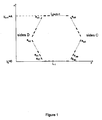
- L 1 side is defined arbitrarily and it is placed on the 'X' axis of a Cartesian plane.
- the opposed side (denominated as L (m/2)+1 ) is located at a distance 'A' from the 'X' axis. This way, the remaining sides of the regular polygon are symmetrically distributed to both sides of the L 1 and L (m/2)+1 sides. Those sides of the regular polygon that are to the left of the sides L 1 and L (m/2)+1 will be denominated as sides 'C' and those that are to the right like sides 'D'.
- the two E iC and E iD electrodes are placed at the same distance y i of the 'X' axis, where 'i' is a natural number between 1 and 'n'. Each one of those ([E 1C -E 1D ], [E 2C -E 2D ],.., [E nC -E nD ]) will be denominated P i electrode pairs.
- An embodiment of a device for gel electrophoresis using contour-clamped electric field is known from EP 0 356 187 .
- a close network of resistors is provided wherein a transistorized buffer circuit is employed for each electrode.
- An embodiment of a contour-clamped homogeneous electric field generator is known from EP 0 342 349 .
- a circuit with operational amplifiers and MOSFETs is provided.
- the electrodes of the closed contour are polarized for generating a homogeneous electric field in a determined direction of application.
- a similar reasoning is applicable to achieve a homogeneous electric field of same magnitude, but whose lines of force have another direction. It is only necessary to define another side of the regular polygon as L 1 .
- both electric fields of the PFGE can be energized with two identical clamping circuits.
- the clamping circuits are connected between the positive and negative outputs of the power supply by means of another circuit or alternator which alternates the electric fields in a way that only one clamping circuits receives electric energy each time.
- Each clamping circuit imposes in the electrodes the voltages which generate an electric field of homogeneous intensity in one application direction inside the CHEF chamber.
- the corresponding circuit is connected as follows:
- the voltage repeaters are of two types:
- each R i resister is chosen to guarantee that the voltage at each P i electrode pair was proportional to the distance that separates them from the electrodes located on the L 1 side of the regular polygon.
- the other circuit is identical to this, but it is connected to the Ei electrodes in a different way.
- another side of the polygon is redefined as L 1 side and the reference system is rotated the necessary angle in order to the new L 1 side was at the 'X' axis.
- the 'C' and 'D' sides, the Ei electrodes and the P i electrode pairs are redefined starting from the L 1 side.
- the influence of the buffer changes of conductivity upon the potential of each N i node of the divider is decreased by sourcing current into or sinking current away from the electrode until its voltage equals its node voltage.
- Transistors in "emitter follower" configuration are used as current sources.
- the electrode pairs located nearer the negative output should always extract current from the buffer because their potentials tend to be higher than the one at its corresponding reference node. For this reason a PNP type transistors is used which sink this current toward the negative output of the power supply.
- the electrode pairs located nearer the positive output should always source current into the buffer because their potential tend to be lower than the one at its corresponding node.
- a NPN type transistor is used which gets current from the positive output. In that way the potential of the reference nodes it is not considerably affected.
- Each electrode pair potential resembles to its reference potential but it differs in a certain value. The difference is caused by the transistor base to emitter and diode voltage drops associated to the electrode pairs. This voltage drop is characteristic of the PN junctions of the silicon semiconductor elements and it is approximately similar to 0,7 volt.
- the change in the transistors and diodes polarity that occurs in the center of the divider introduces an error in the voltage applied to the electrodes.
- This error can be compensated by inserting diodes in series with the central resister of the voltage divider. This way the potential of the reference nodes is modified in the same magnitude but in opposite sense to the effect of the voltage drops in the transistors and diodes of each pair.
- the circuit proposed in this invention consists of two identical parts that are connected to the power supply through another appropriate electronic circuit to alternate the electric fields with the wanted intensity and pulse duration.
- Example 1 Circuit to polarize the electrodes of a hexagonal chamber of 18 electrodes.
- a group of electrodes 101 to 118 placed on a regular hexagon at three electrodes per each side is shown.
- the electrodes 101, 102 and 103 are polarized with the maximum potential, close to the potential of the power supply's positive output.
- the electrodes 110, 111 and 112 are polarized with the minimum potential, close to 0 volts.
- the rest of the electrodes are organized in pairs (table I). Each electrode from the same pair will be polarized with the same voltage, the one proportional to the distance from each pair to the electrodes of the A- group.
- the electrodes 113, 114 and 115 are polarized with the maximum potential, close to the potential of the power supply's positive output.
- the electrodes 104, 105 and 106 are polarized with the minimum potential, close to 0 volt.
- the rest of the electrodes is organized in pairs (table I). Each electrode from the same pair will be polarized with the same voltage, the one proportional to the distance from each pair to the electrodes of the B- group.
- the lines show the number of the electrodes that should be polarized at the same voltage to generate a homogeneous electric field in the two A and B application directions in a chamber with an electrode disposition similar to one in figure 1 .
- the resistors 201 and 202 connected in series are necessary to generate the reference potentials in this CHEF chamber with three electrodes per side ( figure 3 ).
- the resistors 201 are of the same value, the resistors 202 have the half of this value.
- the ladder of resistors 201 and 202 is connected between the positive (+) and negative (-) outputs of a power supply through switches or the alternator. This voltage divider generates the reference potentials that appear in the nodes 203 and 204.
- the voltage repeaters 205 and 206 take the voltage from the reference nodes 203 and 204 to appropriately polarize the electrodes in A and B directions.
- Voltage repeaters 205 and 206 are detailed shown in figure 4 .
- the base of the NPN type single transistor 301 is connected to the node 203.
- the collector of the single transistor 301 is connected to the positive output (+) through switches.
- the emitter of the single transistor 301 are connected to the anodes of two diodes 302, which in turn are connected by the cathode to the electrodes whose potential corresponds to that particular node 203.
- the base of the PNP type single transistor 303 is connected to the node 204.
- the collector of the single transistor 303 is connected to the negative output (-) through switches.
- the emitter of the single transistor 303 are connected to the cathodes of two diodes 304 which in turn are connected by the anode to the electrodes whose potential corresponds to that particular node 204.
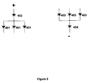
- the electrodes of A+ and B+ groups ( figure 5 ) are connected to the cathode of diodes 401 connected together by their anodes.
- the anode of the diodes 401 is connected to the cathode of another diode 402 which in turn is connected by its anode to the positive output of the power supply through switches.
- the electrodes of A- and B- groups are connected to the anode of diodes 403 connected together by their cathode.
- the cathode of the diodes 403 is connected to the anode of another diode 404 which in turn is connected by its cathode to the positive output of the power supply through switches.
- the diodes 402 and 404 guarantee that the branches which polarize the electrodes of the A+, A-, B+ and B- groups have the same voltage drops provoked by the PN junctions that the rest of the electrodes of the array.
- the diodes 207 ( figure 3 ) compensate the errors caused by the polarity change of the transistors and diodes in the voltage applied to the electrodes.
- the energy was obtained from a 'Macrodrive I' power supply adjusted to a 120,0 volt constant voltage among the positive (+) and negative (-) outputs in the A and B directions.
- Table II Theoretical values and the ones generated by the presented circuit in the electrodes of a CHEF chamber with 18 electrodes located on the sides of a hexagon.
- V Theoretical Voltages (V) Real Voltages (V) A Direction B Direccion 118,6 101, 102 y 103 : 118,7 115, 114 y 113: 118,7 108,8 118: 108,8 104: 108,9 116: 108,8 112: 108,8 89,3 117: 89,2 105: 89,2 117: 89,2 111: 89,2 69,8 116: 69,7 106: 69,7 118: 69,7 110: 69,6 50,2 115: 50,2 107: 50,3 101: 50,4 109: 50,3 30,7 114: 30,8 108: 30,8 102: 30,8 108: 30,8 11,2 113: 11,2 109: 11,2 103: 11,2 107: 11,2 1,4 112, 111 y 110: 1,4 104, 105 y 106: 1,4
- Electrode numbers, according figure 2 are in bold typeface.
- Example 2 Circuit to polarize the punctual electrodes of a hexagonal chamber with 36 electrodes not evenly distributed.
- a group of punctual electrodes 501 to 536 placed upon a regular hexagon at six electrodes per each side is shown.
- the electrodes 501 to 506 (denominated A+ group) are polarized with the maximum potential, close to the potential of the power supply's positive output.
- the electrodes 519 to 524 (denominated A- group) are polarized with the minimum potential, close to 0 volts.
- the rest of the electrodes are organized in pairs (table III). Each electrode from the same pair will be polarized with the same voltage, the one proportional to the distance from each pair to the electrodes of the A- group.
- the electrodes 525 to 530 are polarized with the maximum potential, close to the potential of the power supply's positive output.
- the electrodes 507 to 512 are polarized with the minimum potential, near to 0 volt.
- the rest of the electrodes are organized in pairs (table III). Each electrode from the same pair will be polarized with the same voltage, the one proportional to the distance from each pair to the electrodes of the B- group.
- the distances between two consecutive electrodes are not the same.
- the distance between the electrode 501 and the 502 are different to the distance between the electrode 502 and the electrode 503.
- resistors 601, 602 and 603 To generate the reference potentials in this CHEF chamber with six electrodes per side thirteen resistors 601, 602 and 603 connected in series are needed ( figure 7 ).
- the resistance values of resistors 601, 602 and 603 should be chosen in order to the potential at each electrode be proportional to the distance between each electrode and the electrodes of the A- and B- groups for each one of the A and B directions, respectively.
- the resistors 601 were of 348 ohm
- the resistors 602 are of 470 ohm
- the resistors 603 are of 235 ohm.
- the chain of resistors 601, 602 and 603 are connected to the positive (+) and negative (-) potentials of a power supply through switches.
- This voltage divider generates the reference potentials that appear in the nodes 604 and 605.
- the voltage repeaters 606 and 607 take the voltage from the reference nodes 604 and 605 to properly polarize the electrodes in A and B directions.
- the voltage repeaters 606 and 607 are identical to the repeaters 205 and 206 ( figure 3 ).
- Diodes 608 are inserted in series with the resistors to correct the errors in the voltage applied to the electrodes caused by the polarity change of the active transistors inside the voltage repeaters 606 and 607. Table III. Theoretical values and the one generated by the presented circuit in the electrodes of a CHEF chamber with 36 electrodes placed on the sides of a hexagon.
- V Theoretical voltages
- V Real Voltages
- V A Direction B Direction 118,80 501,502,503,504,505,506 :118,75 525,526,527,528,529,530 :118,75 113,18 536 :113,15 507 :113,15 524 :113,15 531 :113,15 104,85 535 :104,70 508 :104,70 523 :104,75 532 :104,75 93,62 534 :93,40 509 : 93,40 522 :93,40 533 : 93,40 85,28 533 :85,05 510 : 85,05 521 :85,00 534 : 85,00 74,05 532 :73,90 511 : 73,85 520 :73,85 535 : 73,85 65,72 531 :65,65 512 : 65,55 519 :65,55 536 : 65
- Diodes are used in a similar circuit to the one presented in the example 1 to polarize the electrodes of the A+, A-, B+ and B- groups ( figure 8 ).
- six diodes 701 and 703 are used to polarize the electrodes of the groups A+ and A- because this particular electrode array presents six diodes per each side.
- the function of the diodes 702 and 704 is similar to those of the example 1, to guarantee that the potential of all the electrodes were affected by the same number of voltage drops.
- Lines show the number and the voltage of the electrodes that should be polarized to the same potential to generate a homogeneous electric field in the two A and B application direction.
- the first column shows the theoretical potential that corresponds to each electrode pair.
- the electrode numbers, according to figure 6 appears in bold typeface.
- the theoretical voltage was calculated with the same considerations as in the example 1.
Landscapes
- Health & Medical Sciences (AREA)
- Life Sciences & Earth Sciences (AREA)
- Molecular Biology (AREA)
- Chemical & Material Sciences (AREA)
- Biochemistry (AREA)
- Immunology (AREA)
- Chemical Kinetics & Catalysis (AREA)
- Electrochemistry (AREA)
- Physics & Mathematics (AREA)
- Analytical Chemistry (AREA)
- Pathology (AREA)
- General Health & Medical Sciences (AREA)
- General Physics & Mathematics (AREA)
- Power Engineering (AREA)
- Engineering & Computer Science (AREA)
- Investigating Or Analyzing Materials By The Use Of Electric Means (AREA)
- Investigating Or Analysing Biological Materials (AREA)
- Measurement Of Current Or Voltage (AREA)
- Direct Current Feeding And Distribution (AREA)
- Particle Formation And Scattering Control In Inkjet Printers (AREA)
- Apparatuses For Generation Of Mechanical Vibrations (AREA)
Claims (13)
- Schaltung zum Klemmen der Spannungen in den Elektroden der CHIEF (Clamped Homogeneous Electric Field)-Systemkammern von PFGE (Pulsed Field Gel Electrophoresis) und zum Erzeugen von zwei homogenen elektrischen Feldern von identischer Stärke aber unterschiedlicher Ausrichtung, bei Kombination mit:- einer Stromversorgung mit positiven und negativen Ausgängen,- einem Generator mit zwei positiven und zwei negativen Ausgängen und- einer mit Pufferlösung gefüllten Elektrophoresekammer,- einer Elektrophoresekammer mit einer Elektrodenmatrix, platziert auf den 'm' Seiten eines regelmäßigen Polygons mit 'k' Elektroden pro Seite, wobei die L1 Seite willkürlich und zusammenfallend mit der 'X'-Achse einer kartesischen Ebene ausgewählt ist, die Seite Lm/2+1 parallel zur Seite L1 ist, und die anderen Seiten, genannt Seiten 'C' und 'D', links und rechts von den Seiten L1 bzw. Lm/2+1 angeordnet sind, wobei die Elektroden EiC-EiD in gleichem Abstand auf jeder Seite des Polygons sind, sodass 'n' EiC-E1D-Elektrodenpaare Pi, gebildet von Elektroden, angeordnet in gleichem Abstand von der Seite L1 existieren, wobei 'n' gleich k (m-2)/2 ist und 'i' eine natürliche Zahl zwischen 1 und 'n' ist,welche Schaltung umfasst, dass sie gebildet ist durch• zwei identische Klemmkreise und jeder Kreis unabhängig von einer der zwei möglichen elektrischen Feldausrichtungen eingestellt durch Einstellung von Potenzialen an Elektroden des regelmäßigen Polygons, die das elektrische Feld homogenisieren, bei welchen Potenzialen die Nullspannung den auf der Seite L1 platzierten Elektroden entspricht, wobei die Seite L1 eine andere Seite des regelmäßigen Polygons ist, wenn das elektrische Feld umgeschaltet wird;• Dioden zum Verbinden der auf die Seiten L1 und Lm/2+1 platzierten Seiten mit den negativen und positiven Ausgängen der Stromversorgung in der jeweiligen Feldausrichtung;• Widerstände und Dioden zum Erzeugen von Spannungsreferenzen in jeder Klemmschaltung zum Polarisieren der EiC-E1D-Elektroden jedes Pi-Elektrodenpaars;• Transistoren zum Stabilisieren der Potenziale an den EiC-E1D-Elektroden von jedem Pi-Elektrodenpaar gegen Veränderungen der Leitfähigkeit der Pufferlösung, wobei aber die beiden EiC-E1D-Elektroden durch einen einzigen Transistor angetrieben werden;• Diodenpaaren zum dauerhaften Verbinden der beiden EiC-E1D-Elektroden von jedem Pi-Elektrodenpaar mit demselben Knoten der Spannungsreferenz durch die einzelnen Transistoren, und um diese beiden EiC-E1D-Elektroden mit demselben Potenzial in einer elektrischen Feldausrichtung zu polarisieren aber die beiden EiC-E1D-Elektroden in der anderen Feldausrichtung zu isolieren;• Dioden zum Ausgleichen von Fehlern in der auf die Elektroden angewendeten Spannung;• Dioden zum dauerhaften Verbinden der beiden unabhängigen Schaltungen mit derselben Elektrodenmatrix.
- Schaltung nach Anspruch 1, wobei jede Klemmschaltung so mit der Stromversorgung verbunden ist, dass nur eine der Klemmschaltungen zum gleichen Zeitpunkt elektrische Energie erhält.
- Schaltung nach Anspruch 1, wobei jede Elektrode auf der Seite L1 mit der Anode einer Diode verbunden ist, die Kathoden dieser Dioden miteinander verbunden sind und mit der Anode der zweiten Diode verbunden sind und die Kathode dieser zweiten Diode mit dem negativen Ausgang der Stromversorgung verbunden ist.
- Schaltung nach Anspruch 1, wobei jede Elektrode auf der Seite Lm/2+1 mit der Kathode einer Diode verbunden ist, die Anoden dieser Dioden miteinander verbunden sind und mit der Kathode einer zweiten Diode verbunden sind und die Anode dieser zweiten Diode mit dem positiven Ausgang der Stromversorgung verbunden ist.
- Schaltung nach Anspruch 1, wobei diese Widerstände und Dioden zum Erzeugen von Spannungsreferenzen einen Spannungsteiler bilden, bestehend aus 'n+1' Widerständen Ri und bis zu zehn Dioden, verbunden über die positiven und negativen Ausgänge der Stromversorgung, wobei 'n' gleich k (m-2)/2 ist.
- Schaltung nach Anspruch 1, wobei der einzelne Transistor in einer Emitterfolger-Konfiguration ist, seine Basis mit einem der Knoten der Spannungsreferenz verbunden ist, sein Emitter mit dem entsprechenden Pi-Elektrodenpaar durch ein Diodenpaar verbunden ist, welcher Emitter vom PNP-Typ ist, dessen Kollektor mit dem negativen Ausgang der Stromversorgung verbunden ist, wenn 'i' eine natürliche Zahl zwischen 1 und n/2 ist, und ein NPN-Typ ist, dessen Kollektor mit dem positiven Ausgang der Stromversorgung verbunden ist, wenn 'i' eine natürliche Zahl zwischen [(n/2)+1] und n ist.
- Schaltung nach Anspruch 1, wobei jedes Diodenpaar gebildet wird durch zwei Dioden, deren Kathoden mit dem Emitter des entsprechenden Transistors verbunden sind und deren Anoden mit den zwei Elektroden des entsprechenden Pi-Elektrodenpaars verbunden sind, wenn 'i' eine natürliche Zahl zwischen 1 und n/2 ist.
- Schaltung nach Anspruch 1, wobei jedes Diodenpaar gebildet wird durch zwei Dioden, deren Anoden mit dem Emitter des entsprechenden Transistors verbunden sind und deren Kathoden mit den zwei Elektroden des entsprechenden Pi-Elektrodenpaars verbunden sind, wenn 'i' eine natürliche Zahl zwischen [(n/2)+1] und n ist.
- Schaltung nach den Ansprüchen 1 und 5, wobei die Dioden zum Ausgleichen von Fehlern der auf die Elektroden angewendeten Spannung Dioden sind, die einen Spannungsteiler zum Erzeugen von Spannungsreferenzen bilden.
- Schaltung nach den Ansprüchen 1 und 3, wobei die Dioden zum Ausgleichen von Fehlern der auf die Elektroden angewendeten Spannung die zweite Diode sind, verbunden zwischen den Kathoden der Dioden, verbunden mit den Elektroden der Seite L1 und dem negativen Ausgang der Stromversorgung.
- Schaltung nach den Ansprüchen 1 und 4, wobei die Dioden zum Ausgleichen von Fehlern der auf die Elektroden angewendeten Spannung die zweite Diode sind, verbunden zwischen den Anoden der Dioden, verbunden mit den Elektroden der Seite Lm/2+1 und dem positiven Ausgang der Stromversorgung.
- Schaltung nach Anspruch 1, wobei die Dioden zum dauerhaften Verbinden der zwei unabhängigen Schaltungen mit derselben Elektrodenmatrix die Dioden sind, die mit den Elektroden verbunden sind.
- Schaltung nach Anspruch 1, die eine Elektrophoresekammer erfordert, die eine Elektrodenanordnung aufweist, platziert auf den 'm' Seiten eines regelmäßigen Polygons an 'k' Elektroden pro Seite, wobei 'm' eine gleiche natürliche Zahl zwischen 4 und 50 ist und 'k' eine natürliche Zahl zwischen 1 und 10 ist.
Applications Claiming Priority (3)
| Application Number | Priority Date | Filing Date | Title |
|---|---|---|---|
| CU20010133A CU22855A1 (es) | 2001-06-08 | 2001-06-08 | Circuito para imponer los voltajes en los electrodos de las cubetas del sistema chef de electroforesis de campos pulsantes |
| CU13301 | 2001-06-08 | ||
| PCT/CU2002/000004 WO2002101374A1 (es) | 2001-06-08 | 2002-06-07 | Circuto para imponer los voltajes en los electrodos de las cubetas del sistema chef de electroforesis de campos pulsantes. |
Publications (2)
| Publication Number | Publication Date |
|---|---|
| EP1406087A1 EP1406087A1 (de) | 2004-04-07 |
| EP1406087B1 true EP1406087B1 (de) | 2013-05-22 |
Family
ID=31501660
Family Applications (1)
| Application Number | Title | Priority Date | Filing Date |
|---|---|---|---|
| EP02740214.8A Expired - Lifetime EP1406087B1 (de) | 2001-06-08 | 2002-06-07 | Schaltung zur Spannungsbegrenzung an den Elektroden in einer CHEF Pulselektrophoresekammer |
Country Status (14)
| Country | Link |
|---|---|
| US (1) | US7556726B2 (de) |
| EP (1) | EP1406087B1 (de) |
| JP (1) | JP4113494B2 (de) |
| CN (1) | CN1299112C (de) |
| BR (1) | BR0210983A (de) |
| CA (1) | CA2449743C (de) |
| CO (1) | CO5540351A2 (de) |
| CU (1) | CU22855A1 (de) |
| EC (2) | ECSP034934A (de) |
| ES (1) | ES2434772T3 (de) |
| MX (1) | MXPA03011295A (de) |
| PT (1) | PT1406087E (de) |
| WO (1) | WO2002101374A1 (de) |
| ZA (1) | ZA200309436B (de) |
Families Citing this family (3)
| Publication number | Priority date | Publication date | Assignee | Title |
|---|---|---|---|---|
| JP5047928B2 (ja) * | 2008-11-11 | 2012-10-10 | シャープ株式会社 | 電気泳動装置およびその構成器具 |
| GB201102385D0 (en) * | 2011-02-10 | 2011-03-30 | Biocule Scotland Ltd | Two-dimensional gel electrophoresis apparatus and method |
| WO2016006861A1 (ko) * | 2014-07-07 | 2016-01-14 | (주)로고스바이오시스템스 | 전기영동을 이용한 조직 투명화 장치 |
Family Cites Families (7)
| Publication number | Priority date | Publication date | Assignee | Title |
|---|---|---|---|---|
| US4473452A (en) | 1982-11-18 | 1984-09-25 | The Trustees Of Columbia University In The City Of New York | Electrophoresis using alternating transverse electric fields |
| ATE87365T1 (de) * | 1986-08-13 | 1993-04-15 | Univ Leland Stanford Junior | Elektrophorese, welche homogene oder inhomogene elektrische felder mit bestimmtem umkreis benutzt. |
| US5165898A (en) * | 1986-08-13 | 1992-11-24 | The Board Of Trustees Of The Leland Stanford Junior University | Electrophoresis using contour-clamped electric fields |
| US5084157A (en) | 1988-03-21 | 1992-01-28 | California Institute Of Technology | Gel electrophoresis using time dependent contour controlled electric fields |
| US4878008A (en) * | 1988-04-21 | 1989-10-31 | Bio-Rad Laboratories, Inc. | Contour-clamped homogeneous electric field generator |
| CN2103811U (zh) * | 1991-11-04 | 1992-05-06 | 四川省广汉市中尼新技术研究所 | 高阻抗可变工作区段稳压电泳仪 |
| JP7040013B2 (ja) * | 2017-12-28 | 2022-03-23 | 株式会社デンソー | 車両の制御装置および制御方法 |
-
2001
- 2001-06-08 CU CU20010133A patent/CU22855A1/es unknown
-
2002
- 2002-06-07 PT PT2740214T patent/PT1406087E/pt unknown
- 2002-06-07 WO PCT/CU2002/000004 patent/WO2002101374A1/es not_active Ceased
- 2002-06-07 ES ES02740214T patent/ES2434772T3/es not_active Expired - Lifetime
- 2002-06-07 US US10/479,828 patent/US7556726B2/en not_active Expired - Fee Related
- 2002-06-07 MX MXPA03011295A patent/MXPA03011295A/es active IP Right Grant
- 2002-06-07 EP EP02740214.8A patent/EP1406087B1/de not_active Expired - Lifetime
- 2002-06-07 CA CA2449743A patent/CA2449743C/en not_active Expired - Fee Related
- 2002-06-07 CN CNB028138309A patent/CN1299112C/zh not_active Expired - Fee Related
- 2002-06-07 BR BR0210983-2A patent/BR0210983A/pt not_active IP Right Cessation
- 2002-06-07 JP JP2003504084A patent/JP4113494B2/ja not_active Expired - Fee Related
-
2003
- 2003-12-04 ZA ZA200309436A patent/ZA200309436B/xx unknown
- 2003-12-05 CO CO03107321A patent/CO5540351A2/es active IP Right Grant
- 2003-12-30 EC EC2003004934A patent/ECSP034934A/es unknown
-
2004
- 2004-01-06 EC EC2004004934A patent/ECSP044934A/es unknown
Also Published As
| Publication number | Publication date |
|---|---|
| BR0210983A (pt) | 2004-10-05 |
| MXPA03011295A (es) | 2004-10-28 |
| ECSP044934A (es) | 2004-02-26 |
| ZA200309436B (en) | 2004-09-27 |
| WO2002101374A1 (es) | 2002-12-19 |
| CA2449743C (en) | 2010-09-14 |
| US20040231991A1 (en) | 2004-11-25 |
| CU22855A1 (es) | 2003-05-26 |
| PT1406087E (pt) | 2013-08-28 |
| US7556726B2 (en) | 2009-07-07 |
| CN1299112C (zh) | 2007-02-07 |
| JP4113494B2 (ja) | 2008-07-09 |
| ECSP034934A (es) | 2004-02-26 |
| CO5540351A2 (es) | 2005-07-29 |
| CN1535378A (zh) | 2004-10-06 |
| ES2434772T3 (es) | 2013-12-17 |
| EP1406087A1 (de) | 2004-04-07 |
| JP2004529368A (ja) | 2004-09-24 |
| CA2449743A1 (en) | 2002-12-19 |
Similar Documents
| Publication | Publication Date | Title |
|---|---|---|
| US5165898A (en) | Electrophoresis using contour-clamped electric fields | |
| Chu et al. | Separation of large DNA molecules by contour-clamped homogeneous electric fields | |
| US4737251A (en) | Field-inversion gel electrophoresis | |
| US5173159A (en) | Multiple electrophoresis method for the controlled migration of macromolecules through rectangular gel plates | |
| EP0376611A2 (de) | Elektroforetische Vorrichtung | |
| EP0361046B1 (de) | Gelelektrophorese mit erzwungenem gleichmässigem Feld | |
| US5176805A (en) | Reverse-polarity gel electrophoresis | |
| CA2449743C (en) | Circuit for imposing voltages on the electrodes of trays used in the chef pulsed field electrophoresis system | |
| EP0256737B1 (de) | Elektrophorese, welche homogene oder inhomogene elektrische Felder mit bestimmtem Umkreis benutzt | |
| US5102524A (en) | Multiple electrophoresis device for the controlled migration of macromolecules through rectangular gel plates | |
| US5549796A (en) | Electrophoresis using contour-clamped electric fields | |
| EP0327363A2 (de) | Trennung von grossen DNA-Molekülen in asymmetrischen elektrischen Wechselfeldern | |
| McPeek Jr et al. | Separation of large DNA molecules by modified pulsed field gradient gel electrophoresis | |
| Huang et al. | Generation of large-area tunable uniform electric fields in microfluidic arrays for rapid DNA separation | |
| US5047136A (en) | Apparatus for electrophoretic separation of high-molecular DNAs in a gel | |
| EP0342349B1 (de) | Generator zur Erzeugung eines gleichmässig konturbestimmten elektrischen Feldes | |
| Herrera et al. | Simple circuit to improve electric field homogeneity in contour‐clamped homogeneous electric field chambers | |
| Mezhevikin et al. | Electrodiffusion gradients of pH for isoelectric focusing of proteins. | |
| Tsai et al. | Computer simulation of two electrophoretic columns coupled for isoelectric focusing in simple buffers | |
| JP2004529368A5 (de) | ||
| BG65711B1 (bg) | Магнитодиоден сензор | |
| SU1491271A1 (ru) | Способ определения кристаллографической неоднородности полупроводниковых кристаллов | |
| JPH02140675A (ja) | 多値駆動回路 | |
| JPS61101824A (ja) | クランプ回路 |
Legal Events
| Date | Code | Title | Description |
|---|---|---|---|
| PUAI | Public reference made under article 153(3) epc to a published international application that has entered the european phase |
Free format text: ORIGINAL CODE: 0009012 |
|
| 17P | Request for examination filed |
Effective date: 20040107 |
|
| AK | Designated contracting states |
Kind code of ref document: A1 Designated state(s): AT BE CH CY DE DK ES FI FR GB GR IE IT LI LU MC NL PT SE TR |
|
| AX | Request for extension of the european patent |
Extension state: AL LT LV MK RO SI |
|
| 17Q | First examination report despatched |
Effective date: 20090824 |
|
| GRAP | Despatch of communication of intention to grant a patent |
Free format text: ORIGINAL CODE: EPIDOSNIGR1 |
|
| RIN1 | Information on inventor provided before grant (corrected) |
Inventor name: NOA BLANCO, MARIA DOLORES, CNIC Inventor name: CANINO RAMOS, CARLOS ALBERTO, CNIC Inventor name: HERRERA ISIDRON, JOSE ALFREDO, CNIC Inventor name: LOPEZ CANOVAS, LLIA, CNIC Inventor name: RIVERON ROJAS, ANA MARIA, CNIC |
|
| GRAS | Grant fee paid |
Free format text: ORIGINAL CODE: EPIDOSNIGR3 |
|
| GRAA | (expected) grant |
Free format text: ORIGINAL CODE: 0009210 |
|
| AK | Designated contracting states |
Kind code of ref document: B1 Designated state(s): AT BE CH CY DE DK ES FI FR GB GR IE IT LI LU MC NL PT SE TR |
|
| REG | Reference to a national code |
Ref country code: GB Ref legal event code: FG4D |
|
| REG | Reference to a national code |
Ref country code: CH Ref legal event code: EP |
|
| REG | Reference to a national code |
Ref country code: AT Ref legal event code: REF Ref document number: 613475 Country of ref document: AT Kind code of ref document: T Effective date: 20130615 |
|
| REG | Reference to a national code |
Ref country code: IE Ref legal event code: FG4D |
|
| REG | Reference to a national code |
Ref country code: DE Ref legal event code: R096 Ref document number: 60244998 Country of ref document: DE Effective date: 20130718 |
|
| REG | Reference to a national code |
Ref country code: PT Ref legal event code: SC4A Free format text: AVAILABILITY OF NATIONAL TRANSLATION Effective date: 20130819 |
|
| REG | Reference to a national code |
Ref country code: AT Ref legal event code: MK05 Ref document number: 613475 Country of ref document: AT Kind code of ref document: T Effective date: 20130522 |
|
| PG25 | Lapsed in a contracting state [announced via postgrant information from national office to epo] |
Ref country code: GR Free format text: LAPSE BECAUSE OF FAILURE TO SUBMIT A TRANSLATION OF THE DESCRIPTION OR TO PAY THE FEE WITHIN THE PRESCRIBED TIME-LIMIT Effective date: 20130823 Ref country code: AT Free format text: LAPSE BECAUSE OF FAILURE TO SUBMIT A TRANSLATION OF THE DESCRIPTION OR TO PAY THE FEE WITHIN THE PRESCRIBED TIME-LIMIT Effective date: 20130522 Ref country code: SE Free format text: LAPSE BECAUSE OF FAILURE TO SUBMIT A TRANSLATION OF THE DESCRIPTION OR TO PAY THE FEE WITHIN THE PRESCRIBED TIME-LIMIT Effective date: 20130522 Ref country code: FI Free format text: LAPSE BECAUSE OF FAILURE TO SUBMIT A TRANSLATION OF THE DESCRIPTION OR TO PAY THE FEE WITHIN THE PRESCRIBED TIME-LIMIT Effective date: 20130522 |
|
| PGFP | Annual fee paid to national office [announced via postgrant information from national office to epo] |
Ref country code: DE Payment date: 20130730 Year of fee payment: 12 Ref country code: BE Payment date: 20130725 Year of fee payment: 12 Ref country code: CH Payment date: 20130821 Year of fee payment: 12 Ref country code: PT Payment date: 20130906 Year of fee payment: 12 Ref country code: ES Payment date: 20130726 Year of fee payment: 12 |
|
| REG | Reference to a national code |
Ref country code: NL Ref legal event code: VDEP Effective date: 20130522 |
|
| PGFP | Annual fee paid to national office [announced via postgrant information from national office to epo] |
Ref country code: TR Payment date: 20130802 Year of fee payment: 12 Ref country code: FR Payment date: 20130814 Year of fee payment: 12 Ref country code: GB Payment date: 20130812 Year of fee payment: 12 |
|
| REG | Reference to a national code |
Ref country code: CH Ref legal event code: NV Representative=s name: KATZAROV S.A., CH |
|
| REG | Reference to a national code |
Ref country code: ES Ref legal event code: FG2A Ref document number: 2434772 Country of ref document: ES Kind code of ref document: T3 Effective date: 20131217 |
|
| PGFP | Annual fee paid to national office [announced via postgrant information from national office to epo] |
Ref country code: IT Payment date: 20130801 Year of fee payment: 12 |
|
| PG25 | Lapsed in a contracting state [announced via postgrant information from national office to epo] |
Ref country code: DK Free format text: LAPSE BECAUSE OF FAILURE TO SUBMIT A TRANSLATION OF THE DESCRIPTION OR TO PAY THE FEE WITHIN THE PRESCRIBED TIME-LIMIT Effective date: 20130522 |
|
| PG25 | Lapsed in a contracting state [announced via postgrant information from national office to epo] |
Ref country code: MC Free format text: LAPSE BECAUSE OF FAILURE TO SUBMIT A TRANSLATION OF THE DESCRIPTION OR TO PAY THE FEE WITHIN THE PRESCRIBED TIME-LIMIT Effective date: 20130522 Ref country code: NL Free format text: LAPSE BECAUSE OF FAILURE TO SUBMIT A TRANSLATION OF THE DESCRIPTION OR TO PAY THE FEE WITHIN THE PRESCRIBED TIME-LIMIT Effective date: 20130522 |
|
| REG | Reference to a national code |
Ref country code: IE Ref legal event code: MM4A |
|
| PLBE | No opposition filed within time limit |
Free format text: ORIGINAL CODE: 0009261 |
|
| STAA | Information on the status of an ep patent application or granted ep patent |
Free format text: STATUS: NO OPPOSITION FILED WITHIN TIME LIMIT |
|
| 26N | No opposition filed |
Effective date: 20140225 |
|
| PG25 | Lapsed in a contracting state [announced via postgrant information from national office to epo] |
Ref country code: IE Free format text: LAPSE BECAUSE OF NON-PAYMENT OF DUE FEES Effective date: 20130607 |
|
| REG | Reference to a national code |
Ref country code: DE Ref legal event code: R097 Ref document number: 60244998 Country of ref document: DE Effective date: 20140225 |
|
| REG | Reference to a national code |
Ref country code: DE Ref legal event code: R119 Ref document number: 60244998 Country of ref document: DE |
|
| REG | Reference to a national code |
Ref country code: CH Ref legal event code: PL |
|
| GBPC | Gb: european patent ceased through non-payment of renewal fee |
Effective date: 20140607 |
|
| REG | Reference to a national code |
Ref country code: PT Ref legal event code: MM4A Free format text: LAPSE DUE TO NON-PAYMENT OF FEES Effective date: 20150309 |
|
| REG | Reference to a national code |
Ref country code: DE Ref legal event code: R119 Ref document number: 60244998 Country of ref document: DE Effective date: 20150101 |
|
| REG | Reference to a national code |
Ref country code: FR Ref legal event code: ST Effective date: 20150227 |
|
| PG25 | Lapsed in a contracting state [announced via postgrant information from national office to epo] |
Ref country code: PT Free format text: LAPSE BECAUSE OF NON-PAYMENT OF DUE FEES Effective date: 20150309 Ref country code: CH Free format text: LAPSE BECAUSE OF NON-PAYMENT OF DUE FEES Effective date: 20140630 Ref country code: DE Free format text: LAPSE BECAUSE OF NON-PAYMENT OF DUE FEES Effective date: 20150101 Ref country code: IT Free format text: LAPSE BECAUSE OF NON-PAYMENT OF DUE FEES Effective date: 20140607 Ref country code: LI Free format text: LAPSE BECAUSE OF NON-PAYMENT OF DUE FEES Effective date: 20140630 |
|
| PG25 | Lapsed in a contracting state [announced via postgrant information from national office to epo] |
Ref country code: FR Free format text: LAPSE BECAUSE OF NON-PAYMENT OF DUE FEES Effective date: 20140630 Ref country code: GB Free format text: LAPSE BECAUSE OF NON-PAYMENT OF DUE FEES Effective date: 20140607 |
|
| PG25 | Lapsed in a contracting state [announced via postgrant information from national office to epo] |
Ref country code: CY Free format text: LAPSE BECAUSE OF FAILURE TO SUBMIT A TRANSLATION OF THE DESCRIPTION OR TO PAY THE FEE WITHIN THE PRESCRIBED TIME-LIMIT Effective date: 20130522 |
|
| REG | Reference to a national code |
Ref country code: ES Ref legal event code: FD2A Effective date: 20150728 |
|
| PG25 | Lapsed in a contracting state [announced via postgrant information from national office to epo] |
Ref country code: LU Free format text: LAPSE BECAUSE OF NON-PAYMENT OF DUE FEES Effective date: 20130607 |
|
| PG25 | Lapsed in a contracting state [announced via postgrant information from national office to epo] |
Ref country code: ES Free format text: LAPSE BECAUSE OF NON-PAYMENT OF DUE FEES Effective date: 20140608 |
|
| PG25 | Lapsed in a contracting state [announced via postgrant information from national office to epo] |
Ref country code: BE Free format text: LAPSE BECAUSE OF NON-PAYMENT OF DUE FEES Effective date: 20140630 |
|
| PG25 | Lapsed in a contracting state [announced via postgrant information from national office to epo] |
Ref country code: TR Free format text: LAPSE BECAUSE OF NON-PAYMENT OF DUE FEES Effective date: 20140607 |