EP1400835A2 - Semiconductor optical modulator and laser with such optical modulator - Google Patents
Semiconductor optical modulator and laser with such optical modulator Download PDFInfo
- Publication number
- EP1400835A2 EP1400835A2 EP03090300A EP03090300A EP1400835A2 EP 1400835 A2 EP1400835 A2 EP 1400835A2 EP 03090300 A EP03090300 A EP 03090300A EP 03090300 A EP03090300 A EP 03090300A EP 1400835 A2 EP1400835 A2 EP 1400835A2
- Authority
- EP
- European Patent Office
- Prior art keywords
- layer
- light absorption
- quantum
- polarization
- well
- Prior art date
- Legal status (The legal status is an assumption and is not a legal conclusion. Google has not performed a legal analysis and makes no representation as to the accuracy of the status listed.)
- Granted
Links
Images





Classifications
-
- G—PHYSICS
- G02—OPTICS
- G02F—OPTICAL DEVICES OR ARRANGEMENTS FOR THE CONTROL OF LIGHT BY MODIFICATION OF THE OPTICAL PROPERTIES OF THE MEDIA OF THE ELEMENTS INVOLVED THEREIN; NON-LINEAR OPTICS; FREQUENCY-CHANGING OF LIGHT; OPTICAL LOGIC ELEMENTS; OPTICAL ANALOGUE/DIGITAL CONVERTERS
- G02F1/00—Devices or arrangements for the control of the intensity, colour, phase, polarisation or direction of light arriving from an independent light source, e.g. switching, gating or modulating; Non-linear optics
- G02F1/01—Devices or arrangements for the control of the intensity, colour, phase, polarisation or direction of light arriving from an independent light source, e.g. switching, gating or modulating; Non-linear optics for the control of the intensity, phase, polarisation or colour
- G02F1/015—Devices or arrangements for the control of the intensity, colour, phase, polarisation or direction of light arriving from an independent light source, e.g. switching, gating or modulating; Non-linear optics for the control of the intensity, phase, polarisation or colour based on semiconductor elements having potential barriers, e.g. having a PN or PIN junction
- G02F1/017—Structures with periodic or quasi periodic potential variation, e.g. superlattices, quantum wells
- G02F1/01725—Non-rectangular quantum well structures, e.g. graded or stepped quantum wells
-
- B—PERFORMING OPERATIONS; TRANSPORTING
- B82—NANOTECHNOLOGY
- B82Y—SPECIFIC USES OR APPLICATIONS OF NANOSTRUCTURES; MEASUREMENT OR ANALYSIS OF NANOSTRUCTURES; MANUFACTURE OR TREATMENT OF NANOSTRUCTURES
- B82Y20/00—Nanooptics, e.g. quantum optics or photonic crystals
-
- G—PHYSICS
- G02—OPTICS
- G02F—OPTICAL DEVICES OR ARRANGEMENTS FOR THE CONTROL OF LIGHT BY MODIFICATION OF THE OPTICAL PROPERTIES OF THE MEDIA OF THE ELEMENTS INVOLVED THEREIN; NON-LINEAR OPTICS; FREQUENCY-CHANGING OF LIGHT; OPTICAL LOGIC ELEMENTS; OPTICAL ANALOGUE/DIGITAL CONVERTERS
- G02F1/00—Devices or arrangements for the control of the intensity, colour, phase, polarisation or direction of light arriving from an independent light source, e.g. switching, gating or modulating; Non-linear optics
- G02F1/01—Devices or arrangements for the control of the intensity, colour, phase, polarisation or direction of light arriving from an independent light source, e.g. switching, gating or modulating; Non-linear optics for the control of the intensity, phase, polarisation or colour
- G02F1/015—Devices or arrangements for the control of the intensity, colour, phase, polarisation or direction of light arriving from an independent light source, e.g. switching, gating or modulating; Non-linear optics for the control of the intensity, phase, polarisation or colour based on semiconductor elements having potential barriers, e.g. having a PN or PIN junction
- G02F1/017—Structures with periodic or quasi periodic potential variation, e.g. superlattices, quantum wells
- G02F1/01766—Strained superlattice devices; Strained quantum well devices
-
- G—PHYSICS
- G02—OPTICS
- G02F—OPTICAL DEVICES OR ARRANGEMENTS FOR THE CONTROL OF LIGHT BY MODIFICATION OF THE OPTICAL PROPERTIES OF THE MEDIA OF THE ELEMENTS INVOLVED THEREIN; NON-LINEAR OPTICS; FREQUENCY-CHANGING OF LIGHT; OPTICAL LOGIC ELEMENTS; OPTICAL ANALOGUE/DIGITAL CONVERTERS
- G02F2202/00—Materials and properties
- G02F2202/10—Materials and properties semiconductor
- G02F2202/101—Ga×As and alloy
-
- H—ELECTRICITY
- H01—ELECTRIC ELEMENTS
- H01S—DEVICES USING THE PROCESS OF LIGHT AMPLIFICATION BY STIMULATED EMISSION OF RADIATION [LASER] TO AMPLIFY OR GENERATE LIGHT; DEVICES USING STIMULATED EMISSION OF ELECTROMAGNETIC RADIATION IN WAVE RANGES OTHER THAN OPTICAL
- H01S5/00—Semiconductor lasers
- H01S5/02—Structural details or components not essential to laser action
- H01S5/026—Monolithically integrated components, e.g. waveguides, monitoring photo-detectors, drivers
- H01S5/0265—Intensity modulators
-
- H—ELECTRICITY
- H01—ELECTRIC ELEMENTS
- H01S—DEVICES USING THE PROCESS OF LIGHT AMPLIFICATION BY STIMULATED EMISSION OF RADIATION [LASER] TO AMPLIFY OR GENERATE LIGHT; DEVICES USING STIMULATED EMISSION OF ELECTROMAGNETIC RADIATION IN WAVE RANGES OTHER THAN OPTICAL
- H01S5/00—Semiconductor lasers
- H01S5/30—Structure or shape of the active region; Materials used for the active region
- H01S5/34—Structure or shape of the active region; Materials used for the active region comprising quantum well or superlattice structures, e.g. single quantum well [SQW] lasers, multiple quantum well [MQW] lasers or graded index separate confinement heterostructure [GRINSCH] lasers
- H01S5/343—Structure or shape of the active region; Materials used for the active region comprising quantum well or superlattice structures, e.g. single quantum well [SQW] lasers, multiple quantum well [MQW] lasers or graded index separate confinement heterostructure [GRINSCH] lasers in AIIIBV compounds, e.g. AlGaAs-laser, InP-based laser
- H01S5/34333—Structure or shape of the active region; Materials used for the active region comprising quantum well or superlattice structures, e.g. single quantum well [SQW] lasers, multiple quantum well [MQW] lasers or graded index separate confinement heterostructure [GRINSCH] lasers in AIIIBV compounds, e.g. AlGaAs-laser, InP-based laser with a well layer based on Ga(In)N or Ga(In)P, e.g. blue laser
Definitions
- the present invention relates to a semiconductor optical modulator of an optical waveguide type which uses glass fiber as a transmission medium and is used for optical communication in a wavelength range of 1.3 to 1.5 ⁇ m and a laser with an optical modulator.
- optical communication networks using optical fibers have developed in various countries of the world, and many communications are made by optical communication for telephones and data transmission.
- an electric signal In order to realize optical communication using optical fiber, an electric signal must be converted into an optical signal by using a transducer.
- a device for such electrooptic conversion is an optical modulator.
- Optical modulation for electrooptic conversion includes modulators using two schemes, i.e., a direct modulation scheme and an external modulation scheme.
- a direct modulation scheme a semiconductor laser diode (LD) is used to directly convert a change in a modulation signal into a change in the intensity of a light source.
- LD semiconductor laser diode
- the external modulation scheme output light from a semiconductor laser under the continuous wave (CW) operation is externally modulated.
- Direction modulation using a semiconductor laser allows a simple arrangement and a reduction in size. For this reason, direct modulation using a semiconductor laser has been widely used.
- the transmission rate is limited by the chirping phenomenon of a semiconductor laser with a high frequency as high as several GHz or more.
- Chirping is a wavelength fluctuation phenomenon in which the refractive index of an active layer varies with temporal variations in carrier under high-speed modulation (several GHz or more) of the semiconductor laser, and the wavelength of emitted light varies.
- an external modulator modulates stable light from a semiconductor laser under CW operation by an electrooptic effect and the like, and hence is free from the problem of chirping. Therefore, this modulator allows long haul and high bit-rate transmission.
- optical communication signal light in a wavelength range of 1.3 to 1.5 ⁇ m is used, and a silica fiber is mainly used as a transmission medium.
- a semiconductor optical modulator made of a compound semiconductor (crystal) such as InGaAlAs or InGaAsP is used (see patent reference 1).
- MBE molecular beam epitaxy
- MOVPE metalorganic vapor phase epitaxy
- SQW semiconductor multiple-quantum-well
- superlattice structures have made their appearances.
- MQW structures make it possible to make considerable improvements in the characteristics of optical devices, e.g., improvements in modulation speed and so on, as compared with conventional bulk semiconductors.
- improvements in electroabsorption effect obtained by using an MQW structure for a light absorption layer and changing absorption coefficients by applying electric fields to the MQW structure are especially notable compared with bulk semiconductors.
- This semiconductor optical modulator a device that can be driven at higher speeds and lower voltages has been realized by using these characteristics.
- This semiconductor optical modulator is designed to apply a reverse-bias electric signal to a light absorption layer having an MQW structure, and to shift the absorption edge wavelength of an exciton, thereby modulating input CW light (light source) and converting an electric signal into an optical signal.
- the conventional semiconductor optical modulators have the following problems.
- the band discontinuity at the conduction band in a band structure is small.
- This device is therefore susceptible to the influences of operating temperatures.
- a device using an InGaAsP-based material having a zincblende crystal structure is undesirably low in characteristic temperature, which is one of the important characteristics in practice.
- the Auger effect is large.
- a device using an InGaAsP-based material has poor temperature characteristics.
- a conventional semiconductor optical modulator is therefore required to resist a high reverse bias electric current. It is, however, not easy to grow a high-purity crystal having a high reverse breakdown voltage.
- a metal electrode formed on a semiconductor optical modulator needs to be in the state of ohmic contact between itself and a compound semiconductor layer of the semiconductor optical modulator. This indicates that the semiconductor layer with which the metal electrode is in contact has a high impurity concentration, and an active region formed from the above high-purity crystal is sandwiched by this layer with a high impurity concentration.
- InP InP has the maximum band-gap energy before the present invention. This band-gap energy is 1.42 eV. In this arrangement, when a high reverse bias is applied to increase the modulation degree, the layer around the quantum-well may be also subjected to dielectric breakdown.
- An expensive crystal growth apparatus is required to manufacture such a structure in which a high-purity crystal layer and a crystal layer having a high impurity concentration are stacked on each other.
- a complicated process is required to grow crystal layers. That is, it is not easy to manufacture such a structure.
- many steps are required for a device manufacturing process following crystal growth.
- the above conventional semiconductor optical modulator requires a high cost to manufacture devices.
- the manufacturing yield of devices is low, resulting in expensive devices.
- a DC reverse bias and high-frequency electric signal must be simultaneously applied to a semiconductor optical modulator.
- an electronic circuit component called a bias T must be used.
- the output band width required for the above electronic circuit component is DC to 60 GHz, resulting in high cost.
- a conventional optical modulator has a crystal structure in which a lower cladding layer, undoped multiple-quantum-well layer, upper cladding layer, and p-type contact layer are sequentially stacked on each other.
- the MQW structure functions as an absorption layer which absorbs light, and constitutes an optical waveguide, together with the upper and lower cladding layers sandwiching the absorption layer.
- a p-electrode is formed on the contact layer, and an n-electrode is formed on the lower surface of the substrate.
- Fig. 14 shows the dependence of light absorption characteristics on a wavelength ⁇ at the time (OFF) when no voltage is applied between the p-electrode and the n-electrode and at the time (ON) when a reverse bias is applied between them.
- the wavelength ⁇ of light incident on this optical modulator is shown as an operating wavelength ⁇ s.
- the light absorption coefficient at the operating wavelength ⁇ s is sufficiently small, and hence the incident light emerges from the light exit end face without any change.
- a semiconductor layer structure that forms an optical modulator is formed by crystal growth.
- p-type and n-type dopants in the cladding layers on the upper and lower surfaces of the light absorption layer are diffused during the growth of the above semiconductor layer structure, and the diffused impurities invade the light absorption region. For this reason, the light absorption region is not completely depleted by a built-in voltage generated at the p-n junction. Therefore, a sufficient electric field is not generated in the MQW structure (light absorption layer) which controls the light extinction operation. Even if light absorption occurs once, electric charge generated by the light absorption remains, and no light absorption occurs any more. In other words, in the conventional optical modulator, light absorption hardly occurs.
- a reverse bias voltage when externally applied, the MQW structure is depleted, and light absorption increases as the reverse bias voltage to be applied increases, resulting in a large light extinction.
- Fig. 15 shows the voltage dependence of the extinction ratio, which explains this state.
- a complete depleted state must be set by externally applying a reverse bias voltage until the bias point shown in Fig. 15.
- an additional circuit such as a bias T is indispensable to the optimal operation.
- SCH confinement heterostructure
- upper and lower SCH layers are formed to a thickness equal to or more than the diffusion length of impurities so as to prevent p-type and n-type impurities in upper and lower cladding layers from reaching an MQW structure serving as a modulation layer with high concentrations even if they are diffused.
- the voltage components applied to the upper and lower SCH layers are ineffective voltage components that do not directly contribute to modulation (high extinction) characteristics.
- the device can be operated without externally applying a reverse bias voltage, a driving voltage having a very large amplitude equivalent to a bias is required. Furthermore, in this case, the electric field strength is not linear to voltage but is nonlinear thereto until the MQW structure is completely depleted. Reflecting the high extinction characteristics, therefore, the amplitude waveform of the transmitted light intensity is strongly distorted to exhibit extremely nonlinear characteristics.
- the conventional semiconductor optical modulators are susceptible to the influences of operating temperatures.
- high reverse bias voltages must be externally applied to the modulators. For these reasons, various problems have arisen.
- a principal object of the present invention to provide a semiconductor optical modulator which stands the influences of operating temperatures. It is another object of the invention to provide a semiconductor optical modulator which requires no application of a high reverse bias voltage. It is still another object of the invention to provide a semiconductor optical device which can improve a situation in which an MQW structure (including an SCH layer in a device structure having the SCH layer) cannot be completely depleted by the built-in voltage generated by the formation of a p-n junction owing to, for example, increases in the amount of residual impurities in the above MQW structure and the amount of p-type and n-type impurities diffused into the above MQW structure from the upper and lower cladding layers, can perform optimal operation without externally applying any reverse bias voltage, can realize high-speed operation for modulation of high-intensity light without accumulating carriers, uses a low modulation voltage, and exhibits small nonlinearity with respect to driving voltage.
- a semiconductor optical modulator comprising at least a lower cladding layer of a first conductivity type, a light absorption layer which is formed on the lower cladding layer and has a quantum-well structure constituted by a quantum-well layer and a barrier layer, and an upper cladding layer of a second conductivity type formed on the light absorption layer, wherein the quantum-well layer is made of In 1-X-Y Ga X Al Y N (0 ⁇ X, Y ⁇ 1, 0 ⁇ X + Y ⁇ 1), the barrier layers are made of In 1-X'-Y' Ga X' Al Y' N (0 ⁇ X', Y' ⁇ 1, 0 ⁇ X' + Y' ⁇ 1), and an optical waveguide having a light incident end is constituted by the lower cladding layer, the light absorption layer, and the upper cladding layer.
- the light absorption layer is made of a material with a small Auger effect.
- an electric field is generated in the light absorption layer by polarization.
- compound semiconductor materials such as GaN, AlGaN, AlN, and InN are single crystals unless otherwise specified.
- This semiconductor optical modulator has a buffer layer 102, electrode layer 103, and cladding layer 104 on a nitrided surface of a 330- ⁇ m thick single-crystal substrate 101 made of (0001)-oriented sapphire ( ⁇ -Al 2 O 3 crystal).
- the buffer layer 102 is 20 nm thick and made of GaN.
- the electrode layer 103 is 4 ⁇ m thick and made of Mg-doped p-type GaN.
- the cladding layer 104 is 0.5 ⁇ m thick and made of Mg-doped p-type Al 01 Ga 0.9 N.
- the single-crystal substrate 101 is not limited to sapphire and may be made of a crystal such as silicon carbide (SiC), zinc oxide (ZnO), or lithium gallate (LiGaO 2 ).
- a light absorption layer 105 having an MQW structure is formed on the cladding layer 104.
- the light absorption layer 105 has a multilayer structure constituted by barrier layers 151 made of undoped GaN which is an InGaAlN-based material and quantum-well layers 152 made of undoped InN.
- the quantum-well layers 152 may be made of In 1-X-Y Ga X Al Y N (0 ⁇ X, Y ⁇ 1, 0 ⁇ X + Y ⁇ 1)
- the barrier layers 151 may be made of In 1-X'-Y' Ga X' Al Y' N (0 ⁇ X', Y' ⁇ 1, 0 ⁇ X' + Y' ⁇ 1). Combinations of these compositions will be described in detail later.
- the light absorption layer 105 may have a quantum-well structure, which may be a single quantum-well structure.
- each quantum-well layer 152 is set to be equal to or less than the spread of the wavefunction of an electron so as to obtain an quantum effect.
- the thickness of each barrier layer 151 may be set such that the wavefunctions do not almost overlap between the barrier layer 151 and the quantum-well layer 152. In this case, the lattice constant of the material for the quantum-well layers 152 is larger than that for the barrier layers 151.
- Five barrier layers 151 and three quantum-well layers 152 are stacked on each other. The number of layers stacked may be properly set in accordance with the state of light absorption, and may be set to a different number.
- an optical waveguide having a light incident end and light exit end is constituted by the cladding layer 104, light absorption layer 105, and cladding layer 106.
- the semiconductor optical modulator also has a 0.1- ⁇ m thick contact layer 107 made of Si-doped n-type GaN and an n-type metal electrode 108.
- the n-type metal electrode 108 has a multilayer structure constituted by a 50-nm thick aluminum layer in direct contact with the contact layer 107 and a 200-nm thick gold layer.
- the electrode layer 103 has an exposed region formed by partially etching the respective layers above the electrode layer 103.
- a p-type metal electrode 109 is formed on this exposed region.
- the p-type metal electrode 109 has a multilayer structure constituted by a 50-nm thick nickel layer in direction contact with the exposed region and a 200-nm thick gold layer formed thereon.
- the semiconductor optical modulator is made of an InGaAlN-based material which is a wurtzite crystal.
- the light absorption layer 105 is made of a material with a small Auger effect, and hence stands the influences of operating temperatures.
- InN and GaN are used for the light absorption layer 105 to form an MQW structure.
- These wurtzite crystals have an electrical polarization effect which does not exist in zincblende structure crystals. Owing to this electrical polarization effect, polarization is produced in the light absorption layer 105 without any bias. Even if carriers exist in the light absorption layer 105, the light absorption layer 105 can be set in a depleted state.
- the light absorption layer 105 is made of InGaAl-based material, and polarization is produced without any bias. This makes it possible to modulate light by application of a forward bias voltage without any voltage drop for depletion.
- the modulator can be operated optimally without applying any external reverse bias voltage, and can be operated at high speed without accumulation of carriers in modulating light with high intensity.
- an MQW structure is formed by stacking a quantum-well layer and barrier layer made of InGaAlN-based materials which are wurtzite crystals, spontaneous polarization held in the crystals themselves always occurs.
- the lattice constant of the quantum-well layer is larger than that of the barrier layer, piezoelectric polarization caused by crystal strain (compressive strain in this case) due to lattice-mismatch exists.
- the spontaneous polarization and piezoelectric polarization due to compressive strain act in the same direction.
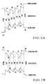
- Fig. 2A shows a state (non-bias state) wherein no forward bias voltage is applied
- Fig. 2B shows a state wherein forward bias voltage is applied.
- the p-type metal electrode 109 serves as an anode
- the n-type metal electrode 108 serves a cathode.
- An electron and hole constituting an exciton are respectively indicated by open and filled circles.
- the electron and hole constituting the exciton in the quantum-well layer 152 are spatially separated from each other.
- the distance between the electron and the hole changes as a forward bias voltage is applied.
- a forward bias voltage when a forward bias voltage is applied, the gradient of the band in the quantum-well layer 152 decreases, and the distance between the electron and the hole which constitute the exciton increases (the band-gap energy difference increases).
- the absorption edge wavelength of the exciton decreases as compared with a state wherein no voltage is applied.
- the wavelength of light incident on the light incident end of the semiconductor optical modulator is shorter than the absorption edge wavelength without any bias and longer than the absorption edge wavelength upon application of forward bias, the light is transmitted through the modulator and output only when forward bias is applied.
- the wavelength of light absorbed by the light absorption layer 105 changes upon application of a forward bias voltage.
- the semiconductor optical modulator according to this embodiment is a device that can be operated by applying a forward bias voltage, no crystal having high resistance to a reverse bias voltage is required unlike the conventional device. This makes it possible to simplify a crystal growth apparatus for manufacturing devices and simplify the crystal growth process as well. This can also improve the manufacturing yield of devices.
- TE polarized light is absorbed by both an exciton composed of a heavy hole and an electron and an exciton composed of a light hole and an electron
- TM polarized light is absorbed by only an exciton composed of a light hole and an electron.
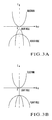
- Fig. 3A shows the band diagram of a wurtzite crystal which gives a tensile strain to a quantum-well layer having a quantum-well structure.
- the energy level of a light hole can be designed to be much lower than that of a heavy hole.
- the energy bands of the two holes can be made to coincide with each other.
- the degree of freedom in design of a band structure in the above wurtzite crystal is much higher than that in a zincblende crystal owing to the polarization effect within the crystal. It is therefore very easy to make the spectra generated by the two excitons coincide with each other in the absence of an electric field, as described above. This allows the optical modulator using the wurtzite crystal according to this embodiment to perform modulation without any light-polarization dependence.
- the direction of piezoelectric polarization produced by a tensile strain may coincide with or differ from the direction of spontaneous polarization of a wurtzite crystal. This is because the direction of spontaneous polarization depends on the polarity of a crystal. Depending on a combination of materials, therefore, the magnitude of spontaneous polarization may be equal to that of piezoelectric polarization, and hence the polarization effects may cancel each other. As a consequence, no electric field may be generated. In such a case, in order to obtain a polarization effect, materials must be combined such that the magnitude of piezoelectric polarization caused by a tensile strain differs from that of spontaneous polarization.
- Figs. 4A and 4B show the stacking orders of Ga and N atoms in a single crystal obtained by crystal growth of GaN along the c-axis.
- the stacking orders correspond to the polarities.
- a state wherein three N atoms combine with each other above a Ga atom when viewed from the surface of single-crystal GaN is called Ga polarity or +c polarity.
- a state wherein three Ga atoms combine with each other above an N atom when viewed from the surface of single-crystal GaN is called N polarity or -c polarity.
- This polarity is irrelevant to whether the surface of single-crystal GaN is composed of Ga or N atoms.
- adsorption atoms also exist in the surface of single-crystal GaN.
- N atoms may exist in the surface.
- the stacking order of atoms can be seen in consideration of the number of bonds between atoms. The internal structure remains unchanged regardless of phenomena on the surface and the kinds of atoms adsorbed on the surface, and hence the polarity of a crystal is uniquely determined.
- a polarization electric field is determined by the polarity.
- Polarization determined by the polarity is called spontaneous polarization.
- Figs. 4A and 4B show the relationship between the polarity and spontaneous polarization. If a grown crystal has the Ga polarity, an electric field generated by spontaneous polarization is directed from the inside of the crystal to its surface. If the grown crystal has the N polarity, the electric field generated by spontaneous polarization is directed from the surface of the crystal to its inside.
- the crystal lattice of GaN formed on the sapphire substrate contracts in a direction parallel to the interface and extends in a direction perpendicular to the interface, as shown in Fig. 4D.
- an electric field is generated by piezoelectric polarization in a direction perpendicular to the interface, i.e., a direction parallel to the c-axis.
- the direction of this piezoelectric polarization depends on the direction of a strain. In the case of compressive strain, the piezoelectric polarization is directed to the sapphire substrate (Fig. 4C). In the case of tensile strain, the piezoelectric polarization is opposite in direction to that in the case shown in Fig. 4C, i.e., directed from the sapphire substrate to the GaN layer.
- spontaneous polarization charges in AlN, GaN, and InN are 0.081, 0.029, and 0.032 C/m 2 . These values are much larger than the charge in a crystal having a perovskite structure which is a ferroelectric substance.
- e 33 and e 31 are piezoelectric coefficients, which have values shown in Table 1 given below. Piezoelectric Coefficients of Nitrides Semiconductors Material e 33 e 31 AlN 1.46 -0.60 GaN 0.73 -0.49 InN 0.92 -0.57
- the number of values shown in Table 1 is about 1/3 that of perovskite crystals.
- optical modulation can be done without applying a high reverse bias voltage.
- a state wherein polarization is produced in the absence of a bias can be obtained when, for example, spontaneous polarization is produced in the light absorption layer.
- a quantum-well layer is made of InGaN and a barrier layer is made of InGaAlN
- spontaneous polarization can be produced in the light absorption layer.
- InGaN and InGaAlN can have similar lattice constants unless the piezoelectric polarization is necessary.
- a state wherein polarization is produced in the absence of a bias can be obtained if spontaneous polarization and piezoelectric polarization are produced in the light absorption layer, and the sum of their magnitudes is not 0.
- a state wherein piezoelectric polarization is produced in addition to spontaneous polarization in the light absorption layer can be obtained if the lattice constant of the quantum-well layer differs from that of the barrier layer. If, however, spontaneous polarization and piezoelectric polarization are equal in magnitude and different in direction, since they cancel each other, a state wherein polarization is produced in the light absorption layer in the absence of a bias cannot be obtained.
- the equilibrium vapor pressure of nitrogen on the solid phase of InN is five orders of magnitude higher than those of the remaining compounds (see non-patent reference 5). It is almost impossible to form a high-quality crystal using InN having such characteristics by a method like reactive sputtering in which the pressure in a vessel (e.g., a vacuum chamber) used for the formation of a film cannot be increased.
- a vessel e.g., a vacuum chamber
- MOVPE metalorganic vapor phase epitaxy
- the first technical improvement to grow the above high-quality single-crystal InN was to form in advance GaN having an intermediate lattice constant between those of sapphire and InN on a sapphire substrate.
- a GaN layer is required to have high crystallinity.
- the growth conditions for GaN were optimized in the following points:
- the second technical improvement was to investigate the growth conditions for InN on GaN grown under the conditions optimized in the above manner.
- the items investigated were a growth temperature, a growth rate, the ratio of a Group V source to an In source, a gas flow rate in the reactor, and the like.
- the inventors made the first success in growing InN whose optical characteristics could be measured.
- an InN layer can be directly formed on a sapphire layer without forming any GaN template therebetween.
- Figs. 5 and 6 show the characteristics of a grown InN film.
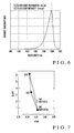
- Fig. 5 shows the relationship between absorbance squared and photon energy in the grown film, in which a clear absorption edge is detected from optical absorbance. Since this relationship is almost linear, InN can be regarded as a direct transition type, and the Eg can be estimated as about 0.8 eV.
- Fig. 6 shows the photoluminescence measured at room temperature from the InN film grown under the above conditions. It is obvious that light emission occurred near a wavelength of 1.59 ⁇ m (0.8 eV). Both the measurement results of absorbance and photoluminescence shown in Figs. 5 and 6 indicate that the Eg of the InN film grown under the above condition is 0.8 eV. From these results, it can be estimated that the Eg of InN is near 0.8 eV.
- Fig. 7 shows the relationship between the Eg of InGaAlN and a lattice constant a of the a-axis.
- compositions of the barrier layer 151 and quantum-well layer 152 constructing the light absorption layer 105 may therefore be properly selected such that the barrier layer 151 has a higher band-gap energy within the triangle defined by the three filled circles in Fig. 7.
- the quantum-well layer 152 may be made of undoped GaN and the barrier layer 151 may be made of undoped AlN.
- a combination of materials and a crystal growth process must be considered so as not to make the sum of the magnitudes of piezoelectric polarization and spontaneous polarization become 0.
- a metalorganic vapor phase epitaxy apparatus having a vertical-type reactor is used for crystal growth for the formation of each crystal layer.
- a nitrogen source ammonia is used.
- a carrier gas nitrogen gas is used for the growth of a quantum-well structure, and hydrogen gas is used for the growth of other crystal layers.
- the growth pressure is set to atmospheric pressure.
- the substrate temperature is set at 1,050°C, and the surface of the single-crystal substrate 101 made of sapphire is nitrided in an ammonia atmosphere to form a very thin nitride layer on the single-crystal substrate 101.
- the nitride layer is a very thin layer (not shown).
- the substrate temperature is set at 550°C, and the buffer layer 102 is formed by growing GaN.
- triethylgallium (TEG) is used as a gallium source, which has a relatively low gallium vapor pressure.
- the single-crystal substrate 101 is annealed at 1,050°C for 9 min to change the buffer layer 102 into a single crystal in the solid phase.
- the temperature of the single-crystal substrate is then set at 1,020°C, and Mg-doped p-type GaN and Mg-doped p-type Al 0.1 Ga 0.9 N are sequentially grown to form the electrode layer 103 and cladding layer 104, respectively.
- Mg-doped p-type GaN and Mg-doped p-type Al 0.1 Ga 0.9 N are sequentially grown to form the electrode layer 103 and cladding layer 104, respectively.
- TMA trimethylaluminum
- TMG trimethylgallium
- Mg doping methylcaptan biscyclopentadienylmagnesium (MeCP 2 Mg) is used. This source is a liquid, which is advantageous in reproducibility of the doping concentration of Mg over biscyclopentadienylmagnesium which is a generally used solid source.
- GaN and InN crystals are alternately grown on the cladding layer 104 to form a multilayer structure (MQW structure) constructed by the barrier layers 151 and quantum-well layers 152.
- MQW structure multilayer structure
- the growth temperature is set to, for example, 575°C.
- TMI trimethylindium
- the ratio of ammonia to TMI i.e., V/III
- Nitrogen is used both as a carrier gas and a bubbling gas. This is because the use of hydrogen as a carrier gas will suppress the decomposition of ammonia (see non-patent reference 5).
- Figs. 8A, 8B, and 8C show, as an example of the relationship between growth conditions for InN and crystallinity, the X-ray diffraction spectra of InN grown while a ratio V/III (ammonia/indium) of the amount of ammonia as a nitrogen source supplied to the reactor to the amount of trimethylindium (TMI) as an indium source supplied to the reactor is changed.
- Figs. 8A, 8B, and 8C show ⁇ -2 ⁇ scan spectra.
- V/III ammonia/indium
- TMI trimethylindium
- the barrier layer 151 When a GaN playing a role as the barrier layer 151 is to be grown on the high-quality InN crystal grown in the above manner, nitrogen is used as a carrier gas to prevent a deterioration in crystallinity upon etching InN, and the substrate temperature is set to 575°C, which is the same temperature as in the growth of InN.
- the substrate temperature is raised to 1,020°C to sequentially grow Si-doped n-type Al 01 Ga 0.9 N and Si-doped n-type GaN, thereby forming the cladding layer 106 and contact layer 107, respectively.
- Silane (SiH 4 ) gas which is diluted with hydrogen and has a concentration of 1 ppm is used to dope each layer with Si.
- the same source is used for Si doping in other processes.
- the resultant structure is annealed in a nitrogen atmosphere at 700°C for 30 min to activate Mg added to these layers.
- a 50-nm thick aluminum film and 20-nm thick gold film are sequentially deposited by using an electron beam deposition apparatus, thereby forming a metal layer serving as the n-type metal electrode 108.
- a novolac-based positive photoresist pattern is formed on the metal layer by the known photolithography technique.
- the lower layer is etched by using this pattern as a mask to form an exposed region on the electrode layer 103.
- the crystal layer may be etched by reactive ion etching using chlorine gas.
- a 50-nm thick nickel film and 200-nm thick gold film are sequentially deposited on the exposed region of the electrode layer 103, and the resultant structure is patterned to form the p-type metal electrode 109.
- the lower surface of the single-crystal substrate 101 is polished so as to thin the single-crystal substrate 101 to a thickness of 80 ⁇ m, and the lower surface is mirror-finished.
- the single-crystal substrate 101 is removed from the polishing base without mirror-finishing the lower surface, the single-crystal substrate 101 may warp or crack. For this reason, the lower surface is mirror-finished.
- the resultant structure is cleaned, and predetermined portions are cut by cleavage, thereby obtaining the semiconductor optical modulator with a device length of 1 mm shown Figs. 1A and 1B.
- GaN of the barrier layers 151 constructing the light absorption layer 105 is grown in the order of a nitrogen atom, gallium atom, nitrogen atom, and gallium atom in the direction from the lower surface of the single-crystal substrate 101 to the upper surface of it, i.e., in the order of a group V atom, group III atom, group V atom, and group III atom. This stacking order of atoms is generally called + (plus) polarity.
- the gradient of the band structure is in the reverse state to that in Fig. 2A.
- the gradient of each band structure has a gradient slanting to the right unlike the state shown in Fig. 2A.
- application of a reverse bias voltage will reduce the gradient of the band.
- each crystal layer can be formed with - polarity in the following manner even by using the same substrate as that used for the semiconductor optical modulator according to this embodiment.
- the surface of a c-plane sapphire substrate is nitrided in advance by exposing it to an ammonia atmosphere at a high temperature.
- a buffer layer made of GaN is grown on the sapphire substrate having undergone this nitridation process at a low temperature to a predetermined thickness.
- the growth process is then interrupted for a predetermined period of time. During this interruption of the grown process, the buffer layer which has already been formed is annealed at a high temperature of 1,000°C or higher.
- GaN is grown at a high temperature of 1,000°C or higher to form a single-crystal GaN layer with - polarity.
- This technique is known as a two-step growth method.
- the single-crystal GaN layer with - polarity formed in this manner has a rocking curve with of 40 sec or less, which is obtained by X-ray diffraction.
- Single-crystal GaN with + polarity has a rocking curve width of 100 sec or more. Obviously, therefore, as compared with this, the above single-crystal GaN layer with - polarity has good crystallinity.
- the modulator is operated with the n-type metal electrode 108 and p-type metal electrode 109 shown in Figs. 1A and 1B serving as a cathode and anode, respectively. That is, the modulator is operated while a voltage is applied to the diode in the forward direction. By applying a voltage in this manner, the gradient of the band of the quantum-well layer 152 made of InN shown in Fig. 2A can be reduced or leveled. Furthermore, the gradient can be reversed. In this embodiment, the modulator is operated without injecting any current.
- Fig. 9 shows the characteristics of this embodiment, i.e., the relationship between the applied modulation voltage and the transmitted light intensity.
- This semiconductor optical modulator is operated by a forward bias.
- the wavelength of light from a light source used to investigate the characteristics in Fig. 9 is 1.53 ⁇ m, and the intensity of light input into the device is 10 ⁇ W.
- the thickness of the quantum-well layer 152 and a combination of In 1-X-Y Ga X Al Y N (0 ⁇ X, Y ⁇ 1, 0 ⁇ X + Y ⁇ 1) compositions forming the quantum-well layers 152 and barrier layers 151 are properly designed in consideration of the polarization effect, thereby allowing the selection of a wavelength that can be modulated.
- a combination of In 1-X-Y Ga X Al Y N (0 ⁇ X, Y ⁇ 1, 0 ⁇ X + Y ⁇ 1) compositions to be used for a light absorption layer is determined in consideration of the phase separation.
- Fig. 10 shows the immiscible regions of InGaAlN obtained by experiment and calculation (see non-patent reference 6).
- the chain lines indicate the immiscible region of InGaAlN when it grows at 600°C; the solid lines, the immiscible region of InGaAlN when it grows at 800°C; and the dashed lines, the immiscible region of InGaAlN when it grows at 1,000°C.
- the regions inside the respective lines are the immiscible regions.
- compositions are determined in consideration of the condition of the miscible region shown in Fig. 10, an MQW structure using an InGaAlN-based material can be realized. Since InN and GaN that form the light absorption layer 105 in the embodiment shown in Figs. 1A and 1B are binary compounds, no phase separation like that described above occurs, providing conditions for easier manufacturing.
- the barrier layers 151 and quantum-well layers 152 are formed with their crystal lattice constants being mismatched.
- InGaAlN compositions may be determined in consideration of the characteristics of InGaAlN-based material shown in Fig. 7.
- a semiconductor laser diode with an optical modulator can be realized by monolithically integrating the semiconductor optical modulator of this embodiment shown in Figs. 1A and 1B with a semiconductor laser.
- an optical modulator of the external modulation scheme can be formed by forming an n-type GaN layer 1002 on an n-type semiconductor substrate 1001 and integrally forming, on the n-type GaN layer 1002, a waveguide-type semiconductor laser 1003 and a semiconductor optical modulator 1004 having the layer arrangement shown in Figs. 1A and 1B while the optical axes of the laser 1003 and the modulator 1004 are aligned with each other.
- the semiconductor laser 1003 is formed from general nitride semiconductor material.
- a common n-type electrode may be formed on the n-type GaN layer 1002, and p-type electrodes may be separately formed on the semiconductor laser 1003 and semiconductor optical modulator 1004.
- a common cathode can be formed to simplify the circuit arrangement. This allows optical modulation with higher frequencies.
- a space is ensured between the semiconductor laser 1003 and the semiconductor optical modulator 1004.
- the invention is not limited to this. These components may be arranged in tight contact with each other by using a known structure such as Butt-joint.
- the semiconductor laser 1003 may be optically coupled to the semiconductor optical modulator 1004 by another technique.
- the respective layers constituting the semiconductor laser 1003 are doped with various kinds of impurities. This, however, hardly affects semiconductor optical modulator 1004.
- the above structure may be operated as a reverse bias structure by applying a reverse bias.
- the electrode layer 103 shown in Figs. 1A and 1B is formed from n-type GaN.
- the cladding layer 104, cladding layer 106, and contact layer 107 are respectively formed from n-type Al 0.1 Ga 0.9 N, p-type Al 0.1 Ga 0.9 N, and p-type GaN.
- a p-type metal electrode is then formed on the contact layer 107, and an n-type metal electrode is formed on the electrode layer 103.
- the n-type metal electrode and p-type metal electrode can be operated as an anode and cathode, respectively.
- a metal electrode is directly formed on a semiconductor layer such as the contact layer 107.
- an insulating layer may be formed in place of the contact layer 107, and a metal electrode may be formed on the insulating layer. Forming this insulating film makes it possible to prevent injection of carriers into the light absorption layer 105 more reliably.
- a quantum-well layer of a light absorption layer may have a lattice constant smaller than that of a barrier layer, and the spontaneous polarization of the quantum-well layer may differ in magnitude from the piezoelectric polarization produced in the quantum-well layer.
- reverse bias can be applied most efficiently by making the directions of spontaneous polarization and piezoelectric polarization coincide with each other and also coincide with the direction of a reverse bias. If spontaneous polarization differs in direction from piezoelectric polarization, the sum of the two polarizations exists. It suffices if the direction of the sum coincides with the reverse bias direction.
- Fig. 12 schematically shows a semiconductor optical modulator in which a light absorption region in the form of a ridge is formed on the surface of a 300- ⁇ m thick substrate 1101 made of n-type GaN.
- the light absorption region is constructed by a lower cladding layer 1102 which is about 1.5 ⁇ m thick and made of Si-doped n-type Al 0.1 Ga 0.9 N, a 0.5- ⁇ m thick lower SCH (Separate Confinement Hetero) layer 1103 made of undoped InGaAlN, a light absorption layer 1104 having an MQW structure, a 5- ⁇ m thick upper SCH layer 1105 made of undoped InGaAlN, a 1.5- ⁇ m thick upper cladding layer 1106 made of Mg-doped p-type Al 0.1 Ga 0.9 N, and a 0.1- ⁇ m thick contact layer 1107 made of Mg-doped p-type GaN.
- a lower cladding layer 1102 which is about
- the light absorption layer 1104 is an MQW structure formed by alternately stacking well layers made of In 1-X-Y Ga X Al Y N (0 ⁇ X, Y ⁇ 1, 0 ⁇ X + Y ⁇ 1) and barrier layers made of In 1-X'-Y' Ga X' Al Y' N (0 ⁇ X', Y' ⁇ 1, 0 ⁇ X' + Y' ⁇ 1).
- polyimide layers 1110 are buried in two side portions of the light absorption region which is formed by stacking these layers so as to form a ridge structure.
- the upper surface of the contact layer 1107 is almost flush with the upper surface of the polyimide layer 1110.
- a p-type electrode 1108 having a multilayer structure constituted by a 50-nm thick nickel layer in direct contact with the contact layer 1107 and a 200-nm thick gold layer formed on the nickel layer is formed on the contact layer 1107.
- An n-type electrode 1109 having a multilayer structure constituted by a 50-nm thick aluminum layer in direct contact with the substrate 1101 and a 200-nm thick gold layer is formed on the lower surface of the substrate 1101.
- the semiconductor optical modulator has the SCH structure in which the cladding layers provided on the upper and lower surfaces of the light absorption layer 1104 are constituted by the lower cladding layer 1102, lower SCH layer 1103, upper SCH layer 1105, and upper cladding layer 1106.
- the incident light must be confined in the light absorption layer 1104. If the thickness of the light absorption region is about 1/10 or more the wavelength of light, light can be confined by using a double-heterostructure. In contrast to this, if the light absorption region has a thin quantum-well structure, light widely spreads in the cladding layer. As a consequence, the degree of confinement of light in the active layer decreases.
- a waveguide structure using the second cladding layer is the above SCH structure.
- the lower SCH layer 1103 and upper SCH layer 1105 correspond to the second cladding layer.
- the use of an SCH structure as in the semiconductor optical modulator in Fig. 12 enhances the effect of confining light in the light absorption layer, thereby improving the absorbance of the light absorption layer.
- the above cladding layer and second cladding layer used in the above SCH structure are configured to have larger band-gap energy than the active region (light absorption region).
- a reverse bias is applied
- the state shown in Fig. 2A is changed into the state shown in Fig. 13 wherein the gradient of the band increases, and the energy between an electron and a hole in a quantum-well layer 152 becomes lower than that in the absence of a bias.
- the absorption-edge wavelength increases. That is, if the wavelength of light incident on the light incident end of the semiconductor optical modulator in Figs. 1A and 1B is longer than the absorption edge wavelength in the absence of a bias and shorter than the absorption edge wavelength upon application of a revere bias, the light is transmitted through the modulator and output only when no bias is applied.
- the light absorption region is depleted by the built-in voltage generated upon formation of a polarization electric field and p-n junction. Therefore, optimal operation can be realized without externally applying a reverse bias DC voltage, and high-speed operation can be realized for modulation of high-intensity light without accumulating carriers.
- the upper and lower SCH layers and light absorption layer are depleted by a polarization electric field, the thickness of the upper and lower SCH layers can be reduced to the minimum necessary to confine light.
- Such reduction in thickness makes it possible to reduce the ineffective voltage components produced by the SCH layers, and allows an external modulation voltage to contribute to optical modulation very effectively. This can realize low-voltage driving.
- the number of MQW layers of a light absorption layer can be increased by the extent to which the upper and lower SCH layers are thinned. Therefore, the extinction characteristic can be changed more steeply with respect to voltage, thus realizing operation at lower voltages.
- a semiconductor optical device can be provided, which exhibits small nonlinearity with respect to driving voltage.
- each quantum-well layer is made of In 1-X-Y Ga X Al Y N (0 ⁇ X, Y ⁇ 1, 0 ⁇ X + Y ⁇ 1), and each barrier layer is made of In 1-X'-Y' Ga X' Al Y' N (0 ⁇ X', Y' ⁇ 1, 0 ⁇ X' + Y' ⁇ 1). Therefore, the light absorption layer is made of a material with a small Auger effect, and stands the influences of operating temperatures.
- Spontaneous polarization is always produced in a quantum-well layer serving as a light absorption layer.
- An electric field is generated in the light absorption layer even in the absence of a bias voltage so as to incline the gradient of the band of the quantum-well layer forming the light absorption layer.
- a bias voltage so as to incline the gradient of the band of the quantum-well layer forming the light absorption layer.
- the bonding energy of an exciton which is constituted with an electron and a hole can be increased, and the wavelength of absorbed light can be changed.
- modulation can be performed by operation using forward bias.
- the MQW layer is completely depleted by polarization electric field and the built-in voltage generated by the formation of a p-n junction, and optimal operation can be realized without externally applying a reverse bias voltage.
- low-modulation-voltage operation is realized, requirements for a driver for driving the modulator are reduced. This makes it possible to reduce the cost of the driver and power consumption. Therefore, great reductions in the size and cost of the transmission apparatus can be achieved.
- each barrier is set to be larger than that of each quantum-well layer to distort the quantum-well layer, thereby producing piezoelectric polarization in addition to the above spontaneous polarization.
- This makes it possible to generate an electric field in the light absorption layer even in the absence of a bias voltage and incline the gradient of the band of the quantum-well layer forming the light absorption layer.
- spontaneous polarization such as tensile strain differs in direction from piezoelectric polarization
- the compositions of each quantum-well layer and each barrier layer are combined to make the magnitude of the spontaneous polarization differ from that of the piezoelectric polarization.
Landscapes
- Physics & Mathematics (AREA)
- Nonlinear Science (AREA)
- Optics & Photonics (AREA)
- Chemical & Material Sciences (AREA)
- Engineering & Computer Science (AREA)
- Nanotechnology (AREA)
- General Physics & Mathematics (AREA)
- Life Sciences & Earth Sciences (AREA)
- Biophysics (AREA)
- Crystallography & Structural Chemistry (AREA)
- Optical Modulation, Optical Deflection, Nonlinear Optics, Optical Demodulation, Optical Logic Elements (AREA)
- Semiconductor Lasers (AREA)
Abstract
Description
Japanese Patent Laid-Open No. 8-86987
Fabio Bernardini, Vincenzo Fiorentini, and David Vanderbilt, "Spontaneous polarization and piezoelectric constants of III-V nitrides", Phys. Rev. B, 56 (1997) R10024
K. Osamura, K. Nakajima and Y. Murakami, "Fundamental absorption edge GaN, InN and their alloys", Solid State Comm., 11(1972)617
N. Puychevrier and M. Menoret, "Synthesis of III-V semiconductor nitrides by reactive cathodic sputtering", Thin Solid Films, 36(1976)141
T.L. Tansley and C.P. Foley, "Optical band gap of indium nitride", J. Appl. Phys., 59(1986)3241
T. Matsuoka, H. Tanaka, T. Sasaki and A. Katusi, "Wide-Gap Semiconductor (In, Ga) N", International Symposium on GaAs and Related Compounds, (Karuizawa, Japan, 1989); in Inst. Phys. Conf. Ser., 106. pp. 141 - 146
T. Matsuoka, "Phase Separation in Wurtzite In1-X-YGaXAlYN", MRS Internet J. Nitride Semicond. Res. 3,54(1998)
| Piezoelectric Coefficients of Nitrides Semiconductors | ||
| Material | e33 | e31 |
| AlN | 1.46 | -0.60 |
| GaN | 0.73 | -0.49 |
| InN | 0.92 | -0.57 |
Claims (19)
- A semiconductor optical modulator characterized by comprising at least:a lower cladding layer (104, 1102) of a first conductivity type;a light absorption layer (105, 1104) which is formed on said lower cladding layer and has a quantum-well structure constituted by a quantum-well layer (152) and a barrier layer (151); andan upper cladding layer (106, 1106) of a second conductivity type formed on said light absorption layer,wherein the quantum-well layer is made of In1-X-YGaXAlYN (0 ≦ X, Y ≦ 1, 0 ≦ X + Y ≦ 1),the barrier layers is made of In1-X'-Y'GaX'AlY'N (0 ≦ X', Y' ≦ 1, 0 ≦ X' + Y' ≦ 1), andan optical waveguide having a light incident end is constituted by said lower cladding layer, said light absorption layer, and said upper cladding layer.
- A modulator according to claim 1, wherein said light absorption layer includes a multiple-quantum-well structure.
- A modulator according to claim 1, wherein said lower cladding layer is formed on a predetermined substrate (101, 1101).
- A modulator according to claim 1, wherein polarization is produced in said light absorption layer in the absence of a bias.
- A modulator according to claim 4, wherein the polarization is spontaneous polarization produced in said light absorption layer.
- A modulator according to claim 4, wherein the polarization is the sum of spontaneous polarization and piezoelectric polarization produced in said light absorption layer.
- A modulator according to claim 4, wherein the quantum-well layer and the barrier layer have different lattice constants.
- A modulator according to claim 7, wherein the quantum-well layer has a larger lattice constant than the barrier layer.
- A modulator according to claim 7, wherein the quantum-well layer has a smaller lattice constant than the barrier layer.
- A modulator according to claim 4, wherein
the quantum-well layer comprises crystal InN, and
the barrier layer comprises crystal GaN. - A laser with an optical modulator, characterized by comprising a waveguide type semiconductor laser (1003) and a semiconductor optical modulator (1004) which are integrated on a single substrate (1001),
wherein said semiconductor optical modulator includes at least a lower cladding layer of a first conductivity type formed on a substrate, a light absorption layer which is formed on the lower cladding layer and has a quantum-well structure constituted by a quantum-well layer and a barrier layer, and an upper cladding layer of a second conductivity type formed on the light absorption layer, the quantum-well layer is made of In1-X-YGaXAlYN (0 ≦ X, Y ≦ 1, 0 ≦ X + Y ≦ 1), the barrier layers is made of In1-X'-Y'GaX'AlY'N (0 ≦ X', Y' ≦ 1, 0 ≦ X' + Y' ≦ 1), and an optical waveguide having a light incident end is constituted by the lower cladding layer, the light absorption layer, and the upper cladding layer. - A laser according to claim 11, wherein said optical modulator includes a multiple-quantum-well structure.
- A laser according to claim 11, wherein polarization is produced in the light absorption layer in the absence of a bias.
- A laser according to claim 13, wherein the polarization is spontaneous polarization produced in the light absorption layer.
- A laser according to claim 13, wherein the polarization is the sum of spontaneous polarization and piezoelectric polarization produced in the light absorption layer.
- A laser according to claim 13, wherein the quantum-well layer and the barrier layer have different lattice constants.
- A laser according to claim 16, wherein the quantum-well layer has a larger lattice constant than the barrier layer.
- A laser according to claim 16, wherein the quantum-well layer has a smaller lattice constant than the barrier layer.
- A laser according to claim 13, wherein
the quantum-well layer comprises crystal InN, and
the barrier layer comprises crystal GaN.
Applications Claiming Priority (2)
| Application Number | Priority Date | Filing Date | Title |
|---|---|---|---|
| JP2002269729 | 2002-09-17 | ||
| JP2002269729 | 2002-09-17 |
Publications (3)
| Publication Number | Publication Date |
|---|---|
| EP1400835A2 true EP1400835A2 (en) | 2004-03-24 |
| EP1400835A3 EP1400835A3 (en) | 2005-06-08 |
| EP1400835B1 EP1400835B1 (en) | 2011-11-16 |
Family
ID=31944515
Family Applications (1)
| Application Number | Title | Priority Date | Filing Date |
|---|---|---|---|
| EP03090300A Expired - Lifetime EP1400835B1 (en) | 2002-09-17 | 2003-09-16 | Semiconductor optical modulator and laser with such optical modulator |
Country Status (3)
| Country | Link |
|---|---|
| US (1) | US7039078B2 (en) |
| EP (1) | EP1400835B1 (en) |
| CN (1) | CN1288764C (en) |
Cited By (1)
| Publication number | Priority date | Publication date | Assignee | Title |
|---|---|---|---|---|
| FR2887373A1 (en) * | 2005-06-17 | 2006-12-22 | Thales Sa | OPTOELECTRONIC COMPONENT COMPRISING A SEMICONDUCTOR OPTICAL GUIDE WITH AN ENHANCED OPTICAL INDEX ACTIVE HEART |
Families Citing this family (19)
| Publication number | Priority date | Publication date | Assignee | Title |
|---|---|---|---|---|
| EP1885918B1 (en) * | 2005-05-11 | 2017-01-25 | North Carolina State University | Methods of preparing controlled polarity group iii-nitride films |
| JP2007019277A (en) * | 2005-07-07 | 2007-01-25 | Rohm Co Ltd | Semiconductor light emitting device |
| KR101041843B1 (en) * | 2005-07-30 | 2011-06-17 | 삼성엘이디 주식회사 | Nitride compound semiconductor light emitting device and manufacturing method thereof |
| CN100474642C (en) * | 2005-10-27 | 2009-04-01 | 晶能光电(江西)有限公司 | Indium gallium aluminium nitrogen semi-conductor luminous element containing metallic chromium substrate and manufacturing method thereof |
| KR100818487B1 (en) * | 2006-01-19 | 2008-04-02 | 삼성전기주식회사 | Projection system using semiconductor diode |
| US7508858B2 (en) * | 2007-04-30 | 2009-03-24 | The Research Foundation Of State University Of New York | Detuned duo-cavity laser-modulator device and method with detuning selected to minimize change in reflectivity |
| TWI341600B (en) * | 2007-08-31 | 2011-05-01 | Huga Optotech Inc | Light optoelectronic device and forming method thereof |
| EP2464760A4 (en) | 2009-08-12 | 2013-08-28 | Univ Georgia State Res Found | APPARATUS AND METHODS FOR HIGH PRESSURE CHEMICAL METHOD VAPOR DEPOSITION, AND COMPOSITIONS PRODUCED THEREFROM |
| CN101788726B (en) * | 2010-03-30 | 2012-12-05 | 华中科技大学 | Semiconductor full gloss polarization switch |
| WO2013150748A1 (en) * | 2012-04-05 | 2013-10-10 | パナソニック株式会社 | Optical modulator, optical pickup, and optical modulation module |
| CN103151435B (en) * | 2013-01-30 | 2015-05-06 | 东南大学 | Gallium nitride base light-emitting diode with composite potential barrier |
| US9224599B2 (en) | 2013-12-31 | 2015-12-29 | Industrial Technology Research Institute | P-type metal oxide semiconductor material and method for fabricating the same |
| KR101848804B1 (en) * | 2015-07-10 | 2018-04-16 | 한양대학교 에리카산학협력단 | Optical module, optical transceiver and communication system including the same |
| US20170047708A1 (en) * | 2015-08-12 | 2017-02-16 | Finisar Corporation | Wavefunction deconfinement electro-absorption modulator |
| US10454239B2 (en) * | 2015-08-28 | 2019-10-22 | International Business Machines Corporation | Wafer scale monolithic integration of lasers, modulators, and other optical components using ALD optical coatings |
| CN108063365B (en) * | 2017-12-12 | 2020-11-13 | 中国科学院半导体研究所 | Preparation method of electrically pumped perovskite quantum dot laser |
| US11329450B2 (en) * | 2019-08-19 | 2022-05-10 | Lumentum Japan, Inc. | Electro-absorption optical modulator and manufacturing method thereof |
| US11909172B2 (en) * | 2020-01-08 | 2024-02-20 | Asahi Kasei Kabushiki Kaisha | Method for manufacturing optical device and optical device |
| CN119297740B (en) * | 2024-10-10 | 2026-03-06 | 安徽格恩半导体有限公司 | GaN-based compound semiconductor laser element |
Family Cites Families (19)
| Publication number | Priority date | Publication date | Assignee | Title |
|---|---|---|---|---|
| GB1579818A (en) * | 1977-06-07 | 1980-11-26 | Yamanouchi Pharma Co Ltd | Nifedipine-containing solid preparation composition |
| FR2602423B1 (en) * | 1986-08-08 | 1989-05-05 | Ethypharm Sa | PROCESS FOR THE PREPARATION OF A FENOFIBRATE-BASED MEDICINAL PRODUCT, OBTAINED BY THIS PROCESS |
| FR2627696B1 (en) * | 1988-02-26 | 1991-09-13 | Fournier Innovation Synergie | NEW GALENIC FORM OF FENOFIBRATE |
| US4992277A (en) * | 1989-08-25 | 1991-02-12 | Schering Corporation | Immediate release diltiazem formulation |
| FR2722984B1 (en) * | 1994-07-26 | 1996-10-18 | Effik Lab | PROCESS FOR THE PREPARATION OF DRY PHARMACEUTICAL FORMS AND THE PHARMACEUTICAL COMPOSITIONS THUS PRODUCED |
| JPH0878786A (en) * | 1994-09-02 | 1996-03-22 | Mitsubishi Electric Corp | Strained quantum well structure |
| JPH0886978A (en) | 1994-09-16 | 1996-04-02 | Sumitomo Electric Ind Ltd | Optical circulator and light control method |
| US5545628A (en) * | 1995-01-10 | 1996-08-13 | Galephar P.R. Inc. | Pharmaceutical composition containing fenofibrate |
| US5963358A (en) | 1995-04-26 | 1999-10-05 | Kabushiki Kaisha Toshiba | Semiconductor device and method for its operation |
| SI9500173B (en) * | 1995-05-19 | 2002-02-28 | Lek, | Three-phase pharmaceutical form with constant and controlled release of amorphous active ingredient for single daily application |
| JP3080889B2 (en) | 1996-09-02 | 2000-08-28 | 日本電気株式会社 | Semiconductor laser |
| SE507376C2 (en) | 1996-09-04 | 1998-05-18 | Ericsson Telefon Ab L M | Wavelength tunable laser device |
| JP3904709B2 (en) | 1997-02-21 | 2007-04-11 | 株式会社東芝 | Nitride-based semiconductor light-emitting device and method for manufacturing the same |
| US6180138B1 (en) * | 1999-01-29 | 2001-01-30 | Abbott Laboratories | Process for preparing solid formulations of lipid-regulating agents with enhanced dissolution and absorption |
| GB9912583D0 (en) | 1999-05-28 | 1999-07-28 | Arima Optoelectronics Corp | A light emitting diode having a two well system with asymmetric tunneling |
| JP3719047B2 (en) | 1999-06-07 | 2005-11-24 | 日亜化学工業株式会社 | Nitride semiconductor device |
| GB2352085A (en) | 1999-07-15 | 2001-01-17 | Univ Bristol | Integrated semiconductor optical devices |
| JP3626423B2 (en) | 2000-05-22 | 2005-03-09 | 日本碍子株式会社 | Photonic device manufacturing method |
| US6526083B1 (en) * | 2001-10-09 | 2003-02-25 | Xerox Corporation | Two section blue laser diode with reduced output power droop |
-
2003
- 2003-09-16 CN CNB031588794A patent/CN1288764C/en not_active Expired - Lifetime
- 2003-09-16 EP EP03090300A patent/EP1400835B1/en not_active Expired - Lifetime
- 2003-09-16 US US10/665,515 patent/US7039078B2/en not_active Expired - Lifetime
Cited By (2)
| Publication number | Priority date | Publication date | Assignee | Title |
|---|---|---|---|---|
| FR2887373A1 (en) * | 2005-06-17 | 2006-12-22 | Thales Sa | OPTOELECTRONIC COMPONENT COMPRISING A SEMICONDUCTOR OPTICAL GUIDE WITH AN ENHANCED OPTICAL INDEX ACTIVE HEART |
| WO2006134053A3 (en) * | 2005-06-17 | 2007-08-09 | Thales Sa | Optoelectronic component comprising a semiconductor optical guide with an active core with enhanced optical index |
Also Published As
| Publication number | Publication date |
|---|---|
| EP1400835B1 (en) | 2011-11-16 |
| US20040062282A1 (en) | 2004-04-01 |
| US7039078B2 (en) | 2006-05-02 |
| CN1490644A (en) | 2004-04-21 |
| EP1400835A3 (en) | 2005-06-08 |
| CN1288764C (en) | 2006-12-06 |
Similar Documents
| Publication | Publication Date | Title |
|---|---|---|
| US7039078B2 (en) | Semiconductor optical modulator and laser with optical modulator | |
| US6072197A (en) | Semiconductor light emitting device with an active layer made of semiconductor having uniaxial anisotropy | |
| US6924512B2 (en) | Nitride semiconductor light-emitting device and optical apparatus including the same | |
| Chang et al. | InGaN-GaN multiquantum-well blue and green light-emitting diodes | |
| EP1014455B1 (en) | Nitride semiconductor device | |
| US6377597B1 (en) | Gallium nitride semiconductor light emitting element with active layer having multiplex quantum well structure and semiconductor laser light source device | |
| US6677619B1 (en) | Nitride semiconductor device | |
| EP1389814B1 (en) | Semiconductor light-emitting device | |
| JP4166885B2 (en) | Optical semiconductor device and manufacturing method thereof | |
| US5548128A (en) | Direct-gap germanium-tin multiple-quantum-well electro-optical devices on silicon or germanium substrates | |
| EP1178543A1 (en) | Semiconductor light emitting device | |
| EP0896406A2 (en) | Semiconductor laser device, optical communication system using the same, and method for producing compound semiconductor | |
| JP2002335052A (en) | Nitride semiconductor device | |
| KR20060114683A (en) | Baan-based III-VIII compound semiconductor light emitting device and method of manufacturing the same | |
| KR20070107609A (en) | Semiconductor lasers, methods for manufacturing semiconductor devices, optical pickups, and optical disk devices | |
| JP4072107B2 (en) | Semiconductor optical modulator and laser with optical modulator | |
| KR100277310B1 (en) | Nitride compound semiconductor laser device and laser device using same | |
| US5519721A (en) | Multi-quantum well (MQW) structure laser diode/modulator integrated light source | |
| WO2015103266A1 (en) | Monolithic integration of optically pumped iii-nitride devices | |
| JP3716395B2 (en) | Semiconductor light emitting device | |
| Nakamura | Materials issues for InGaN-based lasers | |
| AU765732B2 (en) | Nitride semiconductor device | |
| Khoo et al. | Piezoelectric InGaAs/AlGaAs laser with intracavity absorber | |
| Klude et al. | New laser sources for plastic optical fibers: ZnSe-based quantum well and quantum dot laser diodes with 560-nm emission | |
| JP2001028473A (en) | Method for growing n-type nitride semiconductor |
Legal Events
| Date | Code | Title | Description |
|---|---|---|---|
| PUAI | Public reference made under article 153(3) epc to a published international application that has entered the european phase |
Free format text: ORIGINAL CODE: 0009012 |
|
| AK | Designated contracting states |
Kind code of ref document: A2 Designated state(s): AT BE BG CH CY CZ DE DK EE ES FI FR GB GR HU IE IT LI LU MC NL PT RO SE SI SK TR |
|
| AX | Request for extension of the european patent |
Extension state: AL LT LV MK |
|
| PUAL | Search report despatched |
Free format text: ORIGINAL CODE: 0009013 |
|
| AK | Designated contracting states |
Kind code of ref document: A3 Designated state(s): AT BE BG CH CY CZ DE DK EE ES FI FR GB GR HU IE IT LI LU MC NL PT RO SE SI SK TR |
|
| AX | Request for extension of the european patent |
Extension state: AL LT LV MK |
|
| 17P | Request for examination filed |
Effective date: 20050601 |
|
| AKX | Designation fees paid |
Designated state(s): DE FR GB |
|
| 17Q | First examination report despatched |
Effective date: 20060803 |
|
| GRAP | Despatch of communication of intention to grant a patent |
Free format text: ORIGINAL CODE: EPIDOSNIGR1 |
|
| GRAS | Grant fee paid |
Free format text: ORIGINAL CODE: EPIDOSNIGR3 |
|
| RIN1 | Information on inventor provided before grant (corrected) |
Inventor name: FUKANO,HIDEKINTT INTELLECTUAL PROPERTY CENTER Inventor name: MATSUOKA,TAKASHINTT INTELLECTUAL PROPERTY CENTER |
|
| GRAA | (expected) grant |
Free format text: ORIGINAL CODE: 0009210 |
|
| AK | Designated contracting states |
Kind code of ref document: B1 Designated state(s): DE FR GB |
|
| REG | Reference to a national code |
Ref country code: GB Ref legal event code: FG4D |
|
| REG | Reference to a national code |
Ref country code: DE Ref legal event code: R096 Ref document number: 60339118 Country of ref document: DE Effective date: 20120209 |
|
| PLBE | No opposition filed within time limit |
Free format text: ORIGINAL CODE: 0009261 |
|
| STAA | Information on the status of an ep patent application or granted ep patent |
Free format text: STATUS: NO OPPOSITION FILED WITHIN TIME LIMIT |
|
| 26N | No opposition filed |
Effective date: 20120817 |
|
| REG | Reference to a national code |
Ref country code: DE Ref legal event code: R097 Ref document number: 60339118 Country of ref document: DE Effective date: 20120817 |
|
| REG | Reference to a national code |
Ref country code: FR Ref legal event code: PLFP Year of fee payment: 14 |
|
| REG | Reference to a national code |
Ref country code: FR Ref legal event code: PLFP Year of fee payment: 15 |
|
| REG | Reference to a national code |
Ref country code: FR Ref legal event code: PLFP Year of fee payment: 16 |
|
| PGFP | Annual fee paid to national office [announced via postgrant information from national office to epo] |
Ref country code: GB Payment date: 20220920 Year of fee payment: 20 Ref country code: DE Payment date: 20220920 Year of fee payment: 20 |
|
| PGFP | Annual fee paid to national office [announced via postgrant information from national office to epo] |
Ref country code: FR Payment date: 20220922 Year of fee payment: 20 |
|
| REG | Reference to a national code |
Ref country code: DE Ref legal event code: R071 Ref document number: 60339118 Country of ref document: DE |
|
| REG | Reference to a national code |
Ref country code: GB Ref legal event code: PE20 Expiry date: 20230915 |
|
| PG25 | Lapsed in a contracting state [announced via postgrant information from national office to epo] |
Ref country code: GB Free format text: LAPSE BECAUSE OF EXPIRATION OF PROTECTION Effective date: 20230915 |