EP1400360A1 - Exposure head and image forming apparatus using the same - Google Patents
Exposure head and image forming apparatus using the same Download PDFInfo
- Publication number
- EP1400360A1 EP1400360A1 EP03025773A EP03025773A EP1400360A1 EP 1400360 A1 EP1400360 A1 EP 1400360A1 EP 03025773 A EP03025773 A EP 03025773A EP 03025773 A EP03025773 A EP 03025773A EP 1400360 A1 EP1400360 A1 EP 1400360A1
- Authority
- EP
- European Patent Office
- Prior art keywords
- light
- exposure head
- organic
- substrate
- array
- Prior art date
- Legal status (The legal status is an assumption and is not a legal conclusion. Google has not performed a legal analysis and makes no representation as to the accuracy of the status listed.)
- Withdrawn
Links
- 239000000758 substrate Substances 0.000 claims abstract description 32
- 238000007641 inkjet printing Methods 0.000 claims abstract description 24
- 238000005192 partition Methods 0.000 claims description 28
- 230000015572 biosynthetic process Effects 0.000 claims description 9
- 239000010409 thin film Substances 0.000 claims description 7
- 238000004519 manufacturing process Methods 0.000 abstract description 8
- 239000010410 layer Substances 0.000 description 41
- 229910052799 carbon Inorganic materials 0.000 description 26
- 239000000203 mixture Substances 0.000 description 18
- 239000000463 material Substances 0.000 description 14
- 238000000034 method Methods 0.000 description 14
- 238000002347 injection Methods 0.000 description 11
- 239000007924 injection Substances 0.000 description 11
- 238000000576 coating method Methods 0.000 description 9
- 239000010408 film Substances 0.000 description 8
- XLYOFNOQVPJJNP-UHFFFAOYSA-N water Substances O XLYOFNOQVPJJNP-UHFFFAOYSA-N 0.000 description 8
- 239000011248 coating agent Substances 0.000 description 6
- 230000001276 controlling effect Effects 0.000 description 6
- 230000003287 optical effect Effects 0.000 description 6
- 238000004140 cleaning Methods 0.000 description 4
- 238000001704 evaporation Methods 0.000 description 4
- 239000011521 glass Substances 0.000 description 4
- 239000011368 organic material Substances 0.000 description 4
- 230000008020 evaporation Effects 0.000 description 3
- 239000007789 gas Substances 0.000 description 3
- 238000003384 imaging method Methods 0.000 description 3
- 239000012212 insulator Substances 0.000 description 3
- 230000002093 peripheral effect Effects 0.000 description 3
- 230000002940 repellent Effects 0.000 description 3
- 239000005871 repellent Substances 0.000 description 3
- 239000002904 solvent Substances 0.000 description 3
- 239000004925 Acrylic resin Substances 0.000 description 2
- 229920000178 Acrylic resin Polymers 0.000 description 2
- IJGRMHOSHXDMSA-UHFFFAOYSA-N Atomic nitrogen Chemical compound N#N IJGRMHOSHXDMSA-UHFFFAOYSA-N 0.000 description 2
- 239000004642 Polyimide Substances 0.000 description 2
- XLOMVQKBTHCTTD-UHFFFAOYSA-N Zinc monoxide Chemical compound [Zn]=O XLOMVQKBTHCTTD-UHFFFAOYSA-N 0.000 description 2
- 229910021417 amorphous silicon Inorganic materials 0.000 description 2
- 238000003491 array Methods 0.000 description 2
- 238000010276 construction Methods 0.000 description 2
- 239000006059 cover glass Substances 0.000 description 2
- 238000000151 deposition Methods 0.000 description 2
- 230000008021 deposition Effects 0.000 description 2
- 238000010586 diagram Methods 0.000 description 2
- 239000003822 epoxy resin Substances 0.000 description 2
- NBVXSUQYWXRMNV-UHFFFAOYSA-N fluoromethane Chemical compound FC NBVXSUQYWXRMNV-UHFFFAOYSA-N 0.000 description 2
- 238000010438 heat treatment Methods 0.000 description 2
- 229910010272 inorganic material Inorganic materials 0.000 description 2
- 239000011147 inorganic material Substances 0.000 description 2
- 239000011229 interlayer Substances 0.000 description 2
- 238000005468 ion implantation Methods 0.000 description 2
- 238000000206 photolithography Methods 0.000 description 2
- 238000009832 plasma treatment Methods 0.000 description 2
- 229910021420 polycrystalline silicon Inorganic materials 0.000 description 2
- 229920000647 polyepoxide Polymers 0.000 description 2
- 229920001721 polyimide Polymers 0.000 description 2
- 229920005591 polysilicon Polymers 0.000 description 2
- 235000019353 potassium silicate Nutrition 0.000 description 2
- 238000007639 printing Methods 0.000 description 2
- 239000011241 protective layer Substances 0.000 description 2
- 230000001105 regulatory effect Effects 0.000 description 2
- 238000004528 spin coating Methods 0.000 description 2
- 238000005507 spraying Methods 0.000 description 2
- 238000007738 vacuum evaporation Methods 0.000 description 2
- ZOXJGFHDIHLPTG-UHFFFAOYSA-N Boron Chemical compound [B] ZOXJGFHDIHLPTG-UHFFFAOYSA-N 0.000 description 1
- MYMOFIZGZYHOMD-UHFFFAOYSA-N Dioxygen Chemical compound O=O MYMOFIZGZYHOMD-UHFFFAOYSA-N 0.000 description 1
- VYPSYNLAJGMNEJ-UHFFFAOYSA-N Silicium dioxide Chemical compound O=[Si]=O VYPSYNLAJGMNEJ-UHFFFAOYSA-N 0.000 description 1
- 239000004809 Teflon Substances 0.000 description 1
- 229920006362 Teflon® Polymers 0.000 description 1
- 239000012298 atmosphere Substances 0.000 description 1
- 229910052796 boron Inorganic materials 0.000 description 1
- 239000006229 carbon black Substances 0.000 description 1
- 239000003086 colorant Substances 0.000 description 1
- 239000002131 composite material Substances 0.000 description 1
- 239000000470 constituent Substances 0.000 description 1
- 238000007796 conventional method Methods 0.000 description 1
- 238000002425 crystallisation Methods 0.000 description 1
- 230000008025 crystallization Effects 0.000 description 1
- 239000002274 desiccant Substances 0.000 description 1
- 238000007607 die coating method Methods 0.000 description 1
- 229910001882 dioxygen Inorganic materials 0.000 description 1
- 238000003618 dip coating Methods 0.000 description 1
- 238000007598 dipping method Methods 0.000 description 1
- 238000005516 engineering process Methods 0.000 description 1
- BHEPBYXIRTUNPN-UHFFFAOYSA-N hydridophosphorus(.) (triplet) Chemical compound [PH] BHEPBYXIRTUNPN-UHFFFAOYSA-N 0.000 description 1
- 239000012535 impurity Substances 0.000 description 1
- 229910003437 indium oxide Inorganic materials 0.000 description 1
- PJXISJQVUVHSOJ-UHFFFAOYSA-N indium(iii) oxide Chemical compound [O-2].[O-2].[O-2].[In+3].[In+3] PJXISJQVUVHSOJ-UHFFFAOYSA-N 0.000 description 1
- 238000005342 ion exchange Methods 0.000 description 1
- 238000001459 lithography Methods 0.000 description 1
- 239000011159 matrix material Substances 0.000 description 1
- 238000002156 mixing Methods 0.000 description 1
- 229910052757 nitrogen Inorganic materials 0.000 description 1
- 238000000059 patterning Methods 0.000 description 1
- 229920002120 photoresistant polymer Polymers 0.000 description 1
- 229920000642 polymer Polymers 0.000 description 1
- 230000035945 sensitivity Effects 0.000 description 1
- 229910052814 silicon oxide Inorganic materials 0.000 description 1
- 229910052709 silver Inorganic materials 0.000 description 1
- 238000004544 sputter deposition Methods 0.000 description 1
- 229910001220 stainless steel Inorganic materials 0.000 description 1
- 239000010935 stainless steel Substances 0.000 description 1
- MZLGASXMSKOWSE-UHFFFAOYSA-N tantalum nitride Chemical compound [Ta]#N MZLGASXMSKOWSE-UHFFFAOYSA-N 0.000 description 1
- XOLBLPGZBRYERU-UHFFFAOYSA-N tin dioxide Chemical compound O=[Sn]=O XOLBLPGZBRYERU-UHFFFAOYSA-N 0.000 description 1
- 229910001887 tin oxide Inorganic materials 0.000 description 1
- 239000011787 zinc oxide Substances 0.000 description 1
Images



Classifications
-
- B—PERFORMING OPERATIONS; TRANSPORTING
- B41—PRINTING; LINING MACHINES; TYPEWRITERS; STAMPS
- B41J—TYPEWRITERS; SELECTIVE PRINTING MECHANISMS, i.e. MECHANISMS PRINTING OTHERWISE THAN FROM A FORME; CORRECTION OF TYPOGRAPHICAL ERRORS
- B41J2/00—Typewriters or selective printing mechanisms characterised by the printing or marking process for which they are designed
- B41J2/435—Typewriters or selective printing mechanisms characterised by the printing or marking process for which they are designed characterised by selective application of radiation to a printing material or impression-transfer material
- B41J2/447—Typewriters or selective printing mechanisms characterised by the printing or marking process for which they are designed characterised by selective application of radiation to a printing material or impression-transfer material using arrays of radiation sources
- B41J2/45—Typewriters or selective printing mechanisms characterised by the printing or marking process for which they are designed characterised by selective application of radiation to a printing material or impression-transfer material using arrays of radiation sources using light-emitting diode [LED] or laser arrays
- B41J2/451—Special optical means therefor, e.g. lenses, mirrors, focusing means
-
- B—PERFORMING OPERATIONS; TRANSPORTING
- B41—PRINTING; LINING MACHINES; TYPEWRITERS; STAMPS
- B41J—TYPEWRITERS; SELECTIVE PRINTING MECHANISMS, i.e. MECHANISMS PRINTING OTHERWISE THAN FROM A FORME; CORRECTION OF TYPOGRAPHICAL ERRORS
- B41J2/00—Typewriters or selective printing mechanisms characterised by the printing or marking process for which they are designed
- B41J2/005—Typewriters or selective printing mechanisms characterised by the printing or marking process for which they are designed characterised by bringing liquid or particles selectively into contact with a printing material
- B41J2/01—Ink jet
-
- B—PERFORMING OPERATIONS; TRANSPORTING
- B41—PRINTING; LINING MACHINES; TYPEWRITERS; STAMPS
- B41J—TYPEWRITERS; SELECTIVE PRINTING MECHANISMS, i.e. MECHANISMS PRINTING OTHERWISE THAN FROM A FORME; CORRECTION OF TYPOGRAPHICAL ERRORS
- B41J2/00—Typewriters or selective printing mechanisms characterised by the printing or marking process for which they are designed
- B41J2/435—Typewriters or selective printing mechanisms characterised by the printing or marking process for which they are designed characterised by selective application of radiation to a printing material or impression-transfer material
- B41J2/447—Typewriters or selective printing mechanisms characterised by the printing or marking process for which they are designed characterised by selective application of radiation to a printing material or impression-transfer material using arrays of radiation sources
- B41J2/45—Typewriters or selective printing mechanisms characterised by the printing or marking process for which they are designed characterised by selective application of radiation to a printing material or impression-transfer material using arrays of radiation sources using light-emitting diode [LED] or laser arrays
-
- H—ELECTRICITY
- H10—SEMICONDUCTOR DEVICES; ELECTRIC SOLID-STATE DEVICES NOT OTHERWISE PROVIDED FOR
- H10K—ORGANIC ELECTRIC SOLID-STATE DEVICES
- H10K59/00—Integrated devices, or assemblies of multiple devices, comprising at least one organic light-emitting element covered by group H10K50/00
- H10K59/80—Constructional details
- H10K59/875—Arrangements for extracting light from the devices
-
- B—PERFORMING OPERATIONS; TRANSPORTING
- B41—PRINTING; LINING MACHINES; TYPEWRITERS; STAMPS
- B41J—TYPEWRITERS; SELECTIVE PRINTING MECHANISMS, i.e. MECHANISMS PRINTING OTHERWISE THAN FROM A FORME; CORRECTION OF TYPOGRAPHICAL ERRORS
- B41J2202/00—Embodiments of or processes related to ink-jet or thermal heads
- B41J2202/01—Embodiments of or processes related to ink-jet heads
- B41J2202/09—Ink jet technology used for manufacturing optical filters
-
- H—ELECTRICITY
- H10—SEMICONDUCTOR DEVICES; ELECTRIC SOLID-STATE DEVICES NOT OTHERWISE PROVIDED FOR
- H10K—ORGANIC ELECTRIC SOLID-STATE DEVICES
- H10K50/00—Organic light-emitting devices
- H10K50/80—Constructional details
- H10K50/85—Arrangements for extracting light from the devices
-
- H—ELECTRICITY
- H10—SEMICONDUCTOR DEVICES; ELECTRIC SOLID-STATE DEVICES NOT OTHERWISE PROVIDED FOR
- H10K—ORGANIC ELECTRIC SOLID-STATE DEVICES
- H10K59/00—Integrated devices, or assemblies of multiple devices, comprising at least one organic light-emitting element covered by group H10K50/00
Definitions
- the present invention relates to an exposure head and to an image forming apparatus using the same.
- the exposure head may comprise an organic electroluminescent (hereinafter abbreviated as "EL") array. More particularly, the present invention relates to an exposure head integrated with image-forming lenses and also pertains to an image forming apparatus using the same.
- EL organic electroluminescent
- JP (A) Hei 10-55890
- the whole organic EL array is fabricated on an insulating substrate, e.g. glass, and a separate driver IC is combined with the organic EL array.
- a converging rod lens array is used to image the light-emitting parts of the organic EL array onto a photosensitive drum.
- JP (A) Hei 11-198433 uses a one-chip organic EL array having a plurality of rows of light-emitting parts.
- an EL layer of the organic EL array is deposited by evaporation.
- microlenses are formed on the top surface of a substrate by an ion exchange method.
- microlenses are formed on the bottom surface of a substrate by a method using a photoresist or by a replica method.
- An organic EL array having a resonator structure is deposited in alignment with the microlenses by evaporation.
- JP (A) Hei 10-12377 relates to a method of producing an active matrix organic EL display.
- An organic light-emitting layer is formed by ink-jet printing over a glass substrate having thin-film transistors.
- JP (A) 2000-323276 a hole injection layer and an organic light-emitting layer of an organic EL element are formed by coating using ink-jet printing with a partition wall provided therearound.
- JP (A) 2001-18441 a light-emitting layer and a TFT layer for controlling light emission therefrom are formed in a photosensitive drum to construct a printer.
- JP(A) Hei 10-55890 and Hei 11-198433 need to use a separate optical system. This causes the apparatus to increase in size and cost unavoidably.
- the present invention was made in view of the above-described problems with the prior art.
- An object of the present invention is to provide an exposure head integrated with microlenses for converging or diverging light from light-emitting parts, together with a method of fabricating the exposure head and an image forming apparatus using the same.
- the present invention provides an exposure head including an array of light-emitting parts arranged in the form of at least one row of pixels on a substrate of continuous length.
- the exposure head further includes a microlens formed by inkjet printing over a surface of each light-emitting part at a side thereof remote from the substrate.
- the organic EL light-emitting parts should be formed in respective discrete holes divided from each other by a partition wall provided on the substrate, and the microlens should be formed over each of the light-emitting parts in the holes.
- a thin-film electronic circuit for controlling light emission from the light-emitting parts should be formed on the substrate, and the light-emitting parts should be provided over the thin-film electronic circuit.
- An (organic) light-emitting layer and a hole injection layer constituting the light-emitting parts may also be formed by ink-jet printing.
- microlens should be a convex lens.
- the present invention provides a method of fabricating an exposure head.
- reflector electrodes are formed in the form of at least one row of pixels on a substrate of continuous length.
- Each reflector electrode constitutes one electrode of each light-emitting part.
- a partition wall of a predetermined height is formed over the reflector electrodes.
- the partition wall has discrete holes corresponding to the reflector electrodes.
- an (organic) light-emitting layer or a hole injection layer constituting each light-emitting part is formed in each hole in the partition wall by ink-jet printing.
- a hole injection layer or an (organic) light-emitting layer constituting each light-emitting part is formed in each hole in the partition wall by ink-jet printing.
- a transparent electrode is formed uniformly over a surface of the substrate as the other electrode of each light-emitting part.
- microlens is formed over the transparent electrode in each hole in the partition wall by ink-jet printing.
- a surface thereof may be treated to be water repellent so that a convex lens is formed thereon as a microlens.
- the surface of the transparent electrode may be treated to be hydrophilic so that a concave lens is formed thereon as a microlens.
- a thin-film electronic circuit for controlling light emission from the light-emitting parts should be formed on the substrate.
- the present invention includes image forming apparatus having the above-described exposure head as an exposure head for writing an image on an image carrier.
- image forming apparatus having the above-described exposure head as an exposure head for writing an image on an image carrier.
- One example is a tandem color image forming apparatus including at least two image forming stations each having an electric charging device, an exposure head, a developing device, and a transfer device around an image carrier, wherein a transfer medium passes through the stations to perform color image formation.
- the exposure head according to the present invention has an array of light- emitting parts arranged in the form of at least one row of pixels on a substrate of continuous length.
- the exposure head further has a microlens formed by inkjet printing over a surface of each light-emitting part at a side thereof remote from the substrate. Accordingly, it is possible to readily provide a low-cost exposure head for use in electrophotographic printers, etc. that suffers minimal unevenness of exposure and has a simplified arrangement requiring no separate optical system.
- An embodiment of an exposure head having an organic EL array according to the present invention will be described below on the basis of a method of fabricating the same.
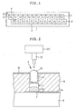
- Fig. 1 is a schematic plan view of an embodiment of an organic EL array exposure head according to the present invention.
- Fig. 2 is a sectional view of one pixel in an array taken along the straight line A-A' in Fig. 1.
- the organic EL array exposure head 1 in this embodiment has two parallel arrays 2 and 2' of staggered pixels 3.
- the arrays 2 and 2' each comprises a large number of pixels 3 arranged in a straight-line form.
- Each pixel 3 has the same structure formed from an organic EL light-emitting part 4 and a TFT 5 for controlling light emission from the organic EL light-emitting part 4.
- Fig. 2 is a sectional view showing one pixel 3, including an organic EL light-emitting part 4 and a TFT 5.
- the organic EL array exposure head 1 will be described below in the order of the fabrication sequence.
- TFT's 5 are fabricated on a glass substrate 6.
- Various methods of making TFT's 5 are known. For example, a silicon oxide film is deposited on the glass substrate 6 first. Then, an amorphous silicon film is deposited thereon. Next, the amorphous silicon film is irradiated with an excimer laser beam for crystallization to form a polysilicon film serving as a channel. After the polysilicon film has been patterned, a gate insulator is deposited thereover.
- a gate electrode made of tantalum nitride is formed.
- source and drain regions of n-channel TFT's are formed by ion implantation of phosphorous
- source and drain regions of p-channel TFT's are formed by ion implantation of boron.
- the following fabrication steps are carried out successively: deposition of a first interlayer insulator; opening of first contact holes; formation of source wires; deposition of a second interlayer insulator; opening of second contact holes; and formation of metallic pixel electrodes.
- each metallic pixel electrode serves as a cathode 7 of each organic EL light-emitting part 4, and also serves as a reflector layer of the organic EL light-emitting part 4.
- the pixel electrodes are formed from metallic thin-film electrodes of Mg, Ag, Al, Li, etc.
- a partition wall (bank) 9 of a predetermined height is formed.
- the partition wall 9 has a hole 8 corresponding to each organic EL light-emitting part 4.
- the partition wall 9 can be made by a desired method, e.g. photolithography, or printing, as disclosed in JP(A) 2000-353594.
- a lithography process for example, an organic material is applied to the substrate surface to the height of the bank to be made by a predetermined method, e.g. spin coating, spray coating, roll coating, die coating, or dip coating, and a resist layer is applied to the surface of the applied organic material.
- the resist is exposed through a mask having a pattern corresponding to the configuration of the partition wall 9 to be made, and then developed, thereby allowing the resist to remain in a pattern corresponding to the configuration of the partition wall 9. Finally, the partition material is etched to remove the material from the area except the masked regions. It is also possible to form a bank (projection) comprising two or more layers, of which a lower layer is made of an inorganic material, and an upper layer is an organic material layer. JP(A) 2000-323276 discloses that the constituent material of the partition wall 9 is preferably an organic material, e.g.
- an acrylic resin, an epoxy resin, or a photosensitive polyimide because these materials can be formed into Teflon by fluorocarbon gas plasma treatment, although there is no particular restriction on the material of the partition wall 9, provided that the material used has durability with respect to a solvent used in the EL material. It is also possible to use a stacked partition structure having a lower layer made of an inorganic material, e.g. liquid glass. It is desirable that the partition wall 9 should be made black or opaque by mixing the above-described material with carbon black or the like. It becomes possible by making the partition wall 9 opaque to prevent crosstalk in which undesired light enters a neighboring pixel position.
- the substrate 6 provided with the partition wall 9 is subjected to continuous plasma treatment with oxygen gas and fluorocarbon gas plasma.
- the surface of the polyimide constituting the partition wall 9 is made water repellent, for example, whereas the surface of the cathode 7 is made hydrophilic.
- a plasma-generating apparatus it is possible to use either an apparatus that generates a plasma in a vacuum or an apparatus generating a plasma in the atmosphere.
- an ink composition for forming a light-emitting layer is jetted from a head 21 of an ink-jet printing apparatus 20 into each hole 8 in the partition wall 9 to apply a patterned coating to the surface of the cathode 7 of each pixel.
- the solvent is removed, and heat treatment is performed to form a light-emitting layer 10.
- ink-jet printing means to include the following printing processes: piezo ink-jet printing in which an ink composition is jetted out by using the mechanical energy of a piezoelectric element or the like; and thermal ink-jet printing in which an air bubble is generated by using the heat energy of a heater, and an ink composition is jetted out on the basis of the generation of the air bubble
- piezo ink-jet printing in which an ink composition is jetted out by using the mechanical energy of a piezoelectric element or the like
- thermal ink-jet printing in which an air bubble is generated by using the heat energy of a heater, and an ink composition is jetted out on the basis of the generation of the air bubble
- An ink-jet head 21 has a nozzle plate 22 and a diaphragm 23, which are made of stainless steel, for example.
- the nozzle plate 22 and the diaphragm 23 are joined together through partition members (reservoir plates) 24. Between the nozzle plate 22 and the diaphragm 23, a plurality of ink chambers 25 and reservoirs (not shown) are formed by the partition members 24.
- the interiors of the ink chambers 25 and the reservoirs are filled with an ink composition.
- the ink chambers 25 and the reservoirs communicate with each other through respective supply ports.
- the nozzle plate 22 is provided with nozzle openings 26 for spraying the ink composition from the ink chambers 25 in the form of jets.
- the ink-jet head 21 is formed with an ink inlet for supplying the ink composition to each reservoir.
- Piezoelectric elements 28 are joined to a surface of the diaphragm 23 opposite to a surface thereof facing the ink chambers 25 at respective positions corresponding to the ink chambers 25.
- Each piezoelectric element 28 is positioned between a pair of electrodes 29.
- the piezoelectric element 28 When energized, the piezoelectric element 28 is distorted so as to project outwardly. This causes the ink chamber 25 to increase in volume. Consequently, an amount of ink composition corresponding to the increase in volume of the ink chamber 25 flows thereinto from the reservoir through the supply port.
- the piezoelectric element 28 returns to its previous shape, together with the diaphragm 23. Consequently, the ink chamber 25 also returns to its previous volume. Therefore, the pressure of the ink composition in the ink chamber 25 increases, causing the ink composition to jet out from the nozzle opening 26 toward the substrate 6 provided with the partition wall
- an ink composition for forming a hole injection layer is jetted from the head 21 of the ink-jet printing apparatus 20 onto the light-emitting layer 10 in each hole 8 to apply a patterned coating to the surface of the light-emitting layer 10 of each pixel.
- the solvent is removed, and heat treatment is performed to form a hole injection layer 11.
- the order in which the light-emitting layer 10 and the hole injection layer 11 are stacked may be reverse to the above. It is desirable that a layer more resistant to water should be disposed closer to the surface side (i.e. more away from the substrate 6).
- the light-emitting layer 10 and the hole injection layer 11 can also be formed by a publicly known spin coating, dipping or evaporation method instead of applying the ink compositions by ink-jet printing as stated above.
- a transparent electrode 12 is deposited over the whole surface of the substrate 6 by vacuum evaporation to form an anode of the organic EL array.
- materials usable as the transparent electrode 12 include a tin oxide film, an ITO film, and a composite oxide film of indium oxide and zinc oxide. It is possible to use photolithography, sputtering or pyrosol process, for example, in addition to vacuum evaporation. With such a process, the transparent electrode 12 is formed over the top surface of the partition wall 9 and the inner surface of each hole 8.
- the surface of the transparent electrode 12 is treated to be water repellent.
- a transparent ink composition for forming a microlens is jetted from the head 21 of the ink-jet printing apparatus 20 into each hole 8 of the partition wall 9 to apply a patterned coating.
- the applied ink composition is cured to form a convex microlens 13 over the organic EL light-emitting part 4 of each pixel.
- the focal length is determined by the amount of ink composition jetted from the printer head 21, the diameter of the hole 8, the surface tension of the microlens-forming transparent ink composition, the degree of water repellency imparted to the transparent electrode 12, the rate of shrinkage of the ink composition when cured, etc.
- a concave microlens 14 can be formed over the organic EL light-emitting part 4 of each pixel, as shown in Fig. 4, by applying a patterned coating of a transparent ink composition in the same way as the above after the surface of the transparent electrode 12 has been treated to be hydrophilic.
- the organic EL light-emitting part 4 comprising the cathode 7, the light-emitting layer 10, the hole injection layer 11 and the transparent electrode (anode) 12 is easily deteriorated by water. Therefore, it is desirable that, as shown in Fig. 5(a), a transparent protective layer 15 should be applied to the whole surface of the substrate after the formation of the microlenses 13 or 14 to prevent the entry of water.
- a transparent protective layer 15 examples include an epoxy resin, an acrylic resin, and liquid glass.
- the arrangement may be such that the substrate surface is hermetically covered with a cover glass 16 after the formation of the microlenses 13 or 14, and a gas 17, e.g. nitrogen, is sealed in the space defined inside the cover glass 16, and a drying agent 18 is put in the space.
- a gas 17, e.g. nitrogen is sealed in the space defined inside the cover glass 16, and a drying agent 18 is put in the space.
- the organic EL array exposure head 1 has an array of organic EL light-emitting parts 4 provided on the substrate 6, together with an array of TFT's 5 for controlling light emission from the organic EL light-emitting parts 4.
- a convex microlens 13 with a predetermined focal length is formed over each organic EL light-emitting part 4 by ink-jet printing.
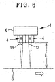
- the organic EL array exposure head 1 collects light beams emitted from the organic EL light-emitting parts 4 on a surface S a predetermined distance L away from the exposure head 1 in the same array pattern as that of the pixels 3 of the exposure head 1.
- a predetermined pattern can be recorded on the surface S by moving the surface S relative to the organic EL array exposure head 1 in a direction perpendicular to the longitudinal direction of the exposure head 1 and, at the same time, controlling the light emission from the organic EL light-emitting parts 4 of the exposure head 1 through the TFT's 5.
- the organic EL array exposure head 1 of the present invention is used as an exposure head of an electrophotographic color image forming apparatus, by way of example.
- Fig. 7 is a front view schematically showing the general arrangement of an example of a tandem color image forming apparatus in which four similar organic EL array exposure heads 1K, 1C, 1M and 1Y according to the present invention are disposed at the respective exposure positions of four similar photosensitive drums 41K, 41C, 41M and 41Y corresponding thereto. As shown in Fig.
- the image forming apparatus has an intermediate transfer belt 50 stretched between a driving roller 51 and a driven roller 52 with tension applied thereto by a tension roller 53 and driven to circulate in the direction of the arrows shown in the figure (counterclockwise direction) by the driving roller 51.
- Four photosensitive members 41K, 41C, 41M and 41Y are disposed at predetermined spacings with respect to the intermediate transfer belt 50.
- Each photosensitive member has a photosensitive layer on the outer peripheral surface thereof to serve as an image carrier.
- Suffixes "K”, “C”, “M”, and “Y” added to reference numeral 41 indicate black, cyan, magenta, and yellow, respectively. That is, the reference symbols denote photosensitive members for black, cyan, magenta, and yellow, respectively.
- the photosensitive members 41K, 41C, 41M and 41Y are driven to rotate in the direction of the arrows shown in the figure (clockwise direction) synchronously with the driving of the intermediate transfer belt 50.
- a charging device (corona charger) 42 K, C, M, and Y) for uniformly electrically charging the outer peripheral surface of the photosensitive member 41 (K, C, M, and Y
- an organic EL array exposure head 1 K, C, M, and Y
- a developing device 44 K, C, M, and Y
- Each organic EL array exposure head 1 (K, C, M, and Y), as shown in Fig. 6, has a convex microlens 13 with a predetermined focal length formed over each organic EL light-emitting part 4 by ink-jet printing, and is installed a predetermined distance L away from the surface of the associated photosensitive member 41 (K, C, M, and Y) in such a manner that the array direction of the organic EL array exposure head 1 (K, C, M, and Y) is parallel to the generator of the photosensitive member 41 (K, C, M, and Y).
- the emission energy peak wavelength of each organic EL array exposure head 1 and the sensitivity peak wavelength of the photosensitive member 41 (K, C, M, and Y) are set so as to be approximately coincident with each other.
- the developing device 44 uses a non-magnetic one-component toner as a developer, for example.
- the one-component developer is conveyed to a developing roller through a supply roller, for example, and the thickness of the developer layer adhering to the developing roller surface is regulated with a regulating blade.
- the developing roller is brought into contact with or pressed against the photosensitive member 41 (K, C, M, and Y) to allow the developer to adhere to the surface of the photosensitive member 41 (K, C, M, and Y) according to the electric potential level thereof, thereby developing the electrostatic latent image into a toner image.
- Toner images of black, cyan, magenta and yellow formed by single-color toner image forming stations for the four colors are sequentially primarily transferred onto the intermediate transfer belt 50 by a primary transfer bias applied to each primary transfer roller 45 (K, C, M, and Y), and sequentially superimposed on one another on the intermediate transfer belt 50 to form a full-color toner image, which is then secondarily transferred onto a recording medium P, e.g. a sheet of paper, at a secondary transfer roller 66.
- the transferred full-color toner image is fixed on the recording medium P by passing between a pair of fixing rollers 61 constituting a fixing part. Then, the recording medium P is discharged through a pair of sheet delivery rollers 62 onto a sheet delivery tray 68 formed on the top of the apparatus body.
- reference numeral 63 in Fig. 7 denotes a sheet cassette in which a stack of large number of recording media P is held.
- a pickup roller 64 feeds the recording media P from the sheet cassette 63 one by one.
- a pair of gate rollers 65 regulates the timing at which each recording medium P is supplied to the secondary transfer part formed between the secondary transfer roller (secondary transfer means) 66 and the intermediate transfer belt 50.
- a cleaning blade 67 serves as cleaning means for removing the toner remaining on the surface of the intermediate transfer belt 50 after the secondary transfer.
- the organic EL array exposure head 1 (K, C, M, and Y) used in the apparatus shown in Fig. 7 has a convex microlens 13 with a predetermined focal length formed over each organic EL light-emitting part 4 by ink-jet printing, as shown in Fig. 2.
- the image forming apparatus may use organic EL array exposure heads having a concave microlens 14 formed over each organic EL light-emitting part 4, as shown in Fig. 4.
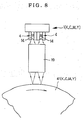
- an image-forming optical system 19 comprising a converging rod lens array, for example, should be disposed between the organic EL array exposure head 1 (K, C, M, and Y) and the photosensitive member 41 (K, C, M, and Y).
- the organic EL array exposure head has an array of organic EL light-emitting parts arranged in the form of at least one row of pixels on a substrate of continuous length.
- the organic EL array exposure head further has a microlens formed by ink-jet printing over a surface of each organic EL light-emitting part at a side thereof remote from the substrate. Accordingly, it is possible to readily provide a low-cost exposure head for use in electrophotographic printers, etc. that suffers minimal unevenness of exposure and has a simplified arrangement requiring no separate optical system.
Landscapes
- Physics & Mathematics (AREA)
- Optics & Photonics (AREA)
- Health & Medical Sciences (AREA)
- General Health & Medical Sciences (AREA)
- Toxicology (AREA)
- Printers Or Recording Devices Using Electromagnetic And Radiation Means (AREA)
- Electroluminescent Light Sources (AREA)
- Facsimile Heads (AREA)
Abstract
Description
- The present invention relates to an exposure head and to an image forming apparatus using the same. As exaplained below, the exposure head may comprise an organic electroluminescent (hereinafter abbreviated as "EL") array. More particularly, the present invention relates to an exposure head integrated with image-forming lenses and also pertains to an image forming apparatus using the same.
- Various techniques of using an organic EL array as an exposure head for image forming apparatus have heretofore been proposed. Those concerned therewith are as follows.
- In Japanese Patent Application Unexamined Publication Number [hereinafter referred to as "JP (A)"] Hei 10-55890, the whole organic EL array is fabricated on an insulating substrate, e.g. glass, and a separate driver IC is combined with the organic EL array. A converging rod lens array is used to image the light-emitting parts of the organic EL array onto a photosensitive drum.
- JP (A) Hei 11-198433 uses a one-chip organic EL array having a plurality of rows of light-emitting parts.
- However, the optical system for imaging the light-emitting parts onto a photosensitive drum is not clear. It should be noted that an EL layer of the organic EL array is deposited by evaporation.
- In JP (A) 2000-77188, microlenses are formed on the top surface of a substrate by an ion exchange method. Alternatively, microlenses are formed on the bottom surface of a substrate by a method using a photoresist or by a replica method. An organic EL array having a resonator structure is deposited in alignment with the microlenses by evaporation.
- JP (A) Hei 10-12377 relates to a method of producing an active matrix organic EL display. An organic light-emitting layer is formed by ink-jet printing over a glass substrate having thin-film transistors.
- In JP (A) 2000-323276, a hole injection layer and an organic light-emitting layer of an organic EL element are formed by coating using ink-jet printing with a partition wall provided therearound.
- In JP (A) 2001-18441, a light-emitting layer and a TFT layer for controlling light emission therefrom are formed in a photosensitive drum to construct a printer.
- When an organic EL array is used as an exposure head of a printer, e.g. an electrophotographic printer, in the above-described prior art, JP(A) Hei 10-55890 and Hei 11-198433 need to use a separate optical system. This causes the apparatus to increase in size and cost unavoidably. JP(A) 2000-77188, in which the organic EL array is integrated with microlenses, suffers problems such as a restriction in usable microlens materials. Further, these conventional techniques involve problems such as a narrow selectivity of materials for the EL layer because it is formed by evaporation.
- The present invention was made in view of the above-described problems with the prior art.
- An object of the present invention is to provide an exposure head integrated with microlenses for converging or diverging light from light-emitting parts, together with a method of fabricating the exposure head and an image forming apparatus using the same.
- To attain the above-described object, the present invention provides an exposure head including an array of light-emitting parts arranged in the form of at least one row of pixels on a substrate of continuous length. The exposure head further includes a microlens formed by inkjet printing over a surface of each light-emitting part at a side thereof remote from the substrate.
- In this case, it is desirable that the organic EL light-emitting parts should be formed in respective discrete holes divided from each other by a partition wall provided on the substrate, and the microlens should be formed over each of the light-emitting parts in the holes.
- It is also desirable that a thin-film electronic circuit for controlling light emission from the light-emitting parts should be formed on the substrate, and the light-emitting parts should be provided over the thin-film electronic circuit.
- An (organic) light-emitting layer and a hole injection layer constituting the light-emitting parts may also be formed by ink-jet printing.
- It is desirable that the microlens should be a convex lens.
- In addition, the present invention provides a method of fabricating an exposure head. According to the fabrication method, reflector electrodes are formed in the form of at least one row of pixels on a substrate of continuous length. Each reflector electrode constitutes one electrode of each light-emitting part.
- Then, a partition wall of a predetermined height is formed over the reflector electrodes. The partition wall has discrete holes corresponding to the reflector electrodes. Then, an (organic) light-emitting layer or a hole injection layer constituting each light-emitting part is formed in each hole in the partition wall by ink-jet printing.
- Then, a hole injection layer or an (organic) light-emitting layer constituting each light-emitting part is formed in each hole in the partition wall by ink-jet printing.
- Then, a transparent electrode is formed uniformly over a surface of the substrate as the other electrode of each light-emitting part.
- Thereafter, a microlens is formed over the transparent electrode in each hole in the partition wall by ink-jet printing.
- In this case, after the formation of the transparent electrode, a surface thereof may be treated to be water repellent so that a convex lens is formed thereon as a microlens. Alternatively, the surface of the transparent electrode may be treated to be hydrophilic so that a concave lens is formed thereon as a microlens.
- It is desirable that prior to the formation of the reflector electrodes, a thin-film electronic circuit for controlling light emission from the light-emitting parts should be formed on the substrate.
- The present invention includes image forming apparatus having the above-described exposure head as an exposure head for writing an image on an image carrier. One example is a tandem color image forming apparatus including at least two image forming stations each having an electric charging device, an exposure head, a developing device, and a transfer device around an image carrier, wherein a transfer medium passes through the stations to perform color image formation.
- Thus, the exposure head according to the present invention has an array of light-
emitting parts arranged in the form of at least one row of pixels on a substrate of continuous length. The exposure head further has a microlens formed by inkjet printing over a surface of each light-emitting part at a side thereof remote from the substrate. Accordingly, it is possible to readily provide a low-cost exposure head for use in electrophotographic printers, etc. that suffers minimal unevenness of exposure and has a simplified arrangement requiring no separate optical system. - Still other objects and advantages of the invention will in part be obvious and will in part be apparent from the specification.
- The invention accordingly comprises the features of construction, combinations of elements, and arrangement of parts which will be exemplified in the construction hereinafter set forth, and the scope of the invention will be indicated in the claims.
-
- Fig. 1 is a schematic plan view of an embodiment of an organic EL array exposure head according to the present invention.
- Fig. 2 is a sectional view of one pixel in an array shown in Fig. 1.
- Fig. 3 is a diagram showing a structural example of a piezo ink-jet printing head among ink-jet printing heads.
- Fig. 4 is a sectional view of one pixel in an array in which a concave microlens is formed over an organic EL light-emitting part of each pixel.
- Figs. 5(a) and 5(b) are sectional views of examples of a structure for preventing the entry of water.
- Fig. 6 is a sectional view showing the way in which light is collected by the organic EL array exposure head according to the present invention.
- Fig. 7 is a front view schematically showing the general arrangement of an example of a tandem color image forming apparatus equipped with organic EL array exposure heads according to the present invention.
- Fig. 8 is a diagram showing an example in which an image-forming optical system comprising a converging rod lens array is disposed between an organic EL array exposure head and a photosensitive drum.
-
- An embodiment of an exposure head having an organic EL array according to the present invention will be described below on the basis of a method of fabricating the same.
- Fig. 1 is a schematic plan view of an embodiment of an organic EL array exposure head according to the present invention. Fig. 2 is a sectional view of one pixel in an array taken along the straight line A-A' in Fig. 1.
- The organic EL
array exposure head 1 in this embodiment has twoparallel arrays 2 and 2' of staggeredpixels 3. Thearrays 2 and 2' each comprises a large number ofpixels 3 arranged in a straight-line form. Eachpixel 3 has the same structure formed from an organic EL light-emittingpart 4 and aTFT 5 for controlling light emission from the organic EL light-emittingpart 4. - Fig. 2 is a sectional view showing one
pixel 3, including an organic EL light-emittingpart 4 and aTFT 5. The organic ELarray exposure head 1 will be described below in the order of the fabrication sequence. First, TFT's 5 are fabricated on aglass substrate 6. Various methods of making TFT's 5 are known. For example, a silicon oxide film is deposited on theglass substrate 6 first. Then, an amorphous silicon film is deposited thereon. Next, the amorphous silicon film is irradiated with an excimer laser beam for crystallization to form a polysilicon film serving as a channel. After the polysilicon film has been patterned, a gate insulator is deposited thereover. Then, a gate electrode made of tantalum nitride is formed. Subsequently, source and drain regions of n-channel TFT's are formed by ion implantation of phosphorous, and source and drain regions of p-channel TFT's are formed by ion implantation of boron. After the ion-implanted impurities have been activated, the following fabrication steps are carried out successively: deposition of a first interlayer insulator; opening of first contact holes; formation of source wires; deposition of a second interlayer insulator; opening of second contact holes; and formation of metallic pixel electrodes. In this way, an array of TFT's 5 is completed [see, for example, "Polymer EL Display", The 8th Electronic Display Forum (April 18, 2001)]. It should be noted that each metallic pixel electrode serves as acathode 7 of each organic EL light-emittingpart 4, and also serves as a reflector layer of the organic EL light-emittingpart 4. The pixel electrodes are formed from metallic thin-film electrodes of Mg, Ag, Al, Li, etc. - Next, a partition wall (bank) 9 of a predetermined height is formed. The
partition wall 9 has ahole 8 corresponding to each organic EL light-emittingpart 4. Thepartition wall 9 can be made by a desired method, e.g. photolithography, or printing, as disclosed in JP(A) 2000-353594. When a lithography process is used, for example, an organic material is applied to the substrate surface to the height of the bank to be made by a predetermined method, e.g. spin coating, spray coating, roll coating, die coating, or dip coating, and a resist layer is applied to the surface of the applied organic material. The resist is exposed through a mask having a pattern corresponding to the configuration of thepartition wall 9 to be made, and then developed, thereby allowing the resist to remain in a pattern corresponding to the configuration of thepartition wall 9. Finally, the partition material is etched to remove the material from the area except the masked regions. It is also possible to form a bank (projection) comprising two or more layers, of which a lower layer is made of an inorganic material, and an upper layer is an organic material layer. JP(A) 2000-323276 discloses that the constituent material of thepartition wall 9 is preferably an organic material, e.g. an acrylic resin, an epoxy resin, or a photosensitive polyimide, because these materials can be formed into Teflon by fluorocarbon gas plasma treatment, although there is no particular restriction on the material of thepartition wall 9, provided that the material used has durability with respect to a solvent used in the EL material. It is also possible to use a stacked partition structure having a lower layer made of an inorganic material, e.g. liquid glass. It is desirable that thepartition wall 9 should be made black or opaque by mixing the above-described material with carbon black or the like. It becomes possible by making thepartition wall 9 opaque to prevent crosstalk in which undesired light enters a neighboring pixel position. - Immediately before the application of an ink composition for forming an organic EL light-emitting layer, the
substrate 6 provided with thepartition wall 9 is subjected to continuous plasma treatment with oxygen gas and fluorocarbon gas plasma. By doing so, the surface of the polyimide constituting thepartition wall 9 is made water repellent, for example, whereas the surface of thecathode 7 is made hydrophilic. Thus, it is possible to control the wettability of the substrate side for finely patterning ink-jet drops. As a plasma-generating apparatus, it is possible to use either an apparatus that generates a plasma in a vacuum or an apparatus generating a plasma in the atmosphere. - Next, an ink composition for forming a light-emitting layer is jetted from a
head 21 of an ink-jet printing apparatus 20 into eachhole 8 in thepartition wall 9 to apply a patterned coating to the surface of thecathode 7 of each pixel. After the coating process, the solvent is removed, and heat treatment is performed to form a light-emittinglayer 10. - The term "ink-jet printing" as used in the present invention means to include the following printing processes: piezo ink-jet printing in which an ink composition is jetted out by using the mechanical energy of a piezoelectric element or the like; and thermal ink-jet printing in which an air bubble is generated by using the heat energy of a heater, and an ink composition is jetted out on the basis of the generation of the air bubble ("Fine Imaging and Hardcopy", page 43, edited by Joint Publishing Committee between The Society of Photographic Science and Technology of Japan and The Imaging Society of Japan, published on January 7, 1999 by Corona Publishing Co., Ltd.). A structural example of a head used in piezo ink-jet printing is shown in Fig. 3. An ink-
jet head 21 has anozzle plate 22 and adiaphragm 23, which are made of stainless steel, for example. Thenozzle plate 22 and thediaphragm 23 are joined together through partition members (reservoir plates) 24. Between thenozzle plate 22 and thediaphragm 23, a plurality ofink chambers 25 and reservoirs (not shown) are formed by thepartition members 24. The interiors of theink chambers 25 and the reservoirs are filled with an ink composition. Theink chambers 25 and the reservoirs communicate with each other through respective supply ports. Further, thenozzle plate 22 is provided withnozzle openings 26 for spraying the ink composition from theink chambers 25 in the form of jets. The ink-jet head 21 is formed with an ink inlet for supplying the ink composition to each reservoir.Piezoelectric elements 28 are joined to a surface of thediaphragm 23 opposite to a surface thereof facing theink chambers 25 at respective positions corresponding to theink chambers 25. Eachpiezoelectric element 28 is positioned between a pair ofelectrodes 29. When energized, thepiezoelectric element 28 is distorted so as to project outwardly. This causes theink chamber 25 to increase in volume. Consequently, an amount of ink composition corresponding to the increase in volume of theink chamber 25 flows thereinto from the reservoir through the supply port. When deenergized, thepiezoelectric element 28 returns to its previous shape, together with thediaphragm 23. Consequently, theink chamber 25 also returns to its previous volume. Therefore, the pressure of the ink composition in theink chamber 25 increases, causing the ink composition to jet out from thenozzle opening 26 toward thesubstrate 6 provided with thepartition wall 9. - After the formation of the light-emitting
layer 10 in thehole 8, an ink composition for forming a hole injection layer is jetted from thehead 21 of the ink-jet printing apparatus 20 onto the light-emittinglayer 10 in eachhole 8 to apply a patterned coating to the surface of the light-emittinglayer 10 of each pixel. After the coating process, the solvent is removed, and heat treatment is performed to form ahole injection layer 11. - It should be noted that the order in which the light-emitting
layer 10 and thehole injection layer 11 are stacked may be reverse to the above. It is desirable that a layer more resistant to water should be disposed closer to the surface side (i.e. more away from the substrate 6). - The light-emitting
layer 10 and thehole injection layer 11 can also be formed by a publicly known spin coating, dipping or evaporation method instead of applying the ink compositions by ink-jet printing as stated above. - Regarding materials used to form the light-emitting
layer 10 and thehole injection layer 11, it is possible to use various publicly known materials, for example, those disclosed in JP(A) Hei-10-12377 and 2000-323276. A detailed description thereof is omitted herein. - After the light-emitting
layer 10 and thehole injection layer 11 have been successively formed in eachhole 8 of thepartition wall 9, atransparent electrode 12 is deposited over the whole surface of thesubstrate 6 by vacuum evaporation to form an anode of the organic EL array. Examples of materials usable as thetransparent electrode 12 include a tin oxide film, an ITO film, and a composite oxide film of indium oxide and zinc oxide. It is possible to use photolithography, sputtering or pyrosol process, for example, in addition to vacuum evaporation. With such a process, thetransparent electrode 12 is formed over the top surface of thepartition wall 9 and the inner surface of eachhole 8. - Next, the surface of the
transparent electrode 12 is treated to be water repellent. Then, a transparent ink composition for forming a microlens is jetted from thehead 21 of the ink-jet printing apparatus 20 into eachhole 8 of thepartition wall 9 to apply a patterned coating. After the coating process, the applied ink composition is cured to form aconvex microlens 13 over the organic EL light-emittingpart 4 of each pixel. The curvature radius of the surface of theconvex microlens 13, i.e. the focal length, is determined by the amount of ink composition jetted from theprinter head 21, the diameter of thehole 8, the surface tension of the microlens-forming transparent ink composition, the degree of water repellency imparted to thetransparent electrode 12, the rate of shrinkage of the ink composition when cured, etc. - It should be noted that a
concave microlens 14 can be formed over the organic EL light-emittingpart 4 of each pixel, as shown in Fig. 4, by applying a patterned coating of a transparent ink composition in the same way as the above after the surface of thetransparent electrode 12 has been treated to be hydrophilic. - Incidentally, the organic EL light-emitting
part 4 comprising thecathode 7, the light-emittinglayer 10, thehole injection layer 11 and the transparent electrode (anode) 12 is easily deteriorated by water. Therefore, it is desirable that, as shown in Fig. 5(a), a transparentprotective layer 15 should be applied to the whole surface of the substrate after the formation of themicrolenses protective layer 15 include an epoxy resin, an acrylic resin, and liquid glass. - As shown in Fig. 5(b), the arrangement may be such that the substrate surface is hermetically covered with a
cover glass 16 after the formation of themicrolenses gas 17, e.g. nitrogen, is sealed in the space defined inside thecover glass 16, and adrying agent 18 is put in the space. - Thus, the organic EL
array exposure head 1 according to the present invention has an array of organic EL light-emittingparts 4 provided on thesubstrate 6, together with an array of TFT's 5 for controlling light emission from the organic EL light-emittingparts 4. In addition, aconvex microlens 13 with a predetermined focal length is formed over each organic EL light-emittingpart 4 by ink-jet printing. As shown in Fig. 6, which is a side view thereof, the organic ELarray exposure head 1 collects light beams emitted from the organic EL light-emittingparts 4 on a surface S a predetermined distance L away from theexposure head 1 in the same array pattern as that of thepixels 3 of theexposure head 1. Accordingly, a predetermined pattern can be recorded on the surface S by moving the surface S relative to the organic ELarray exposure head 1 in a direction perpendicular to the longitudinal direction of theexposure head 1 and, at the same time, controlling the light emission from the organic EL light-emittingparts 4 of theexposure head 1 through the TFT's 5. - In the present invention, therefore, the organic EL
array exposure head 1 of the present invention, arranged as stated above, is used as an exposure head of an electrophotographic color image forming apparatus, by way of example. Fig. 7 is a front view schematically showing the general arrangement of an example of a tandem color image forming apparatus in which four similar organic EL array exposure heads 1K, 1C, 1M and 1Y according to the present invention are disposed at the respective exposure positions of four similarphotosensitive drums intermediate transfer belt 50 stretched between a drivingroller 51 and a drivenroller 52 with tension applied thereto by atension roller 53 and driven to circulate in the direction of the arrows shown in the figure (counterclockwise direction) by the drivingroller 51. Fourphotosensitive members intermediate transfer belt 50. Each photosensitive member has a photosensitive layer on the outer peripheral surface thereof to serve as an image carrier. Suffixes "K", "C", "M", and "Y" added toreference numeral 41 indicate black, cyan, magenta, and yellow, respectively. That is, the reference symbols denote photosensitive members for black, cyan, magenta, and yellow, respectively. The same is the case with other members. Thephotosensitive members intermediate transfer belt 50. Around each photosensitive member 41 (K, C, M, and Y), the following devices are provided: a charging device (corona charger) 42 (K, C, M, and Y) for uniformly electrically charging the outer peripheral surface of the photosensitive member 41 (K, C, M, and Y); an organic EL array exposure head 1 (K, C, M, and Y) with the above-described structure of the present invention for sequentially line-scanning the outer peripheral surface of the photosensitive member 41 (K, C, M, and Y), which has been uniformly electrically charged by the charging device 42 (K, C, M, and Y), synchronously with the rotation of the photosensitive member 41 (K, C, M, and Y); a developing device 44 (K, C, M, and Y) for applying toner as a developer to an electrostatic latent image formed on the organic EL array exposure head 1 (K, C, M, and Y) to produce a visible image (toner image); a primary transfer roller 45 (K, C, M, and Y) serving as transfer means for sequentially transferring the toner image developed by the developing device 44 (K, C, M, and Y) onto the intermediate transfer belt 50 serving as a primary transfer target; and a cleaning device 46 (K, C, M, and Y) as cleaning means for removing the toner remaining on the surface of the photosensitive member 41 (K, C, M, and Y) after the transfer of the toner image. - Each organic EL array exposure head 1 (K, C, M, and Y), as shown in Fig. 6, has a
convex microlens 13 with a predetermined focal length formed over each organic EL light-emittingpart 4 by ink-jet printing, and is installed a predetermined distance L away from the surface of the associated photosensitive member 41 (K, C, M, and Y) in such a manner that the array direction of the organic EL array exposure head 1 (K, C, M, and Y) is parallel to the generator of the photosensitive member 41 (K, C, M, and Y). The emission energy peak wavelength of each organic ELarray exposure head 1 and the sensitivity peak wavelength of the photosensitive member 41 (K, C, M, and Y) are set so as to be approximately coincident with each other. - The developing device 44 (K, C, M, and Y) uses a non-magnetic one-component toner as a developer, for example. The one-component developer is conveyed to a developing roller through a supply roller, for example, and the thickness of the developer layer adhering to the developing roller surface is regulated with a regulating blade. The developing roller is brought into contact with or pressed against the photosensitive member 41 (K, C, M, and Y) to allow the developer to adhere to the surface of the photosensitive member 41 (K, C, M, and Y) according to the electric potential level thereof, thereby developing the electrostatic latent image into a toner image.
- Toner images of black, cyan, magenta and yellow formed by single-color toner image forming stations for the four colors are sequentially primarily transferred onto the
intermediate transfer belt 50 by a primary transfer bias applied to each primary transfer roller 45 (K, C, M, and Y), and sequentially superimposed on one another on theintermediate transfer belt 50 to form a full-color toner image, which is then secondarily transferred onto a recording medium P, e.g. a sheet of paper, at asecondary transfer roller 66. The transferred full-color toner image is fixed on the recording medium P by passing between a pair of fixingrollers 61 constituting a fixing part. Then, the recording medium P is discharged through a pair ofsheet delivery rollers 62 onto asheet delivery tray 68 formed on the top of the apparatus body. - It should be noted that
reference numeral 63 in Fig. 7 denotes a sheet cassette in which a stack of large number of recording media P is held. Apickup roller 64 feeds the recording media P from thesheet cassette 63 one by one. A pair ofgate rollers 65 regulates the timing at which each recording medium P is supplied to the secondary transfer part formed between the secondary transfer roller (secondary transfer means) 66 and theintermediate transfer belt 50. Acleaning blade 67 serves as cleaning means for removing the toner remaining on the surface of theintermediate transfer belt 50 after the secondary transfer. - It should be noted that the organic EL array exposure head 1 (K, C, M, and Y) used in the apparatus shown in Fig. 7 has a
convex microlens 13 with a predetermined focal length formed over each organic EL light-emittingpart 4 by ink-jet printing, as shown in Fig. 2. However, the image forming apparatus may use organic EL array exposure heads having aconcave microlens 14 formed over each organic EL light-emittingpart 4, as shown in Fig. 4. When the organic EL array exposure head 1 (K, C, M, and Y) having theconcave microlenses 14 is used, or in a case where theconvex microlenses 13 are used, but the above-described spacing distance L is short, it is desirable that, as shown in Fig. 8, an image-formingoptical system 19 comprising a converging rod lens array, for example, should be disposed between the organic EL array exposure head 1 (K, C, M, and Y) and the photosensitive member 41 (K, C, M, and Y). - Although the organic EL array exposure head according to the present invention and the fabrication method therefor, together with the image forming apparatus using the same, have been described above by way of embodiments, it should be noted that the present invention is not limited to the foregoing embodiments but can be modified in a variety of ways.
- As will be clear from the foregoing description, the organic EL array exposure head according to the present invention has an array of organic EL light-emitting parts arranged in the form of at least one row of pixels on a substrate of continuous length. The organic EL array exposure head further has a microlens formed by ink-jet printing over a surface of each organic EL light-emitting part at a side thereof remote from the substrate. Accordingly, it is possible to readily provide a low-cost exposure head for use in electrophotographic printers, etc. that suffers minimal unevenness of exposure and has a simplified arrangement requiring no separate optical system.
Claims (6)
- An exposure head comprising:an array of light-emitting parts arranged in a form of at least one row of pixels on a substrate of continuous length; anda microlens formed by ink-jet printing over a surface of each light-emitting part at a side thereof remote from said substrate.
- An exposure head according to claim 1, wherein said light-emitting parts are formed in respective discrete holes divided from each other by a partition wall provided on said substrate, and said microlens is formed over each of said light-emitting parts in said holes.
- An exposure head according to claim 1 or 2, wherein a thin-film electronic circuit for controlling light emission from said light-emitting parts is formed on said substrate, and said light-emitting parts are provided over said thin-film electronic circuit.
- An exposure head according to any one of claims 1 to 3, wherein said microlens is a convex lens.
- An image forming apparatus having said exposure head according to any one of claims 1 to 4 as an exposure head for writing an image on an image carrier.
- An image forming apparatus according to claim 5, which is a tandem color image forming apparatus including at least two image forming stations each having electric charging means, an exposure head, developing means, and transfer means around an image carrier, wherein a transfer medium passes through said stations to perform color image formation.
Applications Claiming Priority (3)
| Application Number | Priority Date | Filing Date | Title |
|---|---|---|---|
| JP2001208076 | 2001-07-09 | ||
| JP2001208076A JP4766218B2 (en) | 2001-07-09 | 2001-07-09 | Organic EL array exposure head, manufacturing method thereof, and image forming apparatus using the same |
| EP02014947A EP1275513B1 (en) | 2001-07-09 | 2002-07-08 | Organic electroluminescent array exposure head, method of fabricating the same, and image forming apparatus using the same |
Related Parent Applications (1)
| Application Number | Title | Priority Date | Filing Date |
|---|---|---|---|
| EP02014947A Division EP1275513B1 (en) | 2001-07-09 | 2002-07-08 | Organic electroluminescent array exposure head, method of fabricating the same, and image forming apparatus using the same |
Publications (1)
| Publication Number | Publication Date |
|---|---|
| EP1400360A1 true EP1400360A1 (en) | 2004-03-24 |
Family
ID=19043960
Family Applications (2)
| Application Number | Title | Priority Date | Filing Date |
|---|---|---|---|
| EP03025773A Withdrawn EP1400360A1 (en) | 2001-07-09 | 2002-07-08 | Exposure head and image forming apparatus using the same |
| EP02014947A Expired - Lifetime EP1275513B1 (en) | 2001-07-09 | 2002-07-08 | Organic electroluminescent array exposure head, method of fabricating the same, and image forming apparatus using the same |
Family Applications After (1)
| Application Number | Title | Priority Date | Filing Date |
|---|---|---|---|
| EP02014947A Expired - Lifetime EP1275513B1 (en) | 2001-07-09 | 2002-07-08 | Organic electroluminescent array exposure head, method of fabricating the same, and image forming apparatus using the same |
Country Status (5)
| Country | Link |
|---|---|
| US (1) | US6825867B2 (en) |
| EP (2) | EP1400360A1 (en) |
| JP (1) | JP4766218B2 (en) |
| AT (1) | ATE259717T1 (en) |
| DE (1) | DE60200216T2 (en) |
Cited By (2)
| Publication number | Priority date | Publication date | Assignee | Title |
|---|---|---|---|---|
| CN100368830C (en) * | 2004-11-04 | 2008-02-13 | 精工爱普生株式会社 | Manufacturing method of electro-optical device |
| GB2591603A (en) * | 2019-12-19 | 2021-08-04 | Lg Display Co Ltd | Display device |
Families Citing this family (31)
| Publication number | Priority date | Publication date | Assignee | Title |
|---|---|---|---|---|
| JP3899566B2 (en) * | 1996-11-25 | 2007-03-28 | セイコーエプソン株式会社 | Manufacturing method of organic EL display device |
| DE60318145T2 (en) * | 2002-03-11 | 2008-12-24 | Seiko Epson Corp. | Optical writing head such as organic electroluminescent exposure head matrices, process for its production and image forming apparatus using the same |
| US7239337B2 (en) * | 2002-11-13 | 2007-07-03 | Oki Data Corporation | Combined semiconductor apparatus with thin semiconductor films |
| JP4340199B2 (en) | 2004-07-09 | 2009-10-07 | セイコーエプソン株式会社 | Method for manufacturing organic electroluminescence device |
| JP4573240B2 (en) * | 2004-08-03 | 2010-11-04 | セイコーエプソン株式会社 | Line head and image forming apparatus having the same |
| JP4616596B2 (en) * | 2004-08-27 | 2011-01-19 | 株式会社 日立ディスプレイズ | Manufacturing method of electronic device |
| JP2006103307A (en) * | 2004-09-07 | 2006-04-20 | Seiko Epson Corp | Line head module and image forming apparatus |
| CN100444033C (en) * | 2004-09-07 | 2008-12-17 | 精工爱普生株式会社 | Linear head module and image forming device |
| KR100635569B1 (en) * | 2004-09-23 | 2006-10-17 | 삼성에스디아이 주식회사 | Laser irradiation apparatus and manufacturing method of organic electroluminescent device using the same |
| TWI302644B (en) * | 2004-09-29 | 2008-11-01 | Seiko Epson Corp | Electro-optical device, image forming apparatus, and image reader |
| EP1647407A3 (en) | 2004-10-12 | 2012-09-26 | Seiko Epson Corporation | Image forming apparatus |
| JP2006156075A (en) * | 2004-11-29 | 2006-06-15 | Seiko Epson Corp | Electro-optical device manufacturing method and image forming apparatus |
| US20060132028A1 (en) * | 2004-12-16 | 2006-06-22 | Lexmark International, Inc. | Electroluminescent display construction using printing technology |
| JP4539518B2 (en) | 2005-03-31 | 2010-09-08 | セイコーエプソン株式会社 | Electro-optical device and method of manufacturing electro-optical device |
| JP2006281746A (en) * | 2005-04-05 | 2006-10-19 | Seiko Epson Corp | Line head, manufacturing method thereof, and image forming apparatus |
| US20090003882A1 (en) * | 2005-05-09 | 2009-01-01 | Matsushita Electric Industrial Co., Ltd. | Light Emitting Element, Light Emitting Element Array, Method Of Manufacturing Light Emitting Element And Light Emitting Element Array, And Exposing Apparatus |
| US7564473B2 (en) | 2005-06-17 | 2009-07-21 | Seiko Epson Corporation | Apparatus for forming latent image using line head and control method for such apparatus |
| JP4752346B2 (en) * | 2005-06-20 | 2011-08-17 | セイコーエプソン株式会社 | Image forming apparatus and method for controlling the apparatus |
| JP4379394B2 (en) * | 2005-07-27 | 2009-12-09 | セイコーエプソン株式会社 | Mask and organic EL device manufacturing method |
| WO2007013692A1 (en) * | 2005-07-29 | 2007-02-01 | Matsushita Electric Industrial Co., Ltd. | Organic electroluminescence element, exposure device and image forming apparatus |
| JP4792887B2 (en) * | 2005-09-21 | 2011-10-12 | セイコーエプソン株式会社 | LIGHT EMITTING DEVICE AND ITS MANUFACTURING METHOD, OPTICAL WRITE HEAD, ELECTRO-OPTICAL DEVICE, AND IMAGE FORMING DEVICE |
| JP4857684B2 (en) * | 2005-09-21 | 2012-01-18 | セイコーエプソン株式会社 | Method for manufacturing light emitting device |
| JP2007242592A (en) | 2006-02-02 | 2007-09-20 | Seiko Epson Corp | LIGHT EMITTING DEVICE, LIGHT EMITTING DEVICE MANUFACTURING METHOD, EXPOSURE DEVICE, AND ELECTRONIC DEVICE |
| US20070188584A1 (en) * | 2006-02-13 | 2007-08-16 | Matsushita Electric Industrial Co., Ltd. | Image forming apparatus |
| US20070215883A1 (en) * | 2006-03-20 | 2007-09-20 | Dixon Michael J | Electroluminescent Devices, Subassemblies for use in Making Electroluminescent Devices, and Dielectric Materials, Conductive Inks and Substrates Related Thereto |
| JP2008132760A (en) * | 2006-10-26 | 2008-06-12 | Seiko Epson Corp | Line head and image forming apparatus using the same |
| JP4985038B2 (en) * | 2007-03-30 | 2012-07-25 | 富士ゼロックス株式会社 | Optical device manufacturing method |
| US20090035020A1 (en) * | 2007-07-31 | 2009-02-05 | Seiko Epson Corporation | Linehead and Imaging Apparatus Incorporating the Same |
| US7880759B2 (en) * | 2008-01-17 | 2011-02-01 | Seiko Epson Corporation | Line head and image forming device using the same |
| US8298459B2 (en) | 2009-10-21 | 2012-10-30 | International Business Machines Corporation | Spin-mounted fabrication of injection molded micro-optics |
| US9079369B2 (en) | 2009-10-21 | 2015-07-14 | International Business Machines Corporation | Enhanced separation of injection molded microlenses for high volume manufacturing |
Citations (3)
| Publication number | Priority date | Publication date | Assignee | Title |
|---|---|---|---|---|
| US5337074A (en) * | 1990-12-28 | 1994-08-09 | Xerox Corporation | Opto-electronic line printer having a high density, independently addressable, surface emitting semiconductor laser/light emitting diode array |
| JP2000077188A (en) * | 1998-08-31 | 2000-03-14 | Canon Inc | Exposure device and image forming device |
| JP2001091877A (en) * | 1999-07-21 | 2001-04-06 | Fuji Photo Film Co Ltd | Exposure head |
Family Cites Families (23)
| Publication number | Priority date | Publication date | Assignee | Title |
|---|---|---|---|---|
| JPS60128360U (en) * | 1984-02-06 | 1985-08-28 | 沖電気工業株式会社 | optical recording head |
| JPH0233802A (en) * | 1988-07-22 | 1990-02-05 | Mitsubishi Cable Ind Ltd | Led lighting fixture |
| JP2740931B2 (en) | 1992-12-29 | 1998-04-15 | 京セラ株式会社 | Image forming device |
| JP2887245B2 (en) | 1993-07-30 | 1999-04-26 | 京セラ株式会社 | Image forming device |
| US5835119A (en) | 1995-10-31 | 1998-11-10 | Hewlett- Packard Company | Face emitting electroluminescent exposure array |
| TW359765B (en) | 1996-05-10 | 1999-06-01 | Seiko Epson Corp | Projection type liquid crystal display apparatus |
| JP3036436B2 (en) | 1996-06-19 | 2000-04-24 | セイコーエプソン株式会社 | Method of manufacturing active matrix type organic EL display |
| JP3957760B2 (en) * | 1996-07-10 | 2007-08-15 | 統寶光電股▲ふん▼有限公司 | Siloxanes and siloxane derivatives as encapsulants for organic light emitting devices |
| JPH1055890A (en) | 1996-08-12 | 1998-02-24 | Oki Electric Ind Co Ltd | Organic electroluminescent array |
| CN100403355C (en) * | 1996-09-19 | 2008-07-16 | 精工爱普生株式会社 | Matrix display element and manufacturing method thereof |
| US6133933A (en) * | 1997-01-13 | 2000-10-17 | Xerox Corporation | Color Xerographic printing system with multicolor printbar |
| US6137523A (en) | 1997-01-17 | 2000-10-24 | Xerox Corporation | Reducing pixel footprint in a light emitter array using organic light emitting diodes |
| JPH112704A (en) * | 1997-06-11 | 1999-01-06 | Canon Inc | Optical element and manufacturing method thereof |
| JPH11142608A (en) * | 1997-11-12 | 1999-05-28 | Canon Inc | Optical element and manufacturing method thereof |
| JP2942230B2 (en) | 1998-01-12 | 1999-08-30 | キヤノン株式会社 | Image forming apparatus and light emitting device |
| JPH11202103A (en) * | 1998-01-13 | 1999-07-30 | Ricoh Co Ltd | Manufacturing method of micro lens array |
| JP2000180605A (en) * | 1998-12-17 | 2000-06-30 | Nippon Telegr & Teleph Corp <Ntt> | Method and apparatus for manufacturing refractive microlens |
| JP2000280367A (en) * | 1999-03-30 | 2000-10-10 | Seiko Epson Corp | Microlens manufacturing apparatus and manufacturing method |
| JP2000323276A (en) | 1999-05-14 | 2000-11-24 | Seiko Epson Corp | Method for manufacturing organic EL device, organic EL device, and ink composition |
| JP4365940B2 (en) * | 1999-07-02 | 2009-11-18 | セイコーエプソン株式会社 | Digital printer |
| JP2001135477A (en) * | 1999-11-05 | 2001-05-18 | Matsushita Electric Ind Co Ltd | Organic EL display element |
| JP3998921B2 (en) * | 2001-05-11 | 2007-10-31 | 日本電信電話株式会社 | Microlens formation method |
| US6775801B2 (en) * | 2001-09-26 | 2004-08-10 | Texas Instruments Incorporated | Turbo decoder extrinsic normalization |
-
2001
- 2001-07-09 JP JP2001208076A patent/JP4766218B2/en not_active Expired - Fee Related
-
2002
- 2002-07-08 AT AT02014947T patent/ATE259717T1/en not_active IP Right Cessation
- 2002-07-08 EP EP03025773A patent/EP1400360A1/en not_active Withdrawn
- 2002-07-08 EP EP02014947A patent/EP1275513B1/en not_active Expired - Lifetime
- 2002-07-08 DE DE60200216T patent/DE60200216T2/en not_active Expired - Lifetime
- 2002-07-08 US US10/189,764 patent/US6825867B2/en not_active Expired - Fee Related
Patent Citations (3)
| Publication number | Priority date | Publication date | Assignee | Title |
|---|---|---|---|---|
| US5337074A (en) * | 1990-12-28 | 1994-08-09 | Xerox Corporation | Opto-electronic line printer having a high density, independently addressable, surface emitting semiconductor laser/light emitting diode array |
| JP2000077188A (en) * | 1998-08-31 | 2000-03-14 | Canon Inc | Exposure device and image forming device |
| JP2001091877A (en) * | 1999-07-21 | 2001-04-06 | Fuji Photo Film Co Ltd | Exposure head |
Non-Patent Citations (3)
| Title |
|---|
| BIEHL S ET AL: "REFRACTIVE MICROLENS FABRICATION BY INK-JET PROCESS", JOURNAL OF SOL-GEL SCIENCE AND TECHNOLOGY, KLUWER ACADEMIC PUBLISHERS, DORDRECHT, NL, vol. 13, no. 1 - 3, 1998, pages 177 - 182, XP000880364, ISSN: 0928-0707 * |
| PATENT ABSTRACTS OF JAPAN vol. 2000, no. 06 22 September 2000 (2000-09-22) * |
| PATENT ABSTRACTS OF JAPAN vol. 2000, no. 21 3 August 2001 (2001-08-03) * |
Cited By (3)
| Publication number | Priority date | Publication date | Assignee | Title |
|---|---|---|---|---|
| CN100368830C (en) * | 2004-11-04 | 2008-02-13 | 精工爱普生株式会社 | Manufacturing method of electro-optical device |
| GB2591603A (en) * | 2019-12-19 | 2021-08-04 | Lg Display Co Ltd | Display device |
| GB2591603B (en) * | 2019-12-19 | 2022-02-23 | Lg Display Co Ltd | Display device |
Also Published As
| Publication number | Publication date |
|---|---|
| DE60200216T2 (en) | 2005-06-23 |
| ATE259717T1 (en) | 2004-03-15 |
| JP4766218B2 (en) | 2011-09-07 |
| EP1275513B1 (en) | 2004-02-18 |
| JP2003019826A (en) | 2003-01-21 |
| US6825867B2 (en) | 2004-11-30 |
| US20030020799A1 (en) | 2003-01-30 |
| DE60200216D1 (en) | 2004-03-25 |
| EP1275513A1 (en) | 2003-01-15 |
Similar Documents
| Publication | Publication Date | Title |
|---|---|---|
| EP1275513B1 (en) | Organic electroluminescent array exposure head, method of fabricating the same, and image forming apparatus using the same | |
| EP1352751B1 (en) | Optical writing head such as organic EL array exposure head, method of manufacturing the same, and image forming apparatus using the same | |
| JP4737461B2 (en) | Manufacturing method of organic EL exposure head | |
| US7772759B2 (en) | Electrooptical apparatus and method of manufacturing electrooptical apparatus | |
| JP4161166B2 (en) | Organic EL head, manufacturing method thereof, and image forming apparatus using the same | |
| JP4126531B2 (en) | Image forming apparatus using organic EL array exposure head | |
| US20040174426A1 (en) | Image forming apparatus | |
| JP2003260812A (en) | Optical printing head and image forming apparatus using the same | |
| JP2006156075A (en) | Electro-optical device manufacturing method and image forming apparatus | |
| JP4244909B2 (en) | Manufacturing method of electro-optical device | |
| US7468736B2 (en) | Image forming apparatus | |
| JP2006110729A (en) | Image forming apparatus | |
| JP4300399B2 (en) | Organic EL array exposure head and image forming apparatus using the same | |
| JP4305620B2 (en) | Manufacturing method of array exposure head | |
| JP2004195676A (en) | Organic EL array exposure head and image forming apparatus using the same | |
| JP2008004563A (en) | Organic EL head, manufacturing method thereof, and image forming apparatus using the same | |
| JP2006044023A (en) | Line head module and image forming apparatus | |
| JP2005047011A (en) | Exposure head and image forming apparatus using the same | |
| KR100703022B1 (en) | Method for manufacturing electro-optical device and image forming apparatus | |
| JP4238798B2 (en) | Line head, method for manufacturing line head, and image forming apparatus | |
| JP2005047012A (en) | Exposure head and image forming apparatus using the same | |
| JP2006119170A (en) | Transparent substrate, electro-optical device, image forming apparatus, and electro-optical device manufacturing method | |
| JP2003260811A (en) | Optical printing head, method of manufacturing the same, and image forming apparatus using the same | |
| JP2003266789A (en) | Organic EL head, method of manufacturing the same, and image forming apparatus using the same | |
| JP2006044090A (en) | Line head, manufacturing method thereof, and image forming apparatus |
Legal Events
| Date | Code | Title | Description |
|---|---|---|---|
| PUAI | Public reference made under article 153(3) epc to a published international application that has entered the european phase |
Free format text: ORIGINAL CODE: 0009012 |
|
| AC | Divisional application: reference to earlier application |
Ref document number: 1275513 Country of ref document: EP Kind code of ref document: P |
|
| AK | Designated contracting states |
Kind code of ref document: A1 Designated state(s): AT BE CH CY CZ DE DK ES FI FR GB GR IE IT LI LU MC NL PT SE TR |
|
| 17P | Request for examination filed |
Effective date: 20040407 |
|
| 17Q | First examination report despatched |
Effective date: 20040602 |
|
| AKX | Designation fees paid |
Designated state(s): AT BE CH CY CZ DE DK ES FI FR GB GR IE IT LI LU MC NL PT SE TR |
|
| STAA | Information on the status of an ep patent application or granted ep patent |
Free format text: STATUS: THE APPLICATION IS DEEMED TO BE WITHDRAWN |
|
| 18D | Application deemed to be withdrawn |
Effective date: 20050909 |