EP1396862A1 - Non-volatile semiconductor memory device and rewriting method - Google Patents
Non-volatile semiconductor memory device and rewriting method Download PDFInfo
- Publication number
- EP1396862A1 EP1396862A1 EP03020113A EP03020113A EP1396862A1 EP 1396862 A1 EP1396862 A1 EP 1396862A1 EP 03020113 A EP03020113 A EP 03020113A EP 03020113 A EP03020113 A EP 03020113A EP 1396862 A1 EP1396862 A1 EP 1396862A1
- Authority
- EP
- European Patent Office
- Prior art keywords
- value
- memory cell
- voltage range
- threshold voltage
- voltage
- Prior art date
- Legal status (The legal status is an assumption and is not a legal conclusion. Google has not performed a legal analysis and makes no representation as to the accuracy of the status listed.)
- Granted
Links
- 239000004065 semiconductor Substances 0.000 title claims abstract description 38
- 238000000034 method Methods 0.000 title claims description 34
- 230000015654 memory Effects 0.000 claims abstract description 331
- 238000009825 accumulation Methods 0.000 claims description 23
- 230000007423 decrease Effects 0.000 claims description 2
- 238000009826 distribution Methods 0.000 description 29
- 230000008569 process Effects 0.000 description 19
- 230000008859 change Effects 0.000 description 7
- 230000003247 decreasing effect Effects 0.000 description 5
- 230000001105 regulatory effect Effects 0.000 description 4
- 230000006870 function Effects 0.000 description 3
- 230000008901 benefit Effects 0.000 description 2
- 238000007796 conventional method Methods 0.000 description 2
- 238000001514 detection method Methods 0.000 description 2
- 238000010586 diagram Methods 0.000 description 2
- 238000009792 diffusion process Methods 0.000 description 2
- 239000002784 hot electron Substances 0.000 description 2
- 239000000243 solution Substances 0.000 description 2
- 239000000758 substrate Substances 0.000 description 2
- 230000004075 alteration Effects 0.000 description 1
- 238000013500 data storage Methods 0.000 description 1
- 238000007599 discharging Methods 0.000 description 1
- 238000005516 engineering process Methods 0.000 description 1
- 238000002347 injection Methods 0.000 description 1
- 239000007924 injection Substances 0.000 description 1
- 238000007689 inspection Methods 0.000 description 1
- 238000004519 manufacturing process Methods 0.000 description 1
- 239000000463 material Substances 0.000 description 1
- 238000012986 modification Methods 0.000 description 1
- 230000004048 modification Effects 0.000 description 1
Images






Classifications
-
- G—PHYSICS
- G11—INFORMATION STORAGE
- G11C—STATIC STORES
- G11C16/00—Erasable programmable read-only memories
- G11C16/02—Erasable programmable read-only memories electrically programmable
- G11C16/06—Auxiliary circuits, e.g. for writing into memory
- G11C16/34—Determination of programming status, e.g. threshold voltage, overprogramming or underprogramming, retention
- G11C16/3418—Disturbance prevention or evaluation; Refreshing of disturbed memory data
- G11C16/3431—Circuits or methods to detect disturbed nonvolatile memory cells, e.g. which still read as programmed but with threshold less than the program verify threshold or read as erased but with threshold greater than the erase verify threshold, and to reverse the disturbance via a refreshing programming or erasing step
-
- G—PHYSICS
- G11—INFORMATION STORAGE
- G11C—STATIC STORES
- G11C16/00—Erasable programmable read-only memories
- G11C16/02—Erasable programmable read-only memories electrically programmable
- G11C16/06—Auxiliary circuits, e.g. for writing into memory
- G11C16/10—Programming or data input circuits
- G11C16/12—Programming voltage switching circuits
-
- G—PHYSICS
- G11—INFORMATION STORAGE
- G11C—STATIC STORES
- G11C11/00—Digital stores characterised by the use of particular electric or magnetic storage elements; Storage elements therefor
- G11C11/56—Digital stores characterised by the use of particular electric or magnetic storage elements; Storage elements therefor using storage elements with more than two stable states represented by steps, e.g. of voltage, current, phase, frequency
- G11C11/5621—Digital stores characterised by the use of particular electric or magnetic storage elements; Storage elements therefor using storage elements with more than two stable states represented by steps, e.g. of voltage, current, phase, frequency using charge storage in a floating gate
- G11C11/5628—Programming or writing circuits; Data input circuits
-
- G—PHYSICS
- G11—INFORMATION STORAGE
- G11C—STATIC STORES
- G11C11/00—Digital stores characterised by the use of particular electric or magnetic storage elements; Storage elements therefor
- G11C11/56—Digital stores characterised by the use of particular electric or magnetic storage elements; Storage elements therefor using storage elements with more than two stable states represented by steps, e.g. of voltage, current, phase, frequency
- G11C11/5621—Digital stores characterised by the use of particular electric or magnetic storage elements; Storage elements therefor using storage elements with more than two stable states represented by steps, e.g. of voltage, current, phase, frequency using charge storage in a floating gate
- G11C11/5642—Sensing or reading circuits; Data output circuits
-
- G—PHYSICS
- G11—INFORMATION STORAGE
- G11C—STATIC STORES
- G11C16/00—Erasable programmable read-only memories
- G11C16/02—Erasable programmable read-only memories electrically programmable
- G11C16/06—Auxiliary circuits, e.g. for writing into memory
- G11C16/34—Determination of programming status, e.g. threshold voltage, overprogramming or underprogramming, retention
- G11C16/3404—Convergence or correction of memory cell threshold voltages; Repair or recovery of overerased or overprogrammed cells
-
- G—PHYSICS
- G11—INFORMATION STORAGE
- G11C—STATIC STORES
- G11C16/00—Erasable programmable read-only memories
- G11C16/02—Erasable programmable read-only memories electrically programmable
- G11C16/06—Auxiliary circuits, e.g. for writing into memory
- G11C16/34—Determination of programming status, e.g. threshold voltage, overprogramming or underprogramming, retention
- G11C16/3418—Disturbance prevention or evaluation; Refreshing of disturbed memory data
Definitions
- the present invention relates to a non-volatile semiconductor memory device and a method for rewriting data thereto. More particularly, the present invention relates to a non-volatile semiconductor memory device suitable for multi-value flash memories, such as flash EEPROM (Electrically Erasable and Programmable Read Only Memory) and the like, and a method for rewriting data thereto.
- flash EEPROM Electrically Erasable and Programmable Read Only Memory
- an electrically rewritable non-volatile semiconductor memory device such as EEPROM, flash EEPROM, and the like, comprises a memory array in which a plurality of memory cell transistors, each of which comprises a charge accumulation layer comprising a floating gate and an insulating film between a control gate and a semiconductor substrate, are provided.
- the threshold voltage Vth of the memory cell transistor is changed.
- data is written into the memory cell transistor and the memory cell transistor stores the written data.
- a voltage of 0 V is applied to a source diffusion region provided in the semiconductor substrate, a voltage of about 5 V is applied to a drain diffusion region, and a pulse voltage of about 12 V is applied to the control gate.
- the floating gate is not electrically fixed and is floating.
- the memory cell transistor When a pulse voltage is applied to the control gate, the memory cell transistor is turned ON so that an electric current flows between the source and the drain. The electric current generates hot electrons.
- the hot electrons i.e. , electric charges
- the threshold voltage Vth of the memory cell transistor controlled by the control gate is increased. By associating the threshold voltage Vth with data "1" or "0", two-value data can be stored in the memory cell transistor.
- Figure 9 is a graph showing the threshold voltage distribution of memory cell transistors in a two-value memory.
- Figure 9 shows the threshold voltage distribution of memory cell transistors when electrons are not injected into the floating gates thereof (corresponding to the left-hand distribution indicated by reference numeral 92 ) and the threshold voltage distribution of memory cell transistors when electrons are injected to the floating gates thereof (corresponding to the right-hand distribution indicated by reference numeral 94 ).
- the horizontal axis represents the threshold voltage Vth of a memory cell transistor
- the vertical axis represents the number of memory cell transistorsindicating a threshold voltage Vth (i.e. , the number of bits).
- One data value corresponds to one threshold voltage distribution.
- Threshold voltages corresponding to one data value are distributed in a certain range. As used herein, such a range is referred to as threshold voltage range.
- the threshold voltage of a memory cell transistor is relatively low, as indicated by reference numeral 92 , when electric charges are not injected into the floating gate thereof.
- the threshold voltage of a memory cell transistor is relatively high, as indicated by reference numeral 94 , when electric charges are injected into the floating gate thereof.
- a memory cell transistor whose floating gate does not receive injected electric charges i.e., a memory cell transistor having the distribution indicated by reference numeral 92
- a memory cell transistor whose floating gate receives injected electric charges i.e. , a memory cell transistor having the distribution indicated by reference numeral 94
- a read electric current does not flow therethrough.
- Such a multi-value flash memory is described in, for example, "IEEE Journal of Solid-State Circuits Vol . 31, No. 11", NOVEMBER 1996, pp. 1575-1583.
- a four-value memory for example, there are four threshold voltage distributions. Three determination voltages, each of which is located between two adjacent threshold voltage distributions among the four threshold voltage distributions, are applied to a word line connected to a control gate. Specifically, three read operations are carried out. In this case, an operation similar to the read operation of the two-value memory is carried out three times while changing the value of a determination voltage applied to a word line.
- Figure 10 is a graph showing the distribution of the threshold voltages Vth of memory cell transistors in a four-value memory. Note that in Figure 10 , the horizontal axis represents the threshold voltage Vth of a memory cell transistor, while the vertical axis represents the number of memory cell transistors indicating a threshold voltage Vth (i.e., the number of bits).
- the threshold voltage of a memory cell transistor whose floating gate does not receive injected electric charges is relatively low as indicated by the left-hand most distribution in Figure 10 (reference numeral 102 ).
- the threshold voltages of memory cell transistors whose floating gate receives injected electric charges are relatively increased with an increase in the amount of electric charges injected into the floating gate as indicated by right-hand distributions in Figure 10 (reference numerals 104, 106, and 108 ).
- a certain determination voltage is applied to the control gate. If the threshold voltage of a memory cell transistor is lower than the determination voltage, the memory cell transistor is turned ON and a read electric current flows therethrough. If the threshold voltage of a memory cell transistor is higher than the determination voltage, the memory cell transistor is turned OFF and a read electric current does not flow therethrough.
- the three determination voltages are each applied, and the presence or absence of a read electric current is detected using a sense circuit.
- data stored in the memory cell transistor can be read, i.e., it can be determined which value the data has among the four values.
- Electrons are injected into the floating gate of a memory cell transistor so that the threshold voltage Vth of a memory cell transistor is increased to a prescribed value. Thereafter, the memory cell transistor is allowed to be idle. As the idle time is increased, the threshold voltage Vth of the memory cell transistor is shifted toward a lower value.
- Figure 11 is a graph showing that the threshold voltage Vth of a memory cell transistor is shifted as the idle time t of the memory cell transistor is increased. Note that in Figure 11, the horizontal axis represents an idle time t, while the vertical axis represents a threshold voltage Vth.
- a threshold voltage Vth is shif ted toward a lower level over time as in multi-value memories, so that a threshold voltage Vth corresponding to a certain data value is shifted into a threshold voltage range corresponding to another data value. Also, in this case, if data stored in the memory cell transistor is read out, the data is departed from the original written data of the memory cell transistor due to the shift of the threshold voltage Vth.
- Japanese Laid-Open Publication No. 9-35488 discloses a technique for preventing the alteration of data due to the shift of a threshold voltage over time .
- a refresh function block is incorporated into a non-volatile semiconductor memory device.
- the refresh function block measures an elapsed time from the time of the last write operation for each memory chip or memory sector and compares the elapsed time with a prescribed limit of the electric charge holding time. If the elapsed time reaches the limit of the electric charge holding time, data is rewritten into each memory chip or memory sector.
- Japanese Laid-Open Publication No. 11-154394 discloses the following technique.
- An appropriate threshold voltage of a memory cell transistor is divided into a range corresponding to a permission state for data storage and a range corresponding to a forbidden zone indicating erroneous data.
- a refresh operation is carried out to program the threshold voltage to the permission state.
- data in a memory cell is temporarily saved into a buffer, the data in the memory cell block is erased, and the data is rewritten from the buffer into the memory cell block.
- Such a rewrite operation is carried out by repeating a normal data write operation and a verify operation.
- verify means to investigate whether or not data is written as is originally expected.
- Japanese Laid-Open Publication Nos. 9-35488, 9-306182, and 11-154394 only describe that a change (shift) in threshold voltage is compensated for by repeating a normal data write operation and a verify operation. No specific method is illustrated.
- the rewrite section shifts the voltage value of the one memory cell based on the determination result of the determination section so as to narrow the first voltage range.
- the rewrite section shifts the voltage value of the one memory cell by a prescribed value based on the determination result of the determination section.
- the rewrite section increases the voltage value of the one memory cell by the prescribed value.
- the rewrite section decreases the voltage value of the one memory cell by the prescribed value.
- each of the plurality of memory cells is a memory cell transistor comprising a charge accumulation layer for accumulating electric charges; and the memory cell transistor is capable of storing a plurality of data values depending on the amount of the electric charges accumulated in the charge accumulation layer.
- the rewrite section shifts the voltage value of the one memory cell by applying a write signal having a prescribed pulse width to the one memory cell.
- the reference value is set to a middle value of the first voltage range.
- the prescribed value is set to a difference value between the maximum value of the first voltage range and the reference value.
- the prescribed value is set to a difference value between the minimum value of the first voltage range and the reference value.
- the minimum value of the first voltage range is higher than a maximum value of the second voltage range; and the prescribed value is set to a difference value between the minimum value of the first voltage range and a determination value indicating a determination voltage for distinguishing the first voltage range from the second voltage range.
- the maximum value of the first voltage range is lower than a minimum value of the second voltage range; and the prescribed value is set to a difference value between the maximum value of the first voltage range and a determination value indicating a determination voltage for distinguishing the first voltage range from the second voltage range.
- the determination value is set to a middle value between the first voltage range and the second voltage range.
- a rewriting method for a non-volatile semiconductor memory device comprising the steps of: reading a voltage of a memory cell capable of storing a plurality of data values depending on the voltage thereof, wherein the plurality of data values include a first data value corresponding to a first voltage range and a second data value corresponding to a second voltage range, and the first data is written in the memory cell; determining whether a value of the voltage of the memory cell is higher or lower than a reference value set between a maximum value and a minimum value of the first voltage range; and rewriting the first data into the memory cell based on a determination result of the determining step so that a margin between the first voltage range and the second voltage range in the memory cell is enlarged.
- the rewriting step comprises shifting the voltage value of the memory cell so that the voltage value of the memory cell is smaller than the reference value if the determining step determines that the voltage value of the memory cell is higher than the reference value set between the maximum value and the minimum value of the first voltage range.
- the memory cell is a memory cell transistor comprising a charge accumulation layer for accumulating electric charges; and the rewriting step comprises reinjecting electric charges into the charge accumulation layer.
- the rewriting step comprises shifting the voltage value of the memory cell by applying a write signal having a prescribed pulse width to the memory cell.
- a memory cell is capable of storing a plurality of data values including a first data value corresponding to a first voltage range and a second data value corresponding to a second voltage range. It is determined whether the voltage value of the memory cell, in which the first data value has been written, is higher or lower than a reference value set between the maximum value and minimum value of the first voltage range. Based on a result of the determination, the first data is rewritten into the memory cell so that a margin between the first voltage range and the second voltage range is enlarged. Thus, by enlarging a margin between the first voltage range and the second voltage range based on the result of determination whether the voltage value of the memory cell is higher or smaller than the reference value, the data holding time of a memory cell can be elongated.
- a transistor having a charge accumulation layer (a floating gate and an insulating film) is used as a memory cell, i.e., a memory cell transistor.
- a memory cell transistor By injecting electric charges into the charge accumulation layer to regulate the threshold voltage of the memory cell transistor, one data value or two or more data values is written into the memory cell transistor.
- threshold voltages corresponding to the same data value are distributed between the maximum value and the minimum value, due to variations in memory cell transistors or chips comprising the memory cell transistors, where the maximum frequency is located at the middle value or in the vicinity thereof.
- the threshold voltage distribution is shifted in a certain direction since electric charges are discharged from the charge accumulation layer over time. Thus, if the threshold voltage is shifted into a threshold voltage range corresponding to a data value different from that when a data write operation has been carried out, a data value different from the written data value is read out.
- leakage of electric charges due to idle causes the threshold voltage to be shifted to a lower value.
- An embodiment of the present invention provides a solution to avoid this as follows.
- the threshold voltage value is compared with a reference value set within a threshold voltage range. If the threshold voltage value is lower than the reference value, a rewrite operation is not carried out. Only if the threshold voltage value is higher than the reference value, a rewrite operation (reinjection of electric charges) is carried out so that the threshold voltage value is increased by the prescribed value, i.e. , the threshold voltage is shifted to a higher level.
- the period of time during which the threshold voltage is maintained within the written threshold voltage range can be elongated.
- the threshold voltage of a memory cell may be shifted to a higher level, since, for example, electric charges are leaked to the memory cell from other parts of the device.
- the present invention also provides a solution to avoid this.
- the threshold voltage value is compared with a reference value set within a threshold voltage range. If the threshold voltage value is lower than the reference value, a rewrite operation is not carried out. Only if the threshold voltage value is higher than the reference value, a rewrite operation ( redischarge of electric charges) is carried out so that the threshold voltage value is decreased by a prescribed value, i.e., the threshold voltage is shifted to a lower level. Thus, even if the threshold voltage is subsequently shifted up to some degree over time, the period of time during which the threshold voltage is maintained within the written threshold voltage range can be elongated.
- threshold voltage range For memory cells, a small (narrow) variation (distribution) in threshold voltage is preferable. A sufficient margin between adjacent threshold voltage ranges is preferable, particularly for a multi-value memory capable of storing 3 or more data values. Therefore, there is a demand for a considerably small threshold voltage range. In other words, if the threshold voltage range is narrow, a large number of data values (multi-value) can be stored in one memory cell transistor. By storing a number of data values in one memory cell transistor, it is possible to achieve a memory array having a small size and a large capacity.
- the threshold voltage value is shifted by a prescribed value to one side (higher voltage side or lower voltage side) only if the threshold voltage value is lower or higher than a reference value. Therefore, it is possible to cause the threshold voltage value to be on one side (higher side or lower side) relative to the reference value . Therefore, the threshold voltage range can be further narrowed, so that a margin between adjacent threshold voltage ranges can be enlarged and the data holding property of the memory can be improved.
- the reference value to be compared with the threshold voltage can be any value between the maximum value and minimum value of the threshold voltage range. If the threshold voltage distribution is laterally symmetrical and has a peak at the middle thereof, the reference value is preferably set to the middle value (or its close values) of the threshold voltage range. Thus, the threshold voltage value of a memory cell corresponding to a certain data value can be shifted to one side (higher or lower side) of the middle value of the threshold voltage range so that the threshold voltage range can be narrowed.
- the prescribed value by which the threshold voltage is shif ted can be any value.
- the prescribed value may be set to the difference value between the maximum value and middle value (e.g., a voltage value equal to 1/2 of the dif f erence between the maximum value and minimum value of threshold voltage range) of the threshold voltage range.
- the prescribed value may be set to the difference value between the minimum value of a threshold voltage range corresponding to each data value (each value in a multi-value memory) and a determination value indicating a determination voltage for distinguishing the threshold voltage range from an adjacent threshold voltage range lower (or higher) than the threshold voltage range (e.g., a voltage value equal to 1/2 of the difference between the maximum value and minimum value of two adjacent threshold voltage ranges).
- a write signal having a prescribed pulse width may be applied to the control voltage terminal (control gate) of a memory cell transistor requiring shift, once or a desired number of times, in order to shift the threshold voltage value by a prescribed value, a refresh operation can be quickly carried out.
- the operation time required for a rewrite (refresh) operation can be reduced as compared to conventional technique in which a write operation and a verify operation are repeated.
- the invention described herein makes possible the advantage of providing a non-volatile semiconductor memory device in which a quick rewrite operation is carried out so that a margin between adjacent threshold voltage ranges is increased, thereby improving the data holing property; and a rewriting method.
- Figure 1 is a block diagram showing a major portion of a configuration of a non-volatile semiconductor memory device 10 according to the present invention.
- the non-volatile semiconductor memory device 10 comprises: a memory array 1 having a plurality of memory cells, each of which can store two or more data values; a determination section 2 for determining whether the voltage value of a memory cell corresponding to a certain data value is higher or lower than a reference value preset between the maximum value and the minimum value of a voltage range corresponding the data value; and a rewrite section 3 for rewriting the data into the memory cell so that a margin between adjacent two voltage ranges is increased so as to improve the data holding property, depending on the determination result of the determination section 2 .
- the memory array 1 comprises memory cell transistors as memory cells. It should be noted that the memory cell in the memory array 1 is not limited to a memory cell transistor in the present invention.
- Each memory cell transistor in the memory array 1 comprises a charge accumulation layer comprising a floating gate and an insulating film.
- the memory cell transistor can store two or more data values. By regulating the threshold voltage of a memory cell transistor by changing the amount of electric charges accumulated in the charge accumulation layer, one data value among the two or more data values is written into the memory cell.
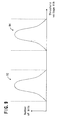
- Figure 2 is a graph showing the threshold voltage distribution of memory cell transistors.
- Figure 2 shows the distribution of threshold voltages Vth corresponding to a certain data value when electric charges are injected into the floating gate of a memory cell transistor so as to increase the threshold voltage Vth of the memory cell transistor to a prescribed level.
- the horizontal axis represents the threshold voltage Vth of a memory cell transistor
- the vertical axis represents the number of memory cell transistors indicating a threshold voltage Vth (i.e., the number of bits).
- the threshold voltages Vth of memory cell transistors vary to some extent (i.e., distribution).
- the threshold voltage is considered to have a certain range corresponding to a certain data value.
- the range is referred to as a threshold voltage range.
- Vth1 the maximum value (upper limit value) of the distribution range of threshold voltages Vth
- Vth2 the minimum value (lower limit value) thereof
- Vth3 1/2 x (Vth1 +Vth2).
- the threshold voltage Vth of the memory cell transistor is shifted toward a certain direction (a low voltage direction or a high voltage direction) over time. If the threshold voltage value is shifted into an adjacent threshold voltage range corresponding to another data value, data is read as a value different from the originally written data. Therefore, it is necessary to rewrite data (data refresh).
- the threshold voltage of a memory cell transistor is shifted to a lower level due to leakage of electric charges.
- data is rewritten into such a memory cell transistor.
- the determination section 2 compares the threshold voltage value of a memory cell transistor in the memory array 1 with a prescribed reference value to determine whether the threshold voltage value is higher or lower than the reference value.
- the reference value can be set to any value between the maximum and minimum values of a threshold voltage range corresponding to a written data value in the memory cell transistor.
- a middle value of a threshold voltage range is used as a reference value.
- the rewrite section 3 undergoes an electric charge reinjection operation for the charge accumulation layer of a memory cell transistor whose threshold voltage value is lower than the reference value to increase the threshold voltage value by a prescribed value.
- the prescribed value may be set to an arbitrary value.
- the prescribed value is set to a difference value between the maximum value and the middle value of the threshold voltage range.
- a write signal having a prescribed pulse width Tp is applied to the control voltage terminal (control gate) of a memory cell transistor.
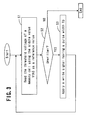
- Figure 3 is a flowchart showing a process of a rewrite operation according to Embodiment 1 of the present invention.
- step S1 the threshold voltage of a memory cell. (e.g., a memory cell transistor) is read out, where the middle value Vth3 of the threshold voltage range corresponding to a written data value in the memory cell is used as a reference value.
- the expression "a memory cell is read out” does not necessarily mean that the threshold voltage value of the memory cell is specified.
- step S2 it is determined whether or not the memory cell is in an unwritten state, based on the threshold voltage read out from the memory cell in step S1. Specifically, if the read threshold voltage value is lower than the middle value Vth3 of the threshold voltage range, the determination section 2 determines that the memory cell is in an unwritten state. The process goes to step S3 . If the read threshold voltage value is higher than or equal to the middle value Vth3 of the threshold voltage range, the determination section 2 determines that the memory cell is already in a written state. The process is ended.
- step S3 a write signal having a prescribed pulse width Tp is applied to the memory cell so that the threshold voltage value is increased by (Vth1 - Vth3).
- the threshold voltage value of the memory cell transistor falls within the range that is higher than or equal to the middle value Vth3 of the threshold voltage range and is lower than or equal to the maximum value Vthl. Therefore, the threshold voltage range after the rewrite operation is narrowed to about half compared to the threshold voltage range when data was originally written. In other words, a margin between two adjacent threshold voltage ranges is increased. Thus, the margin of data read is improved.
- the threshold voltage range of the memory cell transistor after the end of the data rewrite operation is present in a higher voltage region of the threshold voltage range when data was originally written . Therefore, even if electric charge leakage subsequently occurs in the charge accumulation layer, the time period during which the threshold voltage is maintained in the tolerable range (i.e., written threshold voltage range) is elongated. As a result, the data holding time is also elongated.
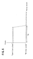
- Figure 4 is a flowchart showing a process of an operation for obtaining a pulse width of a write signal.
- step S11 the threshold voltage of each of a plurality of memory cells. (e.g., memory cell transistors) is set to the minimum voltage value Vth2 of the threshold voltage range.
- step S12 write signals having different pulse widths are applied to the plurality of memory cells.
- step S13 the threshold voltage of the plurality of memory cells are read out using the middle value Vth3 of the threshold voltage range as a reference value.
- step S14 the pulse width of the write signal applied to each memory cell is plotted on the horizontal axis, while the state of each memory cell which is determined by the determination section 2 ( Figure 1 ) based on the read threshold voltage is plotted on the vertical axis, to obtain a graph as shown in Figure 5 .
- Figure 5 is a graph for explaining a process of obtaining a pulse width of a write signal.
- a pulse width Tp at which "unwritten state” is changed to "written state” is a pulse width of the write signal to be obtained.
- the writesignal pulse width Tp may be measured, for example, when a production inspection is carried out before the shipment of non-volatile semiconductor memory devices, when an initial operation is carried out after the shipment of non-volatile semiconductor memory devices, when non-volatile semiconductor memory devices are powered ON, or the like.
- the non-volatile semiconductor memory devices can be used in a manner similar to typical flash memories. Also, by measuring the pulse width Tp of the write signal after the shipment of non-volatile semiconductor memory devices, a write time period optimal to practical conditions, such as a power source voltage, temperature, the characteristics of a memory cell over time, and the like, can be obtained.
- Embodiment 1 of the present invention is not limited to this, and is applicable to a memory cell transistor whose threshold voltage is shifted toward a higher voltage over time.
- a data rewrite operation may be carried out so that the threshold voltage value of a memory cell transistor is decreased by a prescribed value (e.g., Vth3 - Vth2) only if the threshold voltage value of a memory cell transistor is higher than a reference value (e.g., the middle value Vth3 ) .
- Embodiment 1 In the rewrite operation of Embodiment 1, application of a write signal is repeated under certain conditions. Therefore, a relatively long time is sometimes required for completion of a rewrite operation.
- Embodiment 2 of the present invention an example in which a data rewrite operation is completed in a shorter time will be described.
- Embodiment 2 a rewrite operation of the following type of memory cell will be described.
- data is read out from the memory cell immediately before the rewrite operation performed in Embodiment 2, the same data value as the value of written data is read out.
- data is read out from the memory cell after a certain time period, a data value different from the value of the written data may be read out due to the threshold voltage of a memory cell being shifted.
- Figure 6 is a flowchart showing a process of a rewrite operation according to Embodiment 2 of the present invention.
- step S21 the threshold voltage of a memory cell (e.g., a memory cell transistor) is read out, where the middle value Vth3 of a threshold voltage range corresponding to a written data value in the memory cell is used as a reference value.
- a memory cell e.g., a memory cell transistor
- step S22 it is determined whether or not the memory cell is in an unwritten state, based on the threshold voltage read out from the memory cell in step S21. Specifically, if the read threshold voltage value is lower than the middle value Vth3 of the threshold voltage range, the determination section 2 ( Figure 1 ) determines that the memory cell is in an unwritten state. The process goes to step S23. If the read threshold voltage value is higher than or equal to the middle value Vth3 of the threshold voltage range, the determination section 2 determines that the memory cell is already in a written state. The process is ended.
- the above-described steps are the same as steps S1 and S2 of Embodiment 1 ( Figure 3), respectively.
- step S23 a write signal having a prescribed pulse width Tp is applied to the memory cell once so that the threshold voltage value is increased by a prescribed value (Vth1 - Vth3: the half value of the threshold voltage range).
- Figure 7 is a graph showing the threshold voltage distribution of memory cell transistors.
- a determination value Vthr which is located at substantially the middle of a margin between adjacent threshold voltage ranges as shown in Figure 7, as a reference.
- the determination value Vthr indicates a determination voltage, which is used to determine a data value corresponding to the threshold voltage of a memory cell.
- the threshold voltage value of each memory cell is higher than at least the determination value Vthr.
- Embodiment 2 thus, by applying the write signal one time to increase the threshold voltage value of a memory cell by (Vth1 - Vth3), the threshold voltage value of the memory cell can be shifted into the written threshold voltage range.
- the lowest threshold voltage value of a memory cell is the same as the determination value Vthr.
- the threshold voltage value of the memory cell becomes higher than or equal to theminimum value Vth2 of the data written threshold voltage range.
- the threshold voltage value of the memory cell can be shifted into the data written threshold voltage range.
- a margin between two adjacent threshold voltage ranges is lower than one threshold voltage range. Inparticular, this is true formulti-valuememories . This is because in multi-value memories, there are a number of threshold voltage distributions corresponding to a number of data values in a prescribed power source voltage.
- the difference between the maximum value of the threshold voltage range of a memory cell and a reference value is higher than the difference value between the minimum value of the threshold voltage range of the memory cell and a determination value. This is because, particularly in multi-value memories, a margin between two adjacent threshold voltage ranges is typically lower than one threshold voltage range. This can be represented by expression (1). Vth1 - Vth3 > Vth2 - Vthr
- Vthr + (Vth1 - Vth3) Vth2
- the threshold voltage value of a memory cell is the same as the determination value Vthr, by increasing the threshold voltage value of the memory cell by (Vth1 - Vth3 ) , the threshold voltage value becomes higher than the minimum value Vth2 of the threshold voltage range.
- Embodiment 2 of the present invention is not limited to this, and is applicable to a memory cell transistor whose threshold voltage is shifted toward a higher voltage over time.
- Embodiment 3 a rewrite operation of the following type of memory cell will be described.
- data is read out from the memory cell immediately before the rewrite operation performed in Embodiment 3 , the same data value as the value of written data is read out.
- a data value different from the value of the written data may be read out due to the threshold voltage of a memory cell being shifted.
- Figure 8 is a flowchart showing a process of a rewrite operation according to Embodiment 3 of the present invention.
- step S31 the threshold voltage of a memory cell (e.g., a memory cell transistor) is read out, where the middle value Vth3 of a threshold voltage range corresponding to a written data value in the memory cell is used as a reference value.
- a memory cell e.g., a memory cell transistor
- step S32 it is determined whether or not the memory cell is in an unwritten state, based on the threshold voltage read out from the memory cell in step S31. Specifically, if the read threshold voltage value is lower than the middle value Vth3 of the threshold voltage range, the determination section 2 ( Figure 1 ) determines that the memory cell is in an unwritten state. The process goes to step S33. If the read threshold voltage value is higher than or equal to the middle value Vth3 of the threshold voltage range, the determination section 2 determines that the memory cell is already in a written state. The process is ended.
- the above-described steps are the same as steps S1 and S2 of Embodiment 1 ( Figure 3 ), respectively.
- step S33 a write signal having a prescribed pulse width Tp' is applied to the memory cell once so that the threshold voltage value is increased by a prescribed value (Vth2 - Vthr).
- a determination value Vthr which is located at substantially the middle of a margin between adjacent threshold voltage ranges as shown in Figure 7 , as a reference.
- the determination value Vthr indicates a determination voltage, which is used to determine a data value corresponding to the threshold voltage of a memory cell.
- the threshold voltage of a memory cell is higher than at least the determination value Vthr.
- Embodiment 3 of the present invention is not limited to this.
- Embodiment 3 in order to prevent a memory cell transistor from being shifted toward a higher voltage over time, data may be rewritten into such a memory cell transistor.
- a data rewrite operation may be carried out so that the threshold voltage value of a memory cell transistor is decreased by a prescribed value.
- the prescribed value is a difference value between the determination value (located at a substantially middle of a margin between one threshold voltage range and another threshold voltage range adjacent thereto on the higher voltage side) and the maximum value of the one threshold voltage range.
- the prescribed value is the determination value Vthr - Vth1.
- the memory array 1 comprises a plurality of memory cell transistors each having a charge accumulation layer.
- the threshold voltage of a memory cell transistor is regulated, so that one of two ormore data values is written into a memory cell transistor. It is determined whether the threshold voltage value of each memory cell transistor is higher or lower than a reference value, e.g., the middle value of the threshold voltage range corresponding to a written data value in the memory cell transistor. If the threshold voltage value is lower than the middle value, electric charges are reinjected again to the charge accumulation layer so that the threshold voltage value of the memory cell transistor is increased by the difference value (prescribed value) between the maximum value and middle value of the threshold voltage range.
- a change in threshold voltage can be compensated for in a shorter time.
- a margin between adjacent threshold voltage ranges can be enlarged and therefore the data holding property can be improved.
- a prescribed value for shifting the displaced threshold voltage of a memory cell transistor is set to: (1) the difference value between the maximum value of the threshold voltage range and the reference value; (2) the difference value between the minimum value of the threshold voltage range and the reference value; (3) the difference value between the minimum value of the threshold voltage range and a determination voltage for distinguishing the threshold voltage range from a lower threshold voltage range adjacent to the threshold voltage range; and (4) the difference value between the maximum value of the threshold voltage range and a determination voltage for distinguishing the threshold voltage range from a higher threshold voltage range adjacent to the threshold voltage range.
- the present invention is not limited to this.
- the prescribed value may be any value as long as it can enlarge a margin between two threshold voltage ranges corresponding to two data values. Even if a change in threshold voltage during the idle period is relatively small and the threshold voltage value of one memory cell is close to a reference value, the threshold voltage of the memory cell after a rewrite operation needs to be within the data written threshold voltage range. In this case, the same data as the written data can be read out.
- the present invention is not limited to such memory cells .
- the present invention is applicable to memory cells capable of storing a plurality of data values depending on voltage.
- a memory array in which by injecting electric charges into a charge accumulation layer, the threshold voltage of a memory cell transistor is regulated so that one value among two or more storable data values is written into the memory cell transistor.
- data is rewritten (reinjection of electric charges or redischarge of electric charges) so that the threshold voltage value is increased (or decreased) by a prescribed value and thus the threshold voltage is shifted to compensate for a change in threshold voltage, only if the threshold voltage, which has been shifted over time, is lower (or higher) than a prescribed reference value.
- the threshold voltage range can be narrowed so that the data holding property of a memory can be improved.
- a write signal having a prescribed pulse width is applied to a memory cell transistor requiring shift, once or a desired number of times, in order to shift the threshold voltage value by a prescribed value, a refresh operation can be quickly carried out.
Landscapes
- Engineering & Computer Science (AREA)
- Computer Hardware Design (AREA)
- Read Only Memory (AREA)
Abstract
Description
Claims (20)
- A non-volatile semiconductor memory device, comprising:a memory array comprising a plurality of memory cells, wherein each of the plurality of memory cells is capable of storing a plurality of data values depending on the voltages thereof, the plurality of data values include a first data value corresponding to a first voltage range and a second data value corresponding to a second voltage range, and the first data is written in one memory cell of the plurality of memory cells;a determination section for determining whether a voltage value of the one memory cell is higher or lower than a reference value set between a maximum value and a minimum value of the first voltage range; anda rewrite section for rewriting the first data into the one memory cell based on a determination result of the determination section so that a margin between the first voltage range and the second voltage range in the one memory cell is enlarged.
- A non-volatile semiconductor memory device according to claim 1, wherein the rewrite section shifts the voltage value of the one memory cell based on the determination result of the determination section so as to narrow the first voltage range.
- A non-volatile semiconductor memory device according to claim 2, wherein the rewrite section shifts the voltage value of the one memory cell by a prescribed value based on the determination result of the determination section.
- A non-volatile semiconductor memory device according to claim 3, wherein if the determination section determines that the voltage value of the one memory cell is lower than the reference value set between the maximum value and the minimum value of the first voltage range, the rewrite section increases the voltage value of the one memory cell by the prescribed value.
- A non-volatile semiconductor memory device according to claim 3, wherein if the determination section determines that the voltage value of the one memory cell is higher than the reference value set between the maximum value and the minimum value of the first voltage range, the rewrite section decreases the voltage value of the one memory cell by the prescribed value.
- A non-volatile semiconductor memory device according to claim 1, wherein the rewrite section shifts the voltage value of the one memory cell based on the determination result of the determination section so that the voltage value of the one memory cell is included in a range of the first voltage range on one side thereof relative to the reference value.
- A non-volatile semiconductor memory device according to claim 1, wherein:each of the plurality of memory cells is a memory cell transistor comprising a charge accumulation layer for accumulating electric charges; andthe memory cell transistor is capable of storing a plurality of data values depending on the amount of the electric charges accumulated in the charge accumulation layer.
- A non-volatile semiconductor memory device according to claim 1, wherein the rewrite section shifts the voltage value of the one memory cell by applying a write pulse signal having a prescribed pulse width to the one memory cell.
- A non-volatile semiconductor memory device according to claim 1, wherein the reference value is set to a middle value of the first voltage range.
- A non-volatile semiconductor memory device according to claim 3 , wherein the prescribed value is set to a difference value between the maximum value of the first voltage range and the reference value.
- A non-volatile semiconductor memory device according to claim 3 , wherein the prescribed value is set to a difference value between the minimum value of the first voltage range and the reference value.
- A non-volatile semiconductor memory device according to claim 3, wherein:the minimum value of the first voltage range is higher than a maximum value of the second voltage range; andthe prescribed value is set to a difference value between the minimum value of the first voltage range and a determination value indicating a determination voltage for distinguishing the first voltage range from the second voltage range.
- A non-volatile semiconductor memory device according to claim 12, wherein the determination value is set to a middle value between the first voltage range and the second voltage range.
- A non-volatile semiconductor memory device according to claim 3, wherein:the maximum value of the first voltage range is lower than a minimum value of the second voltage range; andthe prescribed value is set to a difference value between the maximum value of the first voltage range and a determination value indicating a determination voltage for distinguishing the first voltage range from the second voltage range.
- A non-volatile semiconductor memory device according to claim 14, wherein the determination value is set to a middle value between the first voltage range and the second voltage range.
- A rewriting method for a non-volatile semiconductor memory device, comprising the steps of:reading a voltage of a memory cell capable of storing a plurality of data values depending on the voltage thereof, wherein the plurality of data values include a first data value corresponding to a first voltage range and a second data value corresponding to a second voltage range, and the first data is written in the memory cell;determining whether a value of the voltage of the memory cell is higher or lower than a reference value set between a maximum value and a minimum value of the first voltage range; andrewriting the first data into the memory cell based on a determination result of the determining step so that a margin between the first voltage range and the second voltage range in the memory cell is enlarged.
- A rewriting method according to claim 16 , wherein the rewriting step comprises shifting the voltage value of the memory cell so that the voltage value of the memory cell is higher than the reference value if the determining step determines that the voltage value of the memory cell is smaller than the reference value set between the maximum value and the minimum value of the first voltage range.
- A rewriting method according to claim 16, wherein the rewriting step comprises shifting the voltage value of the memory cell so that the voltage value of the memory cell is smaller than the reference value if the determining step determines that the voltage value of the memory cell is higher than the reference value set between the maximum value and the minimum value of the first voltage range.
- A rewriting method according to claim 16, wherein:the memory cell is a memory cell transistor comprising a charge accumulation layer for accumulating electric charges; andthe rewriting step comprises reinjecting electric charges into the charge accumulation layer.
- A rewriting method according to claim 16, wherein the rewriting step comprises shifting the voltage value of the memory cell by applying a write signal having a prescribed pulse width to the memory cell.
Applications Claiming Priority (2)
| Application Number | Priority Date | Filing Date | Title |
|---|---|---|---|
| JP2002261921A JP2004103089A (en) | 2002-09-06 | 2002-09-06 | Nonvolatile semiconductor memory device and rewriting method thereof |
| JP2002261921 | 2002-09-06 |
Publications (2)
| Publication Number | Publication Date |
|---|---|
| EP1396862A1 true EP1396862A1 (en) | 2004-03-10 |
| EP1396862B1 EP1396862B1 (en) | 2008-01-16 |
Family
ID=31712349
Family Applications (1)
| Application Number | Title | Priority Date | Filing Date |
|---|---|---|---|
| EP03020113A Expired - Lifetime EP1396862B1 (en) | 2002-09-06 | 2003-09-04 | Non-volatile semiconductor memory device and rewriting method |
Country Status (7)
| Country | Link |
|---|---|
| US (1) | US6816409B2 (en) |
| EP (1) | EP1396862B1 (en) |
| JP (1) | JP2004103089A (en) |
| KR (1) | KR100632791B1 (en) |
| CN (1) | CN100380523C (en) |
| DE (1) | DE60318659T2 (en) |
| TW (1) | TWI297498B (en) |
Families Citing this family (35)
| Publication number | Priority date | Publication date | Assignee | Title |
|---|---|---|---|---|
| US6751766B2 (en) | 2002-05-20 | 2004-06-15 | Sandisk Corporation | Increasing the effectiveness of error correction codes and operating multi-level memory systems by using information about the quality of the stored data |
| JP4124692B2 (en) * | 2003-04-25 | 2008-07-23 | シャープ株式会社 | Nonvolatile semiconductor memory device |
| US7372731B2 (en) * | 2003-06-17 | 2008-05-13 | Sandisk Il Ltd. | Flash memories with adaptive reference voltages |
| CN100543875C (en) * | 2004-09-01 | 2009-09-23 | 旺宏电子股份有限公司 | Programming method of nonvolatile memory |
| US7092290B2 (en) * | 2004-11-16 | 2006-08-15 | Sandisk Corporation | High speed programming system with reduced over programming |
| WO2007043133A1 (en) * | 2005-10-04 | 2007-04-19 | Spansion Llc | Semiconductor device and method for controlling same |
| JP2007149241A (en) * | 2005-11-29 | 2007-06-14 | Matsushita Electric Ind Co Ltd | Nonvolatile semiconductor memory device |
| JP2007193867A (en) * | 2006-01-17 | 2007-08-02 | Matsushita Electric Ind Co Ltd | Nonvolatile semiconductor memory device and rewriting method thereof |
| KR100888695B1 (en) | 2007-02-27 | 2009-03-16 | 삼성전자주식회사 | Flash memory device performing oversampling read operation and its data reading method |
| US7577036B2 (en) | 2007-05-02 | 2009-08-18 | Micron Technology, Inc. | Non-volatile multilevel memory cells with data read of reference cells |
| KR100888842B1 (en) * | 2007-06-28 | 2009-03-17 | 삼성전자주식회사 | Flash memory device that can optimize the read voltage and how to set its read voltage |
| US8938655B2 (en) * | 2007-12-20 | 2015-01-20 | Spansion Llc | Extending flash memory data retension via rewrite refresh |
| JP5197241B2 (en) * | 2008-09-01 | 2013-05-15 | ルネサスエレクトロニクス株式会社 | Semiconductor device |
| KR101572830B1 (en) | 2009-06-22 | 2015-11-30 | 삼성전자주식회사 | Method of programming non-volatile memory device, non-volatile memory device and non-volatile memory system |
| US7944744B2 (en) * | 2009-06-30 | 2011-05-17 | Sandisk Il Ltd. | Estimating values related to discharge of charge-storing memory cells |
| KR20110050923A (en) * | 2009-11-09 | 2011-05-17 | 삼성전자주식회사 | Semiconductor memory device, semiconductor memory module and semiconductor memory system having same |
| KR101618311B1 (en) * | 2010-02-08 | 2016-05-04 | 삼성전자주식회사 | Flash memory device and reading method thereof |
| JP2013137848A (en) * | 2011-12-28 | 2013-07-11 | Univ Of Tokyo | Memory controller, flash memory system, and method for controlling flash memory |
| US8645770B2 (en) * | 2012-01-18 | 2014-02-04 | Apple Inc. | Systems and methods for proactively refreshing nonvolatile memory |
| US9183940B2 (en) | 2013-05-21 | 2015-11-10 | Aplus Flash Technology, Inc. | Low disturbance, power-consumption, and latency in NAND read and program-verify operations |
| US9263137B2 (en) | 2013-06-27 | 2016-02-16 | Aplus Flash Technology, Inc. | NAND array architecture for multiple simutaneous program and read |
| WO2015013689A2 (en) | 2013-07-25 | 2015-01-29 | Aplus Flash Technology, Inc. | Nand array hiarchical bl structures for multiple-wl and all -bl simultaneous erase, erase-verify, program, program-verify, and read operations |
| US9293205B2 (en) | 2013-09-14 | 2016-03-22 | Aplus Flash Technology, Inc | Multi-task concurrent/pipeline NAND operations on all planes |
| CN104681089A (en) * | 2013-11-26 | 2015-06-03 | 旺宏电子股份有限公司 | Method, electronic device and controller for restoring an array of multiple storage units |
| US9613704B2 (en) | 2013-12-25 | 2017-04-04 | Aplus Flash Technology, Inc | 2D/3D NAND memory array with bit-line hierarchical structure for multi-page concurrent SLC/MLC program and program-verify |
| CN104751893B (en) * | 2013-12-30 | 2018-09-07 | 北京兆易创新科技股份有限公司 | Enhance the method for NOR type FLASH reliabilities |
| CN104751898B (en) * | 2013-12-30 | 2018-04-24 | 北京兆易创新科技股份有限公司 | The method of NOR type FLASH data recoveries |
| US9659636B2 (en) | 2014-07-22 | 2017-05-23 | Peter Wung Lee | NAND memory array with BL-hierarchical structure for concurrent all-BL, all-threshold-state program, and alternative-WL program, odd/even read and verify operations |
| KR102190241B1 (en) * | 2014-07-31 | 2020-12-14 | 삼성전자주식회사 | Operating mehtod of memory controller and nonvolatile memory device |
| US9728278B2 (en) | 2014-10-24 | 2017-08-08 | Micron Technology, Inc. | Threshold voltage margin analysis |
| CN106920567A (en) * | 2015-12-24 | 2017-07-04 | 北京兆易创新科技股份有限公司 | The method for refreshing and device of a kind of memory |
| JP2018045742A (en) * | 2016-09-13 | 2018-03-22 | ルネサスエレクトロニクス株式会社 | Storage device and management method for storage device |
| JP6997595B2 (en) * | 2017-11-09 | 2022-01-17 | ルネサスエレクトロニクス株式会社 | Semiconductor storage device and control method for semiconductor storage device |
| WO2021223075A1 (en) | 2020-05-06 | 2021-11-11 | Yangtze Memory Technologies Co., Ltd. | Non-volatile memory device and control method thereof |
| US11929127B2 (en) * | 2021-08-31 | 2024-03-12 | Micron Technology, Inc. | Selective data pattern write scrub for a memory system |
Citations (5)
| Publication number | Priority date | Publication date | Assignee | Title |
|---|---|---|---|---|
| US5768193A (en) * | 1996-06-17 | 1998-06-16 | Aplus Integrated Circuits, Inc. | Bit-refreshable method and circuit for refreshing a nonvolatile flash memory |
| US5818762A (en) * | 1995-07-19 | 1998-10-06 | Sony Corporation | Memory having charge-carrying floating gate memory cells with time/voltage dependent refresh |
| EP0911833A2 (en) * | 1997-09-08 | 1999-04-28 | Invox Technology | Multi-level non-volatile memory with error detection and correction |
| US6195287B1 (en) * | 1999-02-03 | 2001-02-27 | Sharp Kabushiki Kaisha | Data programming method for a nonvolatile semiconductor storage |
| EP1182669A2 (en) * | 2000-08-23 | 2002-02-27 | Sharp Kabushiki Kaisha | Non-volatile semiconductor memory device |
Family Cites Families (7)
| Publication number | Priority date | Publication date | Assignee | Title |
|---|---|---|---|---|
| JP3584607B2 (en) | 1996-05-10 | 2004-11-04 | ソニー株式会社 | Non-volatile storage device |
| US5738193A (en) | 1996-07-19 | 1998-04-14 | General Motors Corporation | Roller clutch with snap fit roller control cars |
| US6134148A (en) * | 1997-09-30 | 2000-10-17 | Hitachi, Ltd. | Semiconductor integrated circuit and data processing system |
| US6018477A (en) * | 1998-10-08 | 2000-01-25 | Information Storage Devices, Inc. | Intelligent refreshing method and apparatus for increasing multi-level non-volatile memory charge retention reliability |
| US6314026B1 (en) * | 1999-02-08 | 2001-11-06 | Kabushiki Kaisha Toshiba | Nonvolatile semiconductor device using local self boost technique |
| JP3569185B2 (en) * | 1999-12-24 | 2004-09-22 | Necエレクトロニクス株式会社 | Nonvolatile semiconductor memory device |
| US6343033B1 (en) * | 2000-02-25 | 2002-01-29 | Advanced Micro Devices, Inc. | Variable pulse width memory programming |
-
2002
- 2002-09-06 JP JP2002261921A patent/JP2004103089A/en active Pending
-
2003
- 2003-09-03 US US10/654,674 patent/US6816409B2/en not_active Expired - Fee Related
- 2003-09-04 EP EP03020113A patent/EP1396862B1/en not_active Expired - Lifetime
- 2003-09-04 DE DE60318659T patent/DE60318659T2/en not_active Expired - Lifetime
- 2003-09-05 CN CNB031566855A patent/CN100380523C/en not_active Expired - Fee Related
- 2003-09-05 TW TW092124637A patent/TWI297498B/en not_active IP Right Cessation
- 2003-09-06 KR KR1020030062403A patent/KR100632791B1/en not_active Expired - Fee Related
Patent Citations (5)
| Publication number | Priority date | Publication date | Assignee | Title |
|---|---|---|---|---|
| US5818762A (en) * | 1995-07-19 | 1998-10-06 | Sony Corporation | Memory having charge-carrying floating gate memory cells with time/voltage dependent refresh |
| US5768193A (en) * | 1996-06-17 | 1998-06-16 | Aplus Integrated Circuits, Inc. | Bit-refreshable method and circuit for refreshing a nonvolatile flash memory |
| EP0911833A2 (en) * | 1997-09-08 | 1999-04-28 | Invox Technology | Multi-level non-volatile memory with error detection and correction |
| US6195287B1 (en) * | 1999-02-03 | 2001-02-27 | Sharp Kabushiki Kaisha | Data programming method for a nonvolatile semiconductor storage |
| EP1182669A2 (en) * | 2000-08-23 | 2002-02-27 | Sharp Kabushiki Kaisha | Non-volatile semiconductor memory device |
Also Published As
| Publication number | Publication date |
|---|---|
| DE60318659T2 (en) | 2009-01-15 |
| EP1396862B1 (en) | 2008-01-16 |
| US6816409B2 (en) | 2004-11-09 |
| KR100632791B1 (en) | 2006-10-11 |
| US20040071023A1 (en) | 2004-04-15 |
| CN100380523C (en) | 2008-04-09 |
| KR20040022409A (en) | 2004-03-12 |
| DE60318659D1 (en) | 2008-03-06 |
| CN1492446A (en) | 2004-04-28 |
| TWI297498B (en) | 2008-06-01 |
| JP2004103089A (en) | 2004-04-02 |
| TW200414200A (en) | 2004-08-01 |
Similar Documents
| Publication | Publication Date | Title |
|---|---|---|
| US6816409B2 (en) | Non-volatile semiconductor memory device and rewriting method | |
| KR101148303B1 (en) | Charge loss compensation during programming of a memory device | |
| US8027202B2 (en) | Method of programming a flash memory device using self boosting | |
| KR100906525B1 (en) | Semiconductor integrated circuit de?ce | |
| US8526239B2 (en) | Semiconductor memory device and method of operating the same | |
| KR100683856B1 (en) | Programming method of flash memory to compensate for reduction of read margin due to high temperature stress | |
| US8411501B2 (en) | Programming method for non-volatile memory device | |
| TWI385664B (en) | Hybrid programming methods for non-volatile memory storage elements | |
| US6839279B2 (en) | Nonvolatile semiconductor memory device | |
| JP2000222893A (en) | Method of writing information to nonvolatile semiconductor memory device | |
| JP2011258289A (en) | Method for detecting threshold value of memory cell | |
| KR20030096307A (en) | Soft program and soft program verify of the core cells in flash memory array | |
| JP2011028827A (en) | Semiconductor memory device | |
| US5818762A (en) | Memory having charge-carrying floating gate memory cells with time/voltage dependent refresh | |
| CN101015020A (en) | Method of improving erase voltage distribution for a flash memory array having dummy wordlines | |
| CN101236786B (en) | Method for programming multi-level memory cell memory array | |
| US7447076B2 (en) | Systems for reverse reading in non-volatile memory with compensation for coupling | |
| KR100629193B1 (en) | Nonvolatile semiconductor memory device and recording method thereof | |
| KR101402230B1 (en) | Non-volatile memory device having dummy cell and program method thereof | |
| KR100769258B1 (en) | Nonvolatile Memory Devices Can Reduce Threshold Voltage Distributions | |
| KR20100117906A (en) | Nonvolatile memory device and method of operating the same | |
| JP2005044454A (en) | Semiconductor memory device and drive control method for semiconductor memory device | |
| KR100840562B1 (en) | Nonvolatile Semiconductor Memory and Recording Method | |
| JPWO2002067267A1 (en) | Multi-level nonvolatile semiconductor memory device | |
| US7596020B2 (en) | Multi-level nonvolatile semiconductor memory device capable of discretely controlling a charge storage layer potential based upon accumulated electrons |
Legal Events
| Date | Code | Title | Description |
|---|---|---|---|
| PUAI | Public reference made under article 153(3) epc to a published international application that has entered the european phase |
Free format text: ORIGINAL CODE: 0009012 |
|
| AK | Designated contracting states |
Kind code of ref document: A1 Designated state(s): AT BE BG CH CY CZ DE DK EE ES FI FR GB GR HU IE IT LI LU MC NL PT RO SE SI SK TR |
|
| AX | Request for extension of the european patent |
Extension state: AL LT LV MK |
|
| 17P | Request for examination filed |
Effective date: 20040903 |
|
| AKX | Designation fees paid |
Designated state(s): DE FR IT |
|
| 17Q | First examination report despatched |
Effective date: 20050113 |
|
| GRAC | Information related to communication of intention to grant a patent modified |
Free format text: ORIGINAL CODE: EPIDOSCIGR1 |
|
| GRAJ | Information related to disapproval of communication of intention to grant by the applicant or resumption of examination proceedings by the epo deleted |
Free format text: ORIGINAL CODE: EPIDOSDIGR1 |
|
| GRAP | Despatch of communication of intention to grant a patent |
Free format text: ORIGINAL CODE: EPIDOSNIGR1 |
|
| RIN1 | Information on inventor provided before grant (corrected) |
Inventor name: TANAKA, HIDEHIKO |
|
| GRAS | Grant fee paid |
Free format text: ORIGINAL CODE: EPIDOSNIGR3 |
|
| GRAA | (expected) grant |
Free format text: ORIGINAL CODE: 0009210 |
|
| AK | Designated contracting states |
Kind code of ref document: B1 Designated state(s): DE FR IT |
|
| REF | Corresponds to: |
Ref document number: 60318659 Country of ref document: DE Date of ref document: 20080306 Kind code of ref document: P |
|
| ET | Fr: translation filed | ||
| PLBE | No opposition filed within time limit |
Free format text: ORIGINAL CODE: 0009261 |
|
| STAA | Information on the status of an ep patent application or granted ep patent |
Free format text: STATUS: NO OPPOSITION FILED WITHIN TIME LIMIT |
|
| 26N | No opposition filed |
Effective date: 20081017 |
|
| PGFP | Annual fee paid to national office [announced via postgrant information from national office to epo] |
Ref country code: FR Payment date: 20120926 Year of fee payment: 10 Ref country code: DE Payment date: 20120829 Year of fee payment: 10 Ref country code: IT Payment date: 20120915 Year of fee payment: 10 |
|
| REG | Reference to a national code |
Ref country code: DE Ref legal event code: R119 Ref document number: 60318659 Country of ref document: DE Effective date: 20140401 |
|
| REG | Reference to a national code |
Ref country code: FR Ref legal event code: ST Effective date: 20140530 |
|
| PG25 | Lapsed in a contracting state [announced via postgrant information from national office to epo] |
Ref country code: DE Free format text: LAPSE BECAUSE OF NON-PAYMENT OF DUE FEES Effective date: 20140401 Ref country code: FR Free format text: LAPSE BECAUSE OF NON-PAYMENT OF DUE FEES Effective date: 20130930 Ref country code: IT Free format text: LAPSE BECAUSE OF NON-PAYMENT OF DUE FEES Effective date: 20130904 |