EP1391928A2 - Chipanordung mit zumindest zwei Halbleiterchips und Verfahren zur Überprüfung der Ausrichtung zweier benachbarter Halbleiterchips - Google Patents
Chipanordung mit zumindest zwei Halbleiterchips und Verfahren zur Überprüfung der Ausrichtung zweier benachbarter Halbleiterchips Download PDFInfo
- Publication number
- EP1391928A2 EP1391928A2 EP03017866A EP03017866A EP1391928A2 EP 1391928 A2 EP1391928 A2 EP 1391928A2 EP 03017866 A EP03017866 A EP 03017866A EP 03017866 A EP03017866 A EP 03017866A EP 1391928 A2 EP1391928 A2 EP 1391928A2
- Authority
- EP
- European Patent Office
- Prior art keywords
- chip
- semiconductor chips
- semiconductor chip
- determined
- semiconductor
- Prior art date
- Legal status (The legal status is an assumption and is not a legal conclusion. Google has not performed a legal analysis and makes no representation as to the accuracy of the status listed.)
- Granted
Links
Images


Classifications
-
- H—ELECTRICITY
- H10—SEMICONDUCTOR DEVICES; ELECTRIC SOLID-STATE DEVICES NOT OTHERWISE PROVIDED FOR
- H10P—GENERIC PROCESSES OR APPARATUS FOR THE MANUFACTURE OR TREATMENT OF DEVICES COVERED BY CLASS H10
- H10P74/00—Testing or measuring during manufacture or treatment of wafers, substrates or devices
- H10P74/27—Structural arrangements therefor
- H10P74/277—Circuits for electrically characterising or monitoring manufacturing processes, e.g. circuits in tested chips or circuits in testing wafers
-
- H—ELECTRICITY
- H10—SEMICONDUCTOR DEVICES; ELECTRIC SOLID-STATE DEVICES NOT OTHERWISE PROVIDED FOR
- H10W—GENERIC PACKAGES, INTERCONNECTIONS, CONNECTORS OR OTHER CONSTRUCTIONAL DETAILS OF DEVICES COVERED BY CLASS H10
- H10W42/00—Arrangements for protection of devices
- H10W42/40—Arrangements for protection of devices protecting against tampering, e.g. unauthorised inspection or reverse engineering
- H10W42/405—Arrangements for protection of devices protecting against tampering, e.g. unauthorised inspection or reverse engineering using active circuits
-
- H—ELECTRICITY
- H10—SEMICONDUCTOR DEVICES; ELECTRIC SOLID-STATE DEVICES NOT OTHERWISE PROVIDED FOR
- H10W—GENERIC PACKAGES, INTERCONNECTIONS, CONNECTORS OR OTHER CONSTRUCTIONAL DETAILS OF DEVICES COVERED BY CLASS H10
- H10W90/00—Package configurations
-
- H—ELECTRICITY
- H10—SEMICONDUCTOR DEVICES; ELECTRIC SOLID-STATE DEVICES NOT OTHERWISE PROVIDED FOR
- H10W—GENERIC PACKAGES, INTERCONNECTIONS, CONNECTORS OR OTHER CONSTRUCTIONAL DETAILS OF DEVICES COVERED BY CLASS H10
- H10W46/00—Marks applied to devices, e.g. for alignment or identification
-
- H—ELECTRICITY
- H10—SEMICONDUCTOR DEVICES; ELECTRIC SOLID-STATE DEVICES NOT OTHERWISE PROVIDED FOR
- H10W—GENERIC PACKAGES, INTERCONNECTIONS, CONNECTORS OR OTHER CONSTRUCTIONAL DETAILS OF DEVICES COVERED BY CLASS H10
- H10W72/00—Interconnections or connectors in packages
-
- H—ELECTRICITY
- H10—SEMICONDUCTOR DEVICES; ELECTRIC SOLID-STATE DEVICES NOT OTHERWISE PROVIDED FOR
- H10W—GENERIC PACKAGES, INTERCONNECTIONS, CONNECTORS OR OTHER CONSTRUCTIONAL DETAILS OF DEVICES COVERED BY CLASS H10
- H10W72/00—Interconnections or connectors in packages
- H10W72/071—Connecting or disconnecting
- H10W72/072—Connecting or disconnecting of bump connectors
- H10W72/07221—Aligning
- H10W72/07223—Active alignment, e.g. using optical alignment using marks or sensors
-
- H—ELECTRICITY
- H10—SEMICONDUCTOR DEVICES; ELECTRIC SOLID-STATE DEVICES NOT OTHERWISE PROVIDED FOR
- H10W—GENERIC PACKAGES, INTERCONNECTIONS, CONNECTORS OR OTHER CONSTRUCTIONAL DETAILS OF DEVICES COVERED BY CLASS H10
- H10W72/00—Interconnections or connectors in packages
- H10W72/071—Connecting or disconnecting
- H10W72/072—Connecting or disconnecting of bump connectors
- H10W72/07231—Techniques
- H10W72/07236—Soldering or alloying
-
- H—ELECTRICITY
- H10—SEMICONDUCTOR DEVICES; ELECTRIC SOLID-STATE DEVICES NOT OTHERWISE PROVIDED FOR
- H10W—GENERIC PACKAGES, INTERCONNECTIONS, CONNECTORS OR OTHER CONSTRUCTIONAL DETAILS OF DEVICES COVERED BY CLASS H10
- H10W90/00—Package configurations
- H10W90/20—Configurations of stacked chips
- H10W90/284—Configurations of stacked chips characterised by structural arrangements for measuring or testing
-
- H—ELECTRICITY
- H10—SEMICONDUCTOR DEVICES; ELECTRIC SOLID-STATE DEVICES NOT OTHERWISE PROVIDED FOR
- H10W—GENERIC PACKAGES, INTERCONNECTIONS, CONNECTORS OR OTHER CONSTRUCTIONAL DETAILS OF DEVICES COVERED BY CLASS H10
- H10W90/00—Package configurations
- H10W90/701—Package configurations characterised by the relative positions of pads or connectors relative to package parts
- H10W90/721—Package configurations characterised by the relative positions of pads or connectors relative to package parts of bump connectors
- H10W90/722—Package configurations characterised by the relative positions of pads or connectors relative to package parts of bump connectors between stacked chips
Definitions
- the invention relates to a semiconductor chip, a chip arrangement with at least two semiconductor chips and a method for Check the alignment of two stacked semiconductor chips in such a chip arrangement according to the sibling Claims.
- such are also to be protected Semiconductor chips applied to a carrier, so that the active Area of the semiconductor chip that contains the information to be protected has load-bearing integrated circuit, from one Carrier is covered.
- the chip is not detachable from this carrier and again can be placed identically without changing the degree of coverage.
- Advantageous embodiments of the invention are in the subordinate ones Claims specified. It is advantageous here if an originally initialized value is stored on the chip and at certain times with that actually determinable value is compared.
- the value of the coverage is for example via a resistance measurement, but also by means of capacitive or corresponding measurements possible.
- connection surface or the opposite surface producing a cover the carrier or another chip in a chip arrangement has such a shape that even minimal deviations significantly measurable from an original cover are. This can be done, for example, with slanted figures or curved edges.
- a first semiconductor chip 1 is shown, the consists of a substrate S and an active layer 5.
- this active layer is a more or less complex integrated one Circuit included, at least part of this integrated circuit the circuit arrangement shown in Figure 3 having.
- the first semiconductor chip 1 is a second semiconductor chip arranged, the two chips in the direction of Arrows shown on the right are joined together so that the Pads 3 of the first semiconductor chip 1 with the pads 4 of the second semiconductor chip 2 merged overlapping are.
- FIG. 2 Such an offset is shown by way of example in FIG. 2.
- the pad has 4 of the second semiconductor chip also has a triangular shape on, as shown in dashed lines, where if it is an isosceles triangle, the tip on the base B of the respective other triangle.
- FIG. 2 It can be seen from FIG. 2 that it already has a connecting surface an offset can be determined. On closer inspection it is easy to see, however, that if there is an offset in two directions the extent of overlap at least within certain limits of the offset can remain the same. For this reason, it is advantageous if, as in FIG. 2 is shown, two pads are provided on the chip are that are not aligned identically. According to FIG. 2 the base B of the triangle in section b is 90 degrees opposite base B rotated in cutout a.
- the overlap can now be carried out with a measuring circuit such as that is shown in Figure 3 can be determined.
- a measuring circuit such as that is shown in Figure 3 can be determined.
- the pad 3 With the pad 3 is connected to a measuring device 6, the one Resistance measurement takes place when a conductive connection between the pad 3 and an opposite in Overlapped area is present.
- the measuring device 6 has a capacitance value determined if there is no conductive connection.
- a processing device 8 provided in the embodiment shown in Figure 3 is a processing device 8 provided. This reads after a first assembly of the semiconductor chip in a chip arrangement or on a carrier the measured with the measuring device and from an overlap and stores it in a Storage device 7. During the further operation of the Semiconductor chips 1, for example each time it is started up again or even during ongoing operations from the measuring device 6 again the one corresponding to an overlap Value read out from the processing device and with the value stored in the storage device 7 compared. If these two values are not identical, then must the overlap on the pad 3 have changed. This can only be done in that the semiconductor chip was separated from its carrier.
- carrier means on the one hand that it is an identical or similar semiconductor chip or a other carrier material, which has an area which corresponds to the Pad 3 of the semiconductor chip brought into overlap was and a significant change in the event of an offset of the overlap.
- connection surface 3 This is diamond-shaped overlapped a pad 4 '.
- an offset of the semiconductor chip relative to its carrier to a constant overlap within certain limits can lead.
- faces the opposite surface Form 4 it can be seen that there is already a shift minimal form in one of the directions to a unique Change in the value of the overlap leads.
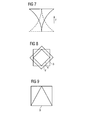
- 5, 6, 7 and 9 are further embodiments of the pad 3 and 4 respectively. These can also be combined with one another as can be seen, for example, in FIG. 9 is.
- connection surfaces lead to a change in the overlap value that is non-linear to offset.
- FIG. 4 Another embodiment of a chip arrangement is shown in Figure 4 shown.
- Two semiconductor chips 2 are located here and 2 'side by side, the first semiconductor chip 1 both Semiconductor chips interconnected. It's easy to see that moreover by combining the illustrated Exemplary embodiments by supplementing and multiplying individual ones Elements possible while maintaining the inventive concept is.
- the stored value that corresponds to the overlap usable as a so-called watermark. This means, it can be used as an individual indicator or as Basis for the generation of a key for data exchange to be used outside the arrangement.
- the invention can also be used for quality controls be used.
- the arrangement can be done by Comparison with one previously stored on at least one of the chips predetermined value determine whether the alignment of the chip with respect to the carrier is sufficiently precise. Lies the value outside of predetermined limits, so it is possible that the order automatically refuses to operate.
- that originally in the storage device can also stored value when manufacturing from outside be checked and used for quality control.
Landscapes
- Semiconductor Integrated Circuits (AREA)
- Wire Bonding (AREA)
Abstract
Description
- Figur 1
- eine Chipanordnung,
- Figur 2
- ein Ausführungsbeispiel von Anschlußflächen mit unterschiedlichen Abdeckungsgraden
- Figur 3
- eine Schaltungsanordnung zur Bestimmung des Abdeckungsgrades,
- Figur 4
- ein weiteres Ausführungsbeispiel einer Chipanordnung,
- Figur 5
- ein weiteres Ausführungsbeispiel einer Anschlußfläche,
- Figur 6
- ein weiteres Ausführungsbeispiel einer Anschlußfläche,
- Figur 7
- noch ein weiteres Ausführungsbeispiel zweier gegenüberliegender Anschlußflächen
- Figur 8
- ein weiteres Ausführungsbeispiel einer Anschlußfläche
- Figur 9
- noch ein Ausführungsbeispiel einer Anschlußfläche.
- 1
- erster Chip
- 2
- zweiter Chip
- S
- Substrat
- 3
- Anschlußfläche, Pad
- 4
- Anschlußfläche, Pad
- 5
- aktive Schicht
- 6
- Meßeinrichtung
- 7
- Speichereinrichtung
- 8
- Verarbeitungseinrichtung, Vergleichseinrichtung
Claims (15)
- Halbleiterchip mit einer aktiven Schicht (5), die von einem Substrat(S) getragen wird und zumindest einer Anschlußfläche (3), wobei die aktive Schicht (5) eine Detektoreinrichtung (6,7,8) aufweist, mit der ein Abdeckungsgrad der zumindest einen Anschlußfläche (3), bestimmbar ist.
- Halbleiterchip nach Anspruch 1, bei dem
die Detektoreinrichtung mittels einer Meßeinrichtung 6 einen Abdeckungsgrad der zumindest einen Anschlußfläche (3) bestimmt und mittels einer Vergleichseinrichtung (8) mit einem in einer Speichereinrichtung (7) gespeicherten vorgestimmten Wert vergleicht. - Halbleiterchip nach Anspruch 1, bei dem
die Anschlußfläche eine nichtquadratische Form aufweist. - Halbleiterchip nach Anspruch 3, bei dem
die Anschlußfläche (3) dreieckförmig ist. - Halbleiterchip nach Anspruch 3, bei dem
die Anschlußfläche (3) rautenförmig ist. - Halbleiterchip nach Anspruch 4, bei dem
zumindest zwei Anschlußflächen (3) als gleichschenklige Dreiecke vorgesehen sind, deren jeweilige Basen (b) zueinander nicht parallel ausgerichtet sind. - Halbleiterchip nach Anspruch 1, bei dem
das Abdeckungsausmaß mittels Widerstandsmessung feststellbar ist. - Halbleiterchip nach Anspruch 1, bei dem das Abdeckungsausmaß mittels Kapazitätsmessung feststellbar ist.
- Halbleiterchip nach Anspruch 1, bei dem die
Anschlußfläche (3) zum zusätzlichen Übertragen von Daten und/oder Energie vorgesehen ist. - Chipanordnung mit zumindest zwei Halbleiterchips (1,2) wobei zumindest einer der zumindest zwei Halbleiterchips nach einem der Patentansprüche 1 bis 8 ausgebildet ist, dessen Anschlußfläche (3) auf dem anderen Chip (2) einer Anschlußfläche (4) gegenübersteht, die sich zumindest teilweise überlappen.
- Chipanordnung nach Anspruch 10, wobei
die zumindest zwei Halbleiterchips (1,2) nach einem der Patentansprüche 1 bis 8 ausgebildet sind. - Verfahren zum Überprüfen der Ausrichtung zumindest zweier übereinanderliegender Halbleiterchips in einer Chipanordnung gemäß Patentanspruch 10 oder 11, wobei das Ausmaß der gegenseitigen Ausrichtung der zumindest zwei Halbleiterchips (1, 2) zueinander durch ein Bestimmen des Überlappungsausmaßes der gegenüberliegenden Anschlußflächen (3,4) ermittelt wird.
- Verfahren nach Anspruch 12, bei dem
der Wert der Überlappung der gegenüberliegenden Anschlußflächen mit einem abgespeicherten Wert verglichen wird. - Verfahren nach Anspruch 13, bei dem
in einem der zumindest zwei Halbleiterchips ein Signal erzeugt wird, wenn eine Abweichung zwischen dem ermittelten Wert und dem vorbestimmten Wert feststellbar ist. - Verfahren nach Anspruch 14, bei dem
bei der ersten Inbetriebnahme der Chipanordnung das Ausmaß der Überlappung der Anschlußflächen bestimmt wird und als vorbestimmter Wert in zumindest einem der zumindest zwei Halbleiterchips abgespeichert wird.
Applications Claiming Priority (2)
| Application Number | Priority Date | Filing Date | Title |
|---|---|---|---|
| DE10238835A DE10238835A1 (de) | 2002-08-23 | 2002-08-23 | Halbleiterchip, Chipanordnung mit zumindest zwei Halbleiterchips und Verfahren zur Überprüfung der Ausrichtung zumindest zweier übereinander liegender Halbleiterchips in einer Chipanordnung |
| DE10238835 | 2002-08-23 |
Publications (3)
| Publication Number | Publication Date |
|---|---|
| EP1391928A2 true EP1391928A2 (de) | 2004-02-25 |
| EP1391928A3 EP1391928A3 (de) | 2006-03-15 |
| EP1391928B1 EP1391928B1 (de) | 2009-03-18 |
Family
ID=30775548
Family Applications (1)
| Application Number | Title | Priority Date | Filing Date |
|---|---|---|---|
| EP03017866A Expired - Lifetime EP1391928B1 (de) | 2002-08-23 | 2003-08-05 | Chipanordung mit zumindest zwei Halbleiterchips und Verfahren zur Überprüfung der Ausrichtung zweier benachbarter Halbleiterchips |
Country Status (2)
| Country | Link |
|---|---|
| EP (1) | EP1391928B1 (de) |
| DE (2) | DE10238835A1 (de) |
Cited By (2)
| Publication number | Priority date | Publication date | Assignee | Title |
|---|---|---|---|---|
| EP1587141A3 (de) * | 2004-04-13 | 2007-12-05 | Sun Microsystems, Inc. | Methode und Apparat zur kapazitivgekoppelten Kommunikation innerhalb eines Chipstapels |
| EP2615641A3 (de) * | 2006-01-24 | 2014-06-04 | Nds Limited | Chip-Attacken-Schutz |
Family Cites Families (9)
| Publication number | Priority date | Publication date | Assignee | Title |
|---|---|---|---|---|
| NL6806453A (de) * | 1968-05-08 | 1969-11-11 | ||
| JPS582845A (ja) * | 1981-06-30 | 1983-01-08 | Toshiba Corp | フォトマスク及びパタ−ン評価方法 |
| US5786979A (en) * | 1995-12-18 | 1998-07-28 | Douglass; Barry G. | High density inter-chip connections by electromagnetic coupling |
| US5824571A (en) * | 1995-12-20 | 1998-10-20 | Intel Corporation | Multi-layered contacting for securing integrated circuits |
| US6380554B1 (en) * | 1998-06-08 | 2002-04-30 | Advanced Micro Devices, Inc. | Test structure for electrically measuring the degree of misalignment between successive layers of conductors |
| US6143621A (en) * | 1999-06-14 | 2000-11-07 | Taiwan Semiconductor Manufacturing Company | Capacitor circuit structure for determining overlay error |
| US6414884B1 (en) * | 2000-02-04 | 2002-07-02 | Lucent Technologies Inc. | Method and apparatus for securing electronic circuits |
| DE50013937D1 (de) * | 2000-08-21 | 2007-02-15 | Infineon Technologies Ag | Vorrichtung zum Schutz einer integrierten Schaltung |
| DE10065747A1 (de) * | 2000-12-29 | 2002-07-11 | Infineon Technologies Ag | Schaltungsanordnung |
-
2002
- 2002-08-23 DE DE10238835A patent/DE10238835A1/de not_active Ceased
-
2003
- 2003-08-05 EP EP03017866A patent/EP1391928B1/de not_active Expired - Lifetime
- 2003-08-05 DE DE50311303T patent/DE50311303D1/de not_active Expired - Lifetime
Cited By (2)
| Publication number | Priority date | Publication date | Assignee | Title |
|---|---|---|---|---|
| EP1587141A3 (de) * | 2004-04-13 | 2007-12-05 | Sun Microsystems, Inc. | Methode und Apparat zur kapazitivgekoppelten Kommunikation innerhalb eines Chipstapels |
| EP2615641A3 (de) * | 2006-01-24 | 2014-06-04 | Nds Limited | Chip-Attacken-Schutz |
Also Published As
| Publication number | Publication date |
|---|---|
| DE50311303D1 (de) | 2009-04-30 |
| EP1391928A3 (de) | 2006-03-15 |
| EP1391928B1 (de) | 2009-03-18 |
| DE10238835A1 (de) | 2004-03-11 |
Similar Documents
| Publication | Publication Date | Title |
|---|---|---|
| EP0931241B1 (de) | Verfahren zur korrektur der messfehler einer koordinaten-messmaschine | |
| DE4221080C2 (de) | Struktur und Verfahren zum direkten Eichen von Justierungsmess-Systemen für konkrete Halbleiterwafer-Prozesstopographie | |
| DE68929150T2 (de) | Verfahren zur Herstellung einer Halbleitervorrichtung | |
| DE69028518T2 (de) | Verfahren sowie gerät zur messung der schichtanordnung in einem halbleiter-wafer | |
| DE112006002263T5 (de) | Verfahren und Systeme zur Positionierung eines Laserstrahlflecks relativ zu einer integrierten Halbleiterschaltung unter Verwendung eines Bearbeitungsziels als Messtechnikziel | |
| DE112007000937T5 (de) | Sondenlamelle und elektrische Verbindungsvorrichtung | |
| DE102011004921A1 (de) | Halbleiterbauelement mit einer Chipumrandung mit einer integrierten Justiermarke | |
| EP3373328A1 (de) | Vorrichtung und verfahren zur ermittlung von ausrichtungsfehlern | |
| DE3224462C2 (de) | ||
| DE60017016T2 (de) | Datenoptimierungsverfahren für Sondenkartenanalyse und Riebmarkanalyse | |
| DE10043728A1 (de) | Verfahren und Vorrichtung zum Prüfen von Leiterplatten mit einem Paralleltester | |
| EP1346413A2 (de) | Schaltungsanordnung | |
| DE60028511T2 (de) | Kompensation des Tastersehnenlängefehler | |
| EP1391928B1 (de) | Chipanordung mit zumindest zwei Halbleiterchips und Verfahren zur Überprüfung der Ausrichtung zweier benachbarter Halbleiterchips | |
| DE112022005823T5 (de) | Testen eines einzel-chips in einem wafer-untersuchungssystem | |
| DE3031103C2 (de) | Verfahren zur Prüfung des Lageversatzes bei Mehrlagenleiterplatten | |
| EP1128424A2 (de) | Teststruktur bei integriertem Halbleiter | |
| EP1146393B1 (de) | Verfahren zur Herstellung von Masken für die Fertigung von Halbleiterstrukturen | |
| EP0427328B1 (de) | Verfahren zum Herstellen von integrierten Schaltungen sowie integrierte Schaltung | |
| WO2004031996A2 (de) | Verfahren zum bestimmen der anordnung von kontaktflächen auf der aktiven oberseite eines halbleiterchips | |
| DE112024000101T5 (de) | Verfahren und vorrichtung zur laserbearbeitung für eine endflächenwelligkeit von gleitringdichtungen | |
| DE102021001255B4 (de) | Verfahren zur positionierung von sondenspitzen in bezug auf pads | |
| DE102022124130A1 (de) | Magnetsensor | |
| DE10128269A1 (de) | Eine Chipflächen-Justierstruktur | |
| DE69934495T2 (de) | Vorrichtung zum Bewegen und Abmessungsvergleich von Keilen und Verfahren zum Abmessungsvergleich Mittels der genannten Vorrichtung |
Legal Events
| Date | Code | Title | Description |
|---|---|---|---|
| PUAI | Public reference made under article 153(3) epc to a published international application that has entered the european phase |
Free format text: ORIGINAL CODE: 0009012 |
|
| AK | Designated contracting states |
Kind code of ref document: A2 Designated state(s): AT BE BG CH CY CZ DE DK EE ES FI FR GB GR HU IE IT LI LU MC NL PT RO SE SI SK TR |
|
| AX | Request for extension of the european patent |
Extension state: AL LT LV MK |
|
| PUAL | Search report despatched |
Free format text: ORIGINAL CODE: 0009013 |
|
| AK | Designated contracting states |
Kind code of ref document: A3 Designated state(s): AT BE BG CH CY CZ DE DK EE ES FI FR GB GR HU IE IT LI LU MC NL PT RO SE SI SK TR |
|
| AX | Request for extension of the european patent |
Extension state: AL LT LV MK |
|
| 17P | Request for examination filed |
Effective date: 20060913 |
|
| 17Q | First examination report despatched |
Effective date: 20061024 |
|
| AKX | Designation fees paid |
Designated state(s): DE FR |
|
| 17Q | First examination report despatched |
Effective date: 20061024 |
|
| GRAP | Despatch of communication of intention to grant a patent |
Free format text: ORIGINAL CODE: EPIDOSNIGR1 |
|
| GRAS | Grant fee paid |
Free format text: ORIGINAL CODE: EPIDOSNIGR3 |
|
| GRAA | (expected) grant |
Free format text: ORIGINAL CODE: 0009210 |
|
| AK | Designated contracting states |
Kind code of ref document: B1 Designated state(s): DE FR |
|
| REF | Corresponds to: |
Ref document number: 50311303 Country of ref document: DE Date of ref document: 20090430 Kind code of ref document: P |
|
| PLBE | No opposition filed within time limit |
Free format text: ORIGINAL CODE: 0009261 |
|
| STAA | Information on the status of an ep patent application or granted ep patent |
Free format text: STATUS: NO OPPOSITION FILED WITHIN TIME LIMIT |
|
| 26N | No opposition filed |
Effective date: 20091221 |
|
| PGFP | Annual fee paid to national office [announced via postgrant information from national office to epo] |
Ref country code: FR Payment date: 20120906 Year of fee payment: 10 |
|
| PGFP | Annual fee paid to national office [announced via postgrant information from national office to epo] |
Ref country code: DE Payment date: 20121011 Year of fee payment: 10 |
|
| PG25 | Lapsed in a contracting state [announced via postgrant information from national office to epo] |
Ref country code: DE Free format text: LAPSE BECAUSE OF NON-PAYMENT OF DUE FEES Effective date: 20140301 |
|
| REG | Reference to a national code |
Ref country code: DE Ref legal event code: R119 Ref document number: 50311303 Country of ref document: DE Effective date: 20140301 |
|
| REG | Reference to a national code |
Ref country code: FR Ref legal event code: ST Effective date: 20140430 |
|
| PG25 | Lapsed in a contracting state [announced via postgrant information from national office to epo] |
Ref country code: FR Free format text: LAPSE BECAUSE OF NON-PAYMENT OF DUE FEES Effective date: 20130902 |