EP1391924A1 - Semiconductor device and its manufacturing method, circuit board, and electric apparatus - Google Patents
Semiconductor device and its manufacturing method, circuit board, and electric apparatus Download PDFInfo
- Publication number
- EP1391924A1 EP1391924A1 EP03710425A EP03710425A EP1391924A1 EP 1391924 A1 EP1391924 A1 EP 1391924A1 EP 03710425 A EP03710425 A EP 03710425A EP 03710425 A EP03710425 A EP 03710425A EP 1391924 A1 EP1391924 A1 EP 1391924A1
- Authority
- EP
- European Patent Office
- Prior art keywords
- semiconductor substrate
- groove
- insulating layer
- semiconductor device
- semiconductor
- Prior art date
- Legal status (The legal status is an assumption and is not a legal conclusion. Google has not performed a legal analysis and makes no representation as to the accuracy of the status listed.)
- Withdrawn
Links
Images


Classifications
-
- H—ELECTRICITY
- H10—SEMICONDUCTOR DEVICES; ELECTRIC SOLID-STATE DEVICES NOT OTHERWISE PROVIDED FOR
- H10W—GENERIC PACKAGES, INTERCONNECTIONS, CONNECTORS OR OTHER CONSTRUCTIONAL DETAILS OF DEVICES COVERED BY CLASS H10
- H10W20/00—Interconnections in chips, wafers or substrates
- H10W20/01—Manufacture or treatment
-
- H—ELECTRICITY
- H10—SEMICONDUCTOR DEVICES; ELECTRIC SOLID-STATE DEVICES NOT OTHERWISE PROVIDED FOR
- H10W—GENERIC PACKAGES, INTERCONNECTIONS, CONNECTORS OR OTHER CONSTRUCTIONAL DETAILS OF DEVICES COVERED BY CLASS H10
- H10W20/00—Interconnections in chips, wafers or substrates
- H10W20/01—Manufacture or treatment
- H10W20/021—Manufacture or treatment of interconnections within wafers or substrates
- H10W20/023—Manufacture or treatment of interconnections within wafers or substrates the interconnections being through-semiconductor vias
-
- H—ELECTRICITY
- H10—SEMICONDUCTOR DEVICES; ELECTRIC SOLID-STATE DEVICES NOT OTHERWISE PROVIDED FOR
- H10W—GENERIC PACKAGES, INTERCONNECTIONS, CONNECTORS OR OTHER CONSTRUCTIONAL DETAILS OF DEVICES COVERED BY CLASS H10
- H10W72/00—Interconnections or connectors in packages
- H10W72/90—Bond pads, in general
-
- H—ELECTRICITY
- H10—SEMICONDUCTOR DEVICES; ELECTRIC SOLID-STATE DEVICES NOT OTHERWISE PROVIDED FOR
- H10W—GENERIC PACKAGES, INTERCONNECTIONS, CONNECTORS OR OTHER CONSTRUCTIONAL DETAILS OF DEVICES COVERED BY CLASS H10
- H10W20/00—Interconnections in chips, wafers or substrates
- H10W20/01—Manufacture or treatment
- H10W20/021—Manufacture or treatment of interconnections within wafers or substrates
- H10W20/023—Manufacture or treatment of interconnections within wafers or substrates the interconnections being through-semiconductor vias
- H10W20/0238—Manufacture or treatment of interconnections within wafers or substrates the interconnections being through-semiconductor vias comprising etching via holes through pads or through electrodes
-
- H—ELECTRICITY
- H10—SEMICONDUCTOR DEVICES; ELECTRIC SOLID-STATE DEVICES NOT OTHERWISE PROVIDED FOR
- H10W—GENERIC PACKAGES, INTERCONNECTIONS, CONNECTORS OR OTHER CONSTRUCTIONAL DETAILS OF DEVICES COVERED BY CLASS H10
- H10W20/00—Interconnections in chips, wafers or substrates
- H10W20/01—Manufacture or treatment
- H10W20/021—Manufacture or treatment of interconnections within wafers or substrates
- H10W20/023—Manufacture or treatment of interconnections within wafers or substrates the interconnections being through-semiconductor vias
- H10W20/0245—Manufacture or treatment of interconnections within wafers or substrates the interconnections being through-semiconductor vias comprising use of blind vias during the manufacture
-
- H—ELECTRICITY
- H10—SEMICONDUCTOR DEVICES; ELECTRIC SOLID-STATE DEVICES NOT OTHERWISE PROVIDED FOR
- H10W—GENERIC PACKAGES, INTERCONNECTIONS, CONNECTORS OR OTHER CONSTRUCTIONAL DETAILS OF DEVICES COVERED BY CLASS H10
- H10W20/00—Interconnections in chips, wafers or substrates
- H10W20/01—Manufacture or treatment
- H10W20/021—Manufacture or treatment of interconnections within wafers or substrates
- H10W20/023—Manufacture or treatment of interconnections within wafers or substrates the interconnections being through-semiconductor vias
- H10W20/0249—Manufacture or treatment of interconnections within wafers or substrates the interconnections being through-semiconductor vias wherein the through-semiconductor via protrudes from backsides of the chips, wafers or substrates during the manufacture
-
- H—ELECTRICITY
- H10—SEMICONDUCTOR DEVICES; ELECTRIC SOLID-STATE DEVICES NOT OTHERWISE PROVIDED FOR
- H10W—GENERIC PACKAGES, INTERCONNECTIONS, CONNECTORS OR OTHER CONSTRUCTIONAL DETAILS OF DEVICES COVERED BY CLASS H10
- H10W20/00—Interconnections in chips, wafers or substrates
- H10W20/20—Interconnections within wafers or substrates, e.g. through-silicon vias [TSV]
-
- H—ELECTRICITY
- H10—SEMICONDUCTOR DEVICES; ELECTRIC SOLID-STATE DEVICES NOT OTHERWISE PROVIDED FOR
- H10W—GENERIC PACKAGES, INTERCONNECTIONS, CONNECTORS OR OTHER CONSTRUCTIONAL DETAILS OF DEVICES COVERED BY CLASS H10
- H10W72/00—Interconnections or connectors in packages
- H10W72/01—Manufacture or treatment
- H10W72/019—Manufacture or treatment of bond pads
-
- H—ELECTRICITY
- H10—SEMICONDUCTOR DEVICES; ELECTRIC SOLID-STATE DEVICES NOT OTHERWISE PROVIDED FOR
- H10W—GENERIC PACKAGES, INTERCONNECTIONS, CONNECTORS OR OTHER CONSTRUCTIONAL DETAILS OF DEVICES COVERED BY CLASS H10
- H10W90/00—Package configurations
-
- H—ELECTRICITY
- H10—SEMICONDUCTOR DEVICES; ELECTRIC SOLID-STATE DEVICES NOT OTHERWISE PROVIDED FOR
- H10P—GENERIC PROCESSES OR APPARATUS FOR THE MANUFACTURE OR TREATMENT OF DEVICES COVERED BY CLASS H10
- H10P52/00—Grinding, lapping or polishing of wafers, substrates or parts of devices
- H10P52/40—Chemomechanical polishing [CMP]
- H10P52/402—Chemomechanical polishing [CMP] of semiconductor materials
-
- H—ELECTRICITY
- H10—SEMICONDUCTOR DEVICES; ELECTRIC SOLID-STATE DEVICES NOT OTHERWISE PROVIDED FOR
- H10P—GENERIC PROCESSES OR APPARATUS FOR THE MANUFACTURE OR TREATMENT OF DEVICES COVERED BY CLASS H10
- H10P54/00—Cutting or separating of wafers, substrates or parts of devices
-
- H—ELECTRICITY
- H10—SEMICONDUCTOR DEVICES; ELECTRIC SOLID-STATE DEVICES NOT OTHERWISE PROVIDED FOR
- H10W—GENERIC PACKAGES, INTERCONNECTIONS, CONNECTORS OR OTHER CONSTRUCTIONAL DETAILS OF DEVICES COVERED BY CLASS H10
- H10W72/00—Interconnections or connectors in packages
- H10W72/01—Manufacture or treatment
- H10W72/012—Manufacture or treatment of bump connectors, dummy bumps or thermal bumps
-
- H—ELECTRICITY
- H10—SEMICONDUCTOR DEVICES; ELECTRIC SOLID-STATE DEVICES NOT OTHERWISE PROVIDED FOR
- H10W—GENERIC PACKAGES, INTERCONNECTIONS, CONNECTORS OR OTHER CONSTRUCTIONAL DETAILS OF DEVICES COVERED BY CLASS H10
- H10W72/00—Interconnections or connectors in packages
- H10W72/20—Bump connectors, e.g. solder bumps or copper pillars; Dummy bumps; Thermal bumps
-
- H—ELECTRICITY
- H10—SEMICONDUCTOR DEVICES; ELECTRIC SOLID-STATE DEVICES NOT OTHERWISE PROVIDED FOR
- H10W—GENERIC PACKAGES, INTERCONNECTIONS, CONNECTORS OR OTHER CONSTRUCTIONAL DETAILS OF DEVICES COVERED BY CLASS H10
- H10W72/00—Interconnections or connectors in packages
- H10W72/20—Bump connectors, e.g. solder bumps or copper pillars; Dummy bumps; Thermal bumps
- H10W72/221—Structures or relative sizes
-
- H—ELECTRICITY
- H10—SEMICONDUCTOR DEVICES; ELECTRIC SOLID-STATE DEVICES NOT OTHERWISE PROVIDED FOR
- H10W—GENERIC PACKAGES, INTERCONNECTIONS, CONNECTORS OR OTHER CONSTRUCTIONAL DETAILS OF DEVICES COVERED BY CLASS H10
- H10W72/00—Interconnections or connectors in packages
- H10W72/20—Bump connectors, e.g. solder bumps or copper pillars; Dummy bumps; Thermal bumps
- H10W72/251—Materials
-
- H—ELECTRICITY
- H10—SEMICONDUCTOR DEVICES; ELECTRIC SOLID-STATE DEVICES NOT OTHERWISE PROVIDED FOR
- H10W—GENERIC PACKAGES, INTERCONNECTIONS, CONNECTORS OR OTHER CONSTRUCTIONAL DETAILS OF DEVICES COVERED BY CLASS H10
- H10W72/00—Interconnections or connectors in packages
- H10W72/20—Bump connectors, e.g. solder bumps or copper pillars; Dummy bumps; Thermal bumps
- H10W72/29—Bond pads specially adapted therefor
-
- H—ELECTRICITY
- H10—SEMICONDUCTOR DEVICES; ELECTRIC SOLID-STATE DEVICES NOT OTHERWISE PROVIDED FOR
- H10W—GENERIC PACKAGES, INTERCONNECTIONS, CONNECTORS OR OTHER CONSTRUCTIONAL DETAILS OF DEVICES COVERED BY CLASS H10
- H10W72/00—Interconnections or connectors in packages
- H10W72/90—Bond pads, in general
- H10W72/931—Shapes of bond pads
-
- H—ELECTRICITY
- H10—SEMICONDUCTOR DEVICES; ELECTRIC SOLID-STATE DEVICES NOT OTHERWISE PROVIDED FOR
- H10W—GENERIC PACKAGES, INTERCONNECTIONS, CONNECTORS OR OTHER CONSTRUCTIONAL DETAILS OF DEVICES COVERED BY CLASS H10
- H10W72/00—Interconnections or connectors in packages
- H10W72/90—Bond pads, in general
- H10W72/941—Dispositions of bond pads
- H10W72/942—Dispositions of bond pads relative to underlying supporting features, e.g. bond pads, RDLs or vias
-
- H—ELECTRICITY
- H10—SEMICONDUCTOR DEVICES; ELECTRIC SOLID-STATE DEVICES NOT OTHERWISE PROVIDED FOR
- H10W—GENERIC PACKAGES, INTERCONNECTIONS, CONNECTORS OR OTHER CONSTRUCTIONAL DETAILS OF DEVICES COVERED BY CLASS H10
- H10W72/00—Interconnections or connectors in packages
- H10W72/90—Bond pads, in general
- H10W72/941—Dispositions of bond pads
- H10W72/944—Dispositions of multiple bond pads
-
- H—ELECTRICITY
- H10—SEMICONDUCTOR DEVICES; ELECTRIC SOLID-STATE DEVICES NOT OTHERWISE PROVIDED FOR
- H10W—GENERIC PACKAGES, INTERCONNECTIONS, CONNECTORS OR OTHER CONSTRUCTIONAL DETAILS OF DEVICES COVERED BY CLASS H10
- H10W74/00—Encapsulations, e.g. protective coatings
- H10W74/10—Encapsulations, e.g. protective coatings characterised by their shape or disposition
- H10W74/111—Encapsulations, e.g. protective coatings characterised by their shape or disposition the semiconductor body being completely enclosed
- H10W74/129—Encapsulations, e.g. protective coatings characterised by their shape or disposition the semiconductor body being completely enclosed forming a chip-scale package [CSP]
-
- H—ELECTRICITY
- H10—SEMICONDUCTOR DEVICES; ELECTRIC SOLID-STATE DEVICES NOT OTHERWISE PROVIDED FOR
- H10W—GENERIC PACKAGES, INTERCONNECTIONS, CONNECTORS OR OTHER CONSTRUCTIONAL DETAILS OF DEVICES COVERED BY CLASS H10
- H10W90/00—Package configurations
- H10W90/20—Configurations of stacked chips
- H10W90/297—Configurations of stacked chips characterised by the through-semiconductor vias [TSVs] in the stacked chips
-
- H—ELECTRICITY
- H10—SEMICONDUCTOR DEVICES; ELECTRIC SOLID-STATE DEVICES NOT OTHERWISE PROVIDED FOR
- H10W—GENERIC PACKAGES, INTERCONNECTIONS, CONNECTORS OR OTHER CONSTRUCTIONAL DETAILS OF DEVICES COVERED BY CLASS H10
- H10W90/00—Package configurations
- H10W90/701—Package configurations characterised by the relative positions of pads or connectors relative to package parts
- H10W90/721—Package configurations characterised by the relative positions of pads or connectors relative to package parts of bump connectors
- H10W90/722—Package configurations characterised by the relative positions of pads or connectors relative to package parts of bump connectors between stacked chips
-
- H—ELECTRICITY
- H10—SEMICONDUCTOR DEVICES; ELECTRIC SOLID-STATE DEVICES NOT OTHERWISE PROVIDED FOR
- H10W—GENERIC PACKAGES, INTERCONNECTIONS, CONNECTORS OR OTHER CONSTRUCTIONAL DETAILS OF DEVICES COVERED BY CLASS H10
- H10W90/00—Package configurations
- H10W90/701—Package configurations characterised by the relative positions of pads or connectors relative to package parts
- H10W90/721—Package configurations characterised by the relative positions of pads or connectors relative to package parts of bump connectors
- H10W90/724—Package configurations characterised by the relative positions of pads or connectors relative to package parts of bump connectors between a chip and a stacked insulating package substrate, interposer or RDL
-
- Y—GENERAL TAGGING OF NEW TECHNOLOGICAL DEVELOPMENTS; GENERAL TAGGING OF CROSS-SECTIONAL TECHNOLOGIES SPANNING OVER SEVERAL SECTIONS OF THE IPC; TECHNICAL SUBJECTS COVERED BY FORMER USPC CROSS-REFERENCE ART COLLECTIONS [XRACs] AND DIGESTS
- Y10—TECHNICAL SUBJECTS COVERED BY FORMER USPC
- Y10S—TECHNICAL SUBJECTS COVERED BY FORMER USPC CROSS-REFERENCE ART COLLECTIONS [XRACs] AND DIGESTS
- Y10S438/00—Semiconductor device manufacturing: process
- Y10S438/959—Mechanical polishing of wafer
-
- Y—GENERAL TAGGING OF NEW TECHNOLOGICAL DEVELOPMENTS; GENERAL TAGGING OF CROSS-SECTIONAL TECHNOLOGIES SPANNING OVER SEVERAL SECTIONS OF THE IPC; TECHNICAL SUBJECTS COVERED BY FORMER USPC CROSS-REFERENCE ART COLLECTIONS [XRACs] AND DIGESTS
- Y10—TECHNICAL SUBJECTS COVERED BY FORMER USPC
- Y10S—TECHNICAL SUBJECTS COVERED BY FORMER USPC CROSS-REFERENCE ART COLLECTIONS [XRACs] AND DIGESTS
- Y10S438/00—Semiconductor device manufacturing: process
- Y10S438/977—Thinning or removal of substrate
Definitions
- the present invention relates to a semiconductor device and method of manufacturing the same, a circuit board, and an electronic instrument.
- a semiconductor device for three-dimensional mounting has been developed. It is known to form electrodes penetrating a semiconductor chip, to enable three-dimensional mounting. The penetrating electrodes are formed to project from the semiconductor chip. In the conventionally known method of forming a penetrating electrode, a portion of silicon around the penetrating electrode is etched, whereby the penetrating electrode is caused to project. In this case, it is difficult to prevent the projecting portion of the penetrating electrode from being contaminated by the etching gas.
- the present invention solves the existing problems, and has as its object the formation of a penetrating electrode of high quality.
- Figs. 1A to 3C are diagrams for illustrating a method of manufacturing a semiconductor device according to a first embodiment of the present invention.
- a semiconductor substrate 10 is used.
- the semiconductor substrate 10 shown in Fig. 1A is a semiconductor wafer, but it may be a semiconductor chip.
- On the semiconductor substrate 10 is formed at least one (a plurality on a semiconductor wafer; one on a semiconductor chip) integrated circuit (for example, a circuit comprising transistors or memory) 12.
- On the semiconductor substrate 10 are formed a plurality of electrodes (for example, pads) 14.
- Each electrode 14 is electrically connected to the integrated circuit 12.
- the electrodes 14 may be formed of aluminum.
- the surface form of the electrodes 14 is not particularly restricted, but is commonly rectangular.
- passivation films 16 and 18, of a single layer or more layers are formed passivation films 16 and 18, of a single layer or more layers.
- the passivation films 16 and 18 can be formed of, for example, SiO 2 , SiN, polyimide resin, or the like.
- the electrodes 14, and interconnecting lines (not shown in the drawings) connecting the integrated circuit 12 and electrodes 14 are formed on the passivation film 16.
- the other passivation film 18 is formed so as to avoid at least a part of the surface of the electrodes 14.
- a part may be etched to expose a part of the electrodes 14. For the etching, either dry etching or wet etching may be applied.
- the passivation film 18 the surface of the electrodes 14 may be etched.
- a depression 22 is formed from a first surface 20 thereof.
- the first surface 20 is the surface on which the electrodes 14 are formed.
- the depression 22 is formed to avoid the elements and interconnecting lines of the integrated circuit 12.
- a through hole 24 may be formed in the electrodes 14.
- etching dry etching or wet etching
- the etching may be carried out after using a lithography process to form a patterned resist (not shown in the drawings).
- a through hole 26 is also formed therein.
- the etchant used for etching the electrodes 14 may be replaced by a different etchant.
- a patterned resist (not shown in the drawings) may be formed by a lithography process.
- the depression 22 is formed in the semiconductor substrate 10 so as to communicate with the through hole 24 (and through hole 26).
- the through hole 24 (and through hole 26) and depression 22 can also be referred to collectively as a depression.
- etching dry etching or wet etching
- Etching may be carried out after forming a patterned resist (not shown in the drawings) by a lithography process.
- a laser for example, a CO 2 laser, a YAG laser, or the like
- the laser may be applied to the formation of the through holes 24 and 26.
- the depression 22 and through holes 24 and 26 may also be formed together by the use of a single etchant or laser.
- the insulating layer 28 may be an oxidation film.
- the insulating layer 28 may be of SiO 2 or SiN.
- the insulating layer 28 is formed on the bottom surface of the depression 22.
- the insulating layer 28 is formed on the inner wall of the depression 22.
- the insulating layer 28 is formed so as not to fill in the depression 22. That is to say, a depression is formed by the insulating layer 28.
- the insulating layer 28 may be formed on the inner wall of the through hole 26 in the passivation film 16.
- the insulating layer 28 may be formed over the passivation film 18.
- the insulating layer 28 may be formed on the inner wall of the through hole 24 in the electrodes 14.
- the insulating layer 28 is formed to avoid a part of the electrodes 14 (for example, the top surface thereof).
- the insulating layer 28 may be formed to cover the whole surface of the electrodes 14, and then by partial etching (dry etching or wet etching), a part of the electrodes 14 exposed. The etching may be carried out after forming a patterned resist (not shown in the drawings) by a lithography process.
- a conductive portion 30 (see Fig. 2B) is provided inside the insulating layer 28.
- the conductive portion 30 may be formed of copper, tungsten, or the like.
- a central portion 34 thereof may be formed.
- the central portion 34 can be formed of any of copper, tungsten, or doped polysilicon (for example, low temperature polysilicon).
- the outer layer 32 may include at least a barrier layer.
- the barrier layer prevents the material of the central portion 34 or of the seed layer described next from diffusing into the semiconductor substrate 10 (for example silicon).
- the barrier layer may be formed of a different material from the central portion 34 (for example, TiW, TiN, or TaN).
- the outer layer 32 may include a seed layer.
- the seed layer is formed after forming the barrier layer.
- the seed layer is formed of the same material (for example copper) as the central portion 34.
- the conductive portion 30 (at least the central portion 34 thereof) may be formed by electroless plating or an inkjet method.
- the conductive portion 30 can be provided. A part of the conductive portion 30 is positioned within the depression 22 in the semiconductor substrate 10. Between the inner surface of the depression 22 and the conductive portion 30 is interposed the insulating layer 28, and therefore the two are electrically isolated. The conductive portion 30 is electrically connected to the electrodes 14. For example, a portion of the electrodes 14 exposed from the insulating layer 28 may contact the conductive portion 30. A part of the conductive portion 30 may be positioned over the passivation film 18. The conductive portion 30 may be provided only within the region of the electrodes 14. The conductive portion 30 may project, at least above the depression 22. For example, the conductive portion 30 may project from the passivation film 18.
- the central portion 34 may be formed with the outer layer 32 remaining on the passivation film 18. In that case, since a layer continuous with the central portion 34 is also formed over the passivation film 18, this layer is etched.
- a brazing material layer 36 may be provided over the conductive portion 30, a brazing material layer 36 may be provided.
- the brazing material layer 36 is formed, for example, of solder, and may be formed of either of soft solder or hard solder.
- the brazing material layer 36 may be formed by covering regions other than the second conductive portion 32 with a resist.
- a second surface of the semiconductor substrate 10 may be removed by, for example, at least one of mechanical polishing or grinding and chemical polishing or grinding. This process is carried out up to a point before the insulating layer 28 formed in the depression 22 is exposed. It should be noted that the process shown in Fig. 3A may be omitted, and next the process of Fig. 3B carried out.
- the second surface 38 of the semiconductor substrate 10 is etched so that the insulating layer 28 is exposed.
- the second surface 38 of the semiconductor substrate 10 is etched so that the conductive portion 30 (more precisely, the portion within the depression 22 thereof) projects while covered by the insulating layer 28.
- the etching is carried out with a first etchant, whose properties are such as to yield a greater etching amount with respect to the semiconductor substrate (for example, a silicon base material) 10 than with respect to the insulating layer (for example, formed of SiO 2 ) 28.
- the first etchant may be SF 6 , CF 4 , or Cl 2 gas.
- the etching may be carried out using a dry etching device.
- the first etchant may be a mixture of hydrofluoric acid and nitric acid, or a mixture of hydrofluoric acid, nitric acid, and acetic acid.
- the insulating layer 28 formed on the bottom surface of the depression 22 is etched. Then the conductive portion 30 is exposed. The extreme surface of the conductive portion 30 may be exposed, and the peripheral surface of the extremity of the conductive portion 30 covered by the insulating layer 28.
- the outer layer 32 (for example, a barrier layer) of the conductive portion 30 may also be etched.
- the etching is carried out with a second etchant of characteristics such as to etch at least the insulating layer 28 without forming residues on the conductive portion 30.
- a second etchant may be used an etchant which does not react (or has little reaction) with the material (for example, copper) of the conductive portion 30.
- the second etchant may be a mixture of argon and CF 4 gas, or a mixture of O 2 and CF 4 gas.
- the etching may be carried out using a dry etching device.
- the second etchant may be liquid hydrofluoric acid, or a liquid mixture of hydrofluoric acid and ammonium fluoride.
- the etching by the second etchant may have an etching rate with respect to the semiconductor substrate 10 which is slower than etching by the first etchant.
- a reinforcing member of, for example, resin layer or resin tape may be provided on the first surface 20 of the semiconductor substrate 10.
- the conductive portion 30 can be caused to project from the second surface 38 of the semiconductor substrate 10.
- the projecting conductive portion 30 forms a projecting electrode.
- the conductive portion 30 also forms penetrating electrodes of the first and second surfaces 20 and 38. According to this embodiment, when exposing the conductive portion 30 from the insulating layer 28, since no residues are left on the conductive portion 30, penetrating electrodes of high quality can be formed.
- concavities 22 may be formed corresponding to individual integrated circuits 12 (See Fig. 1A), and the semiconductor substrate 10 may be cut (for example, by dicing).
- a cutter for example, a dicer
- laser for example, a CO 2 laser, YAG laser, or the like
- a semiconductor device can be manufactured.
- a plurality of semiconductor devices manufactured by the above described method may be laminated, and electrical connection therebetween may be achieved through respective conductive portions 30.
- This embodiment is effective for carrying out such a three-dimensional mounting.
- the semiconductor device shown in Fig. 5 has a plurality of semiconductor substrates 10.
- the outermost positioned (in Fig. 5, the lowest) semiconductor substrate 10 has external terminals (for example, solder balls) 42.
- the external terminals 42 are provided, on interconnecting lines 46 formed over a resin layer (for example, a stress relieving layer) 44.
- the interconnecting lines 46 are connected to the conductive portion 30 on the first surface 20.
- Fig. 6 a circuit board 1000 on which is mounted a semiconductor device 1, formed of a laminated plurality of semiconductor chips. The plurality of semiconductor chips is electrically connected by the above described conductive portion 30.
- Fig. 7 shows a notebook personal computer 2000
- Fig. 8 shows a mobile telephone 3000.
- Figs. 9A to 9C are diagrams for illustrating a method of manufacturing a semiconductor device according to a second embodiment of the present invention.
- a groove 100 is formed in the semiconductor substrate 10 (more precisely, in the first surface 20 thereof).
- the groove 100 is formed along the cutting line of the semiconductor substrate 10.
- the groove 100 may be formed by cutting, or may be formed by etching.
- the groove 100 may be formed in the step of forming the depression 22 shown in Fig. 1C, with the same process (for example, at the same time) as the depression 22.
- the insulating layer 28 may be provided within the groove 100.
- the groove 100 may be of substantially the same depth as the depression 22, or may be deeper than the depression 22, or may be shallower than the depression 22.
- Figs. 9A to 9C show the configuration in the vicinity of the groove 100 when the respective steps shown in Figs. 3A to 3C are carried out.
- the process shown in Fig. 3A is carried out, and the second surface 38 of the semiconductor substrate 10 is polished to a point short of the insulating layer 28 (see Fig. 9A).
- the process shown in Fig. 3B is carried out, as shown in Fig. 9B, and the insulating layer 28 formed at the bottom of the groove 100 is caused to project from the second surface 38.
- the process shown in Fig. 3C is carried out, as shown in Fig. 9C, and by means of the second etchant, the insulating layer 28 formed at the bottom of the groove 100 is etched and removed. In this way, the bottom portion of the groove 100 is removed from the second surface, and the groove 100 becomes a slit 102. That is to say, the semiconductor substrate 100 is cut along the groove 100.
- the semiconductor substrate 10 can be cut simply. Since final cutting of the semiconductor substrate 10 is carried out by means of the second etchant, chipping is not likely to occur. Furthermore, in this embodiment, since the insulating layer 28 is formed within the groove 100, the semiconductor chip has the insulating layer 28 on the edge surface. Therefore, this semiconductor chip is not susceptible to edge shorting. Other details are as described in the first embodiment.
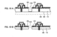
- Figs. 10A and 10B are diagrams for illustrating a method of manufacturing a semiconductor device according to a third embodiment of the present invention.
- the process of removing the bottom portion of the groove 100 is carried out with the material of the semiconductor substrate 10 exposed within the groove 100.
- the groove 100 may be formed, and in order that the insulating layer 28 is not attached, a resist or the like may be provided within the groove 100, or the insulating layer 28 which has entered the groove 100 may be removed.
- Other details are as described in the second embodiment.
- the process of Fig. 3B described in the first embodiment is carried out, and by means of the first etchant, the bottom portion of the groove 100 formed by a part of the semiconductor substrate 10 is etched and removed.
- the bottom portion of the groove 100 is removed from the second surface, and the groove 100 becomes the slit 102. That is to say, the semiconductor substrate 100 is cut along the groove 100.
- Other details are as described in the first and second embodiments.
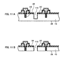
- Figs. 11A and 11B are diagrams for illustrating a method of manufacturing a semiconductor device according to a fourth embodiment of the present invention.
- a groove 110 is formed to be deeper than the depression 22.
- the groove 110 deeper than the depression 22 can be formed easily, exploiting the etching characteristics (the property of etching deeper in a wider spaces).
- the semiconductor substrate 100 is cut along the groove 110.
- the semiconductor substrate 10 is cut while the insulating layer 28 is formed within the groove 110, but the semiconductor substrate 10 may equally be cut while the material of the semiconductor substrate 10 is exposed within the groove 110.
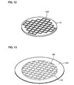
- Fig. 12 is a diagram for illustrating a method of manufacturing a semiconductor device according to a fifth embodiment of the present invention.
- the content of this embodiment can be applied to any from the second to the fourth embodiments.
- a groove 120 is formed only in regions delineating a plurality of semiconductor chips having a plurality of integrated circuits 12 (See Fig. 1A).
- parts of the semiconductor substrate 10 that are not needed do not become separated, and damage to the semiconductor chip forming the product can be prevented.
- Fig. 13 is a diagram for illustrating a method of manufacturing a semiconductor device according to a sixth embodiment of the present invention.
- the step of cutting the semiconductor substrate 10 is carried out after attaching a protective sheet 130 to the first surface 20 of the semiconductor substrate 10.
- the protective sheet 130 may be an adhesive tape or adhesive sheet.
- the present invention is not limited to the above-described embodiments, and various modifications can be made.
- the present invention includes various other configurations substantially the same as the configurations described in the embodiments (in function, method and effect, or in objective and effect, for example).
- the present invention also includes a configuration in which an unsubstantial portion in the described embodiments is replaced.
- the present invention also includes a configuration having the same effects as the configurations described in the embodiments, or a configuration able to achieve the same objective.
- the present invention includes a configuration in which a publicly known technique is added to the configurations in the embodiments.
Landscapes
- Internal Circuitry In Semiconductor Integrated Circuit Devices (AREA)
- Weting (AREA)
- Dicing (AREA)
Abstract
A depression (22) is formed from a first surface (20) of a semiconductor
substrate (10). An insulating layer (28) is provided on the bottom surface and an inner
wall surface of the depression (22). A conductive portion (30) is provided inside the
insulating layer (28). A second surface (38) of the semiconductor substrate (10) is
etched by a first etchant having characteristics such that the etching amount with respect
to the semiconductor substrate (10) is greater than the etching amount with respect to
the insulating layer (28), and the conductive portion (30) is caused to project while
covered by the insulating layer (28). At least a portion of the insulating layer (28)
formed on the bottom surface of the depression (22) is etched with a second etchant
having characteristics such that at least the insulating layer (28) is etched without
forming a residue on the conductive portion (30), to expose the conductive portion (30).
Description
The present invention relates to a semiconductor device and method of
manufacturing the same, a circuit board, and an electronic instrument.
A semiconductor device for three-dimensional mounting has been developed. It
is known to form electrodes penetrating a semiconductor chip, to enable
three-dimensional mounting. The penetrating electrodes are formed to project from the
semiconductor chip. In the conventionally known method of forming a penetrating
electrode, a portion of silicon around the penetrating electrode is etched, whereby the
penetrating electrode is caused to project. In this case, it is difficult to prevent the
projecting portion of the penetrating electrode from being contaminated by the etching
gas.
The present invention solves the existing problems, and has as its object the
formation of a penetrating electrode of high quality.
the first etchant may be one of SF6, CF4, and Cl2 gases.
the step (d) may be carried out using a dry etching device.
the first etchant may be one of a liquid mixture of hydrofluoric acid and nitric acid, and a liquid mixture of hydrofluoric acid, nitric acid, and acetic acid.
the second etchant may be one of a gas mixture of argon and CF4, and a gas mixture of O2 and CF4.
the step (e) may be carried out using a dry etching device.
the second etchant may be one of liquid hydrofluoric acid, and a liquid mixture of hydrofluoric acid and ammonium fluoride.
the insulating layer may be formed of one of SiO2 and SiN.
an outer layer of the conductive portion may also be etched in the step (e).
the outer layer and a central portion of the conductive portion may be formed of different materials.
the central portion of the conductive portion may be formed of one of copper, tungsten, and doped polysilicon.
at least a part of the outer layer of the conductive portion may be formed of one of TiW, TiN, and TaN.
polishing the second surface of the semiconductor substrate up to a point before the insulating layer before the step (d)
the etching of the step (e) may have a lower etching rate with respect to the semiconductor substrate than the etching of the step (d).
the semiconductor substrate may be a semiconductor wafer having a plurality of the integrated circuits, the depression being formed for each of the integrated circuits,
the method further comprising cutting the semiconductor substrate.
the step of cutting the semiconductor substrate may comprise:
the groove may be formed by cutting.
the groove may be formed by etching.
the groove may be formed in the same process as the depression in the step (a).
the groove may be formed to be deeper than the depression; and
a bottom portion of the groove may be removed by the polishing of the second surface of the semiconductor substrate.
the insulating layer may be provided also within the groove in the step (b).
part of the insulating layer formed on a bottom portion of the groove may be caused to project from the second surface in the step (d); and
the part of the insulating layer formed on a bottom portion of the groove may be etched and removed by means of the second etchant in the step (e).
the step of removing the bottom portion of the groove may be carried out in a state that a material of the semiconductor substrate is exposed within the groove.
the bottom portion of the groove formed by a part of the semiconductor substrate may be etched and removed by means of the first etchant in the step (d).
the step of cutting the semiconductor substrate may be carried out with a protective sheet adhered to the first surface of the semiconductor substrate, so that a plurality of semiconductor chips obtained by cutting do not fall apart.
the groove may be formed only in regions sectioning the semiconductor substrate into a plurality of semiconductor chips having the plurality of integrated circuits.
Embodiments of the present invention are now described with reference to the
drawings.
Figs. 1A to 3C are diagrams for illustrating a method of manufacturing a
semiconductor device according to a first embodiment of the present invention. In this
embodiment, a semiconductor substrate 10 is used. The semiconductor substrate 10
shown in Fig. 1A is a semiconductor wafer, but it may be a semiconductor chip. On the
semiconductor substrate 10 is formed at least one (a plurality on a semiconductor wafer;
one on a semiconductor chip) integrated circuit (for example, a circuit comprising
transistors or memory) 12. On the semiconductor substrate 10 are formed a plurality of
electrodes (for example, pads) 14. Each electrode 14 is electrically connected to the
integrated circuit 12. The electrodes 14 may be formed of aluminum. The surface form
of the electrodes 14 is not particularly restricted, but is commonly rectangular. When
the semiconductor substrate 10 is a semiconductor wafer, in each of the regions for the
plurality of semiconductor chips, two or more (one group of) electrodes 14 are formed.
On the semiconductor substrate 10 are formed passivation films 16 and 18, of a
single layer or more layers. The passivation films 16 and 18 can be formed of, for
example, SiO2, SiN, polyimide resin, or the like. In the example shown in Fig. 1A, on
the passivation film 16, the electrodes 14, and interconnecting lines (not shown in the
drawings) connecting the integrated circuit 12 and electrodes 14 are formed. The other
passivation film 18 is formed so as to avoid at least a part of the surface of the
electrodes 14. After forming the passivation film 18 to cover the surface of the
electrodes 14, a part may be etched to expose a part of the electrodes 14. For the etching,
either dry etching or wet etching may be applied. When etching the passivation film 18,
the surface of the electrodes 14 may be etched.
In this embodiment, in the semiconductor substrate 10, a depression 22 (see Fig.
1C) is formed from a first surface 20 thereof. The first surface 20 is the surface on
which the electrodes 14 are formed. The depression 22 is formed to avoid the elements
and interconnecting lines of the integrated circuit 12. As shown in Fig. 1B, a through
hole 24 may be formed in the electrodes 14. To form the through hole 24, etching (dry
etching or wet etching) may be applied. The etching may be carried out after using a
lithography process to form a patterned resist (not shown in the drawings). When the
passivation film 16 is formed beneath the electrodes 14, a through hole 26 (see Fig. 1C)
is also formed therein. When the etching of the electrodes 14 is stopped by the
passivation film 16, for the formation of the through hole 26 the etchant used for
etching the electrodes 14 may be replaced by a different etchant. In this case, once again,
a patterned resist (not shown in the drawings) may be formed by a lithography process.
As shown in Fig. 1C, the depression 22 is formed in the semiconductor
substrate 10 so as to communicate with the through hole 24 (and through hole 26). The
through hole 24 (and through hole 26) and depression 22 can also be referred to
collectively as a depression. For the formation of the depression 22, etching (dry etching
or wet etching) can be applied. Etching may be carried out after forming a patterned
resist (not shown in the drawings) by a lithography process. Alternatively, for the
formation of the depression 22, a laser (for example, a CO2 laser, a YAG laser, or the
like) may be used. The laser may be applied to the formation of the through holes 24
and 26. The depression 22 and through holes 24 and 26 may also be formed together by
the use of a single etchant or laser.
As shown in Fig. 1D, on the inner surface of the depression 22, an insulating
layer 28 is formed. The insulating layer 28 may be an oxidation film. For example, if
the material of the semiconductor substrate 10 is silicon, the insulating layer 28 may be
of SiO2 or SiN. The insulating layer 28 is formed on the bottom surface of the
depression 22. The insulating layer 28 is formed on the inner wall of the depression 22.
However, the insulating layer 28 is formed so as not to fill in the depression 22. That is
to say, a depression is formed by the insulating layer 28. The insulating layer 28 may be
formed on the inner wall of the through hole 26 in the passivation film 16. The
insulating layer 28 may be formed over the passivation film 18.
The insulating layer 28 may be formed on the inner wall of the through hole 24
in the electrodes 14. The insulating layer 28 is formed to avoid a part of the electrodes
14 (for example, the top surface thereof). The insulating layer 28 may be formed to
cover the whole surface of the electrodes 14, and then by partial etching (dry etching or
wet etching), a part of the electrodes 14 exposed. The etching may be carried out after
forming a patterned resist (not shown in the drawings) by a lithography process.
Next, a conductive portion 30 (see Fig. 2B) is provided inside the insulating
layer 28. The conductive portion 30 may be formed of copper, tungsten, or the like. As
shown in Fig. 2A, after an outer layer 32 of the conductive portion 30 is formed, a
central portion 34 thereof may be formed. The central portion 34 can be formed of any
of copper, tungsten, or doped polysilicon (for example, low temperature polysilicon).
The outer layer 32 may include at least a barrier layer. The barrier layer prevents the
material of the central portion 34 or of the seed layer described next from diffusing into
the semiconductor substrate 10 (for example silicon). The barrier layer may be formed
of a different material from the central portion 34 (for example, TiW, TiN, or TaN). If
the central portion 34 is formed by electroplating, the outer layer 32 may include a seed
layer. The seed layer is formed after forming the barrier layer. The seed layer is formed
of the same material (for example copper) as the central portion 34. It should be noted
that the conductive portion 30 (at least the central portion 34 thereof) may be formed by
electroless plating or an inkjet method.
As shown in Fig. 2B, when the outer layer 32 is also formed over the
passivation film 18, as shown in Fig. 2C, the part of the outer layer 32 over the
passivation film 18 is etched. By forming the central portion 34 after the outer layer 32
is formed, the conductive portion 30 can be provided. A part of the conductive portion
30 is positioned within the depression 22 in the semiconductor substrate 10. Between
the inner surface of the depression 22 and the conductive portion 30 is interposed the
insulating layer 28, and therefore the two are electrically isolated. The conductive
portion 30 is electrically connected to the electrodes 14. For example, a portion of the
electrodes 14 exposed from the insulating layer 28 may contact the conductive portion
30. A part of the conductive portion 30 may be positioned over the passivation film 18.
The conductive portion 30 may be provided only within the region of the electrodes 14.
The conductive portion 30 may project, at least above the depression 22. For example,
the conductive portion 30 may project from the passivation film 18.
It should be noted that as a variant, the central portion 34 may be formed with
the outer layer 32 remaining on the passivation film 18. In that case, since a layer
continuous with the central portion 34 is also formed over the passivation film 18, this
layer is etched.
As shown in Fig. 2D, over the conductive portion 30, a brazing material layer
36 may be provided. The brazing material layer 36 is formed, for example, of solder,
and may be formed of either of soft solder or hard solder. The brazing material layer 36
may be formed by covering regions other than the second conductive portion 32 with a
resist. By the above process, bumps can be formed by the conductive portion 30 or with
the addition of the brazing material layer 36.
In this embodiment, as shown in Fig. 3A, a second surface of the
semiconductor substrate 10 (the surface on the opposite side to the first surface 20) may
be removed by, for example, at least one of mechanical polishing or grinding and
chemical polishing or grinding. This process is carried out up to a point before the
insulating layer 28 formed in the depression 22 is exposed. It should be noted that the
process shown in Fig. 3A may be omitted, and next the process of Fig. 3B carried out.
As shown in Fig. 3B, the second surface 38 of the semiconductor substrate 10
is etched so that the insulating layer 28 is exposed. The second surface 38 of the
semiconductor substrate 10 is etched so that the conductive portion 30 (more precisely,
the portion within the depression 22 thereof) projects while covered by the insulating
layer 28. The etching is carried out with a first etchant, whose properties are such as to
yield a greater etching amount with respect to the semiconductor substrate (for example,
a silicon base material) 10 than with respect to the insulating layer (for example, formed
of SiO2) 28. The first etchant may be SF6, CF4, or Cl2 gas. The etching may be carried
out using a dry etching device. Alternatively, the first etchant may be a mixture of
hydrofluoric acid and nitric acid, or a mixture of hydrofluoric acid, nitric acid, and
acetic acid.
As shown in Fig. 3C, at least the portion of the insulating layer 28 formed on
the bottom surface of the depression 22 is etched. Then the conductive portion 30 is
exposed. The extreme surface of the conductive portion 30 may be exposed, and the
peripheral surface of the extremity of the conductive portion 30 covered by the
insulating layer 28. The outer layer 32 (for example, a barrier layer) of the conductive
portion 30 may also be etched. The etching is carried out with a second etchant of
characteristics such as to etch at least the insulating layer 28 without forming residues
on the conductive portion 30. For the second etchant may be used an etchant which does
not react (or has little reaction) with the material (for example, copper) of the
conductive portion 30. The second etchant may be a mixture of argon and CF4 gas, or a
mixture of O2 and CF4 gas. The etching may be carried out using a dry etching device.
Alternatively, the second etchant may be liquid hydrofluoric acid, or a liquid mixture of
hydrofluoric acid and ammonium fluoride. The etching by the second etchant may have
an etching rate with respect to the semiconductor substrate 10 which is slower than
etching by the first etchant.
It should be noted that in at least one step in Figs. 3A to 3C, a reinforcing
member of, for example, resin layer or resin tape may be provided on the first surface
20 of the semiconductor substrate 10.
By the above process, the conductive portion 30 can be caused to project from
the second surface 38 of the semiconductor substrate 10. The projecting conductive
portion 30 forms a projecting electrode. The conductive portion 30 also forms
penetrating electrodes of the first and second surfaces 20 and 38. According to this
embodiment, when exposing the conductive portion 30 from the insulating layer 28,
since no residues are left on the conductive portion 30, penetrating electrodes of high
quality can be formed.
As shown in Fig. 4, when the semiconductor substrate 10 is a semiconductor
wafer, concavities 22 may be formed corresponding to individual integrated circuits 12
(See Fig. 1A), and the semiconductor substrate 10 may be cut (for example, by dicing).
For the cutting, a cutter (for example, a dicer) 40 or laser (for example, a CO2 laser,
YAG laser, or the like) may be used.
By the above process, a semiconductor device can be manufactured. As shown
in Fig. 5, a plurality of semiconductor devices manufactured by the above described
method may be laminated, and electrical connection therebetween may be achieved
through respective conductive portions 30. This embodiment is effective for carrying
out such a three-dimensional mounting. The semiconductor device shown in Fig. 5 has a
plurality of semiconductor substrates 10. In the direction of the first surface 20, the
outermost positioned (in Fig. 5, the lowest) semiconductor substrate 10 has external
terminals (for example, solder balls) 42. The external terminals 42 are provided, on
interconnecting lines 46 formed over a resin layer (for example, a stress relieving layer)
44. The interconnecting lines 46 are connected to the conductive portion 30 on the first
surface 20.
In Fig. 6 is shown a circuit board 1000 on which is mounted a semiconductor
device 1, formed of a laminated plurality of semiconductor chips. The plurality of
semiconductor chips is electrically connected by the above described conductive portion
30. As an electronic instrument having the above described semiconductor device, Fig.
7 shows a notebook personal computer 2000, and Fig. 8 shows a mobile telephone
3000.
Figs. 9A to 9C are diagrams for illustrating a method of manufacturing a
semiconductor device according to a second embodiment of the present invention. In
this embodiment, a groove 100 is formed in the semiconductor substrate 10 (more
precisely, in the first surface 20 thereof). The groove 100 is formed along the cutting
line of the semiconductor substrate 10. The groove 100 may be formed by cutting, or
may be formed by etching. The groove 100 may be formed in the step of forming the
depression 22 shown in Fig. 1C, with the same process (for example, at the same time)
as the depression 22. The insulating layer 28 may be provided within the groove 100.
The groove 100 may be of substantially the same depth as the depression 22, or may be
deeper than the depression 22, or may be shallower than the depression 22.
Thereafter, the process described in Figs. 3A to 3C in the first embodiment is
carried out. Figs. 9A to 9C show the configuration in the vicinity of the groove 100
when the respective steps shown in Figs. 3A to 3C are carried out. For example, the
process shown in Fig. 3A is carried out, and the second surface 38 of the semiconductor
substrate 10 is polished to a point short of the insulating layer 28 (see Fig. 9A). The
process shown in Fig. 3B is carried out, as shown in Fig. 9B, and the insulating layer 28
formed at the bottom of the groove 100 is caused to project from the second surface 38.
Then, the process shown in Fig. 3C is carried out, as shown in Fig. 9C, and by
means of the second etchant, the insulating layer 28 formed at the bottom of the groove
100 is etched and removed. In this way, the bottom portion of the groove 100 is
removed from the second surface, and the groove 100 becomes a slit 102. That is to say,
the semiconductor substrate 100 is cut along the groove 100.
According to this embodiment, the semiconductor substrate 10 can be cut
simply. Since final cutting of the semiconductor substrate 10 is carried out by means of
the second etchant, chipping is not likely to occur. Furthermore, in this embodiment,
since the insulating layer 28 is formed within the groove 100, the semiconductor chip
has the insulating layer 28 on the edge surface. Therefore, this semiconductor chip is
not susceptible to edge shorting. Other details are as described in the first embodiment.
Figs. 10A and 10B are diagrams for illustrating a method of manufacturing a
semiconductor device according to a third embodiment of the present invention. In this
embodiment, as shown in Fig. 10A, the process of removing the bottom portion of the
groove 100 is carried out with the material of the semiconductor substrate 10 exposed
within the groove 100. For example, after carrying out the process of forming the
insulating layer 28 shown in Fig. 1D within the depression 22, the groove 100 may be
formed, and in order that the insulating layer 28 is not attached, a resist or the like may
be provided within the groove 100, or the insulating layer 28 which has entered the
groove 100 may be removed. Other details are as described in the second embodiment.
In this embodiment, the process of Fig. 3B described in the first embodiment is
carried out, and by means of the first etchant, the bottom portion of the groove 100
formed by a part of the semiconductor substrate 10 is etched and removed. In this way,
as shown in Fig. 10B, the bottom portion of the groove 100 is removed from the second
surface, and the groove 100 becomes the slit 102. That is to say, the semiconductor
substrate 100 is cut along the groove 100. Other details are as described in the first and
second embodiments.
Figs. 11A and 11B are diagrams for illustrating a method of manufacturing a
semiconductor device according to a fourth embodiment of the present invention. In this
embodiment, as shown in Fig. 11A, a groove 110 is formed to be deeper than the
depression 22. The groove 110 deeper than the depression 22 can be formed easily,
exploiting the etching characteristics (the property of etching deeper in a wider spaces).
Then as shown in Fig. Fig. 11B, by polishing the second surface 38 of the
semiconductor substrate 10 (refer to the description relating to Fig. 3A), the bottom
portion of the groove 110 is removed. In this way, the bottom portion of the groove 110
is removed from the second surface, and the groove 110 becomes a slit 112. That is to
say, the semiconductor substrate 100 is cut along the groove 110. Other details are as
described in the first, second, and third embodiments. In this embodiment, the
semiconductor substrate 10 is cut while the insulating layer 28 is formed within the
groove 110, but the semiconductor substrate 10 may equally be cut while the material of
the semiconductor substrate 10 is exposed within the groove 110.
Fig. 12 is a diagram for illustrating a method of manufacturing a
semiconductor device according to a fifth embodiment of the present invention. The
content of this embodiment can be applied to any from the second to the fourth
embodiments. In this embodiment, a groove 120 is formed only in regions delineating a
plurality of semiconductor chips having a plurality of integrated circuits 12 (See Fig.
1A). By this means, parts of the semiconductor substrate 10 that are not needed (for
example, an outer peripheral portion) do not become separated, and damage to the
semiconductor chip forming the product can be prevented.
Fig. 13 is a diagram for illustrating a method of manufacturing a
semiconductor device according to a sixth embodiment of the present invention. In this
embodiment, the step of cutting the semiconductor substrate 10 is carried out after
attaching a protective sheet 130 to the first surface 20 of the semiconductor substrate 10.
The protective sheet 130 may be an adhesive tape or adhesive sheet. By means of this,
even when the semiconductor substrate 10 is cut, the plurality of semiconductor chips
does not fall apart. The content of this embodiment can be applied to any from the first
to the fifth embodiments.
The present invention is not limited to the above-described embodiments, and
various modifications can be made. For example, the present invention includes various
other configurations substantially the same as the configurations described in the
embodiments (in function, method and effect, or in objective and effect, for example).
The present invention also includes a configuration in which an unsubstantial portion in
the described embodiments is replaced. The present invention also includes a
configuration having the same effects as the configurations described in the
embodiments, or a configuration able to achieve the same objective. Further, the
present invention includes a configuration in which a publicly known technique is
added to the configurations in the embodiments.
Claims (33)
- A method of manufacturing a semiconductor device comprising:(a) forming a depression from a first surface of a semiconductor substrate in which an integrated circuit is formed;(b) providing an insulating layer on the bottom surface and an inner wall surface of the depression;(c) providing a conductive portion inside the insulating layer;(d) etching a second surface of the semiconductor substrate opposite to the first surface, with a first etchant having characteristics such that the etching amount with respect to the semiconductor substrate is greater than the etching amount with respect to the insulating layer, to cause the conductive portion to project while covered by the insulating layer;(e) etching at least a portion of the insulating layer formed on the bottom surface of the depression with a second etchant having characteristics such that at least the insulating layer is etched without forming a residue on the conductive portion, to expose the conductive portion.
- The method as defined in claim 1,
wherein the first etchant is one of SF6, CF4, and Cl2 gases. - The method as defined in claim 2,
wherein the step (d) is carried out using a dry etching device. - The method as defined in claim 1,
wherein the first etchant is one of a liquid mixture of hydrofluoric acid and nitric acid, and a liquid mixture of hydrofluoric acid, nitric acid, and acetic acid. - The method as defined in claim 1,
wherein the second etchant is one of a gas mixture of argon and CF4, and a gas mixture of O2 and CF4. - The method as defined in claim 5,
wherein the step (e) is carried out using a dry etching device. - The method as defined in claim 1,
wherein the second etchant is one of liquid hydrofluoric acid, and a liquid mixture of hydrofluoric acid and ammonium fluoride. - The method as defined in claim 1,
wherein the insulating layer is formed of one of SiO2 and SiN. - The method as defined in claim 1,
wherein an outer layer of the conductive portion is also etched in the step (e). - The method as defined in claim 9,
wherein the outer layer and a central portion of the conductive portion are formed of different materials. - The method as defined in claim 10,
wherein the central portion of the conductive portion is formed of one of copper, tungsten, and doped polysilicon. - The method as defined in claim 10,
wherein at least a part of the outer layer of the conductive portion is formed of one of TiW, TiN, and TaN. - The method as defined in claim 1, further comprising:polishing the second surface of the semiconductor substrate up to a point before the insulating layer before the step (d).
- The method as defined in claim 1,
wherein the etching of the step (e) has a lower etching rate with respect to the semiconductor substrate than the etching of the step (d). - The method as defined in claim 1,
wherein the semiconductor substrate is a semiconductor wafer having a plurality of the integrated circuits, the depression being formed for each of the integrated circuits,
the method further comprising cutting the semiconductor substrate. - The method as defined in claim 15,
wherein the step of cutting the semiconductor substrate comprises:forming a groove in the first surface, along a cutting line of the semiconductor substrate; andremoving a bottom portion of the groove from the second surface so that the groove becomes a slit. - The method as defined in claim 16,
wherein the groove is formed by cutting. - The method as defined in claim 16,
wherein the groove is formed by etching. - The method as defined in claim 16,
wherein the groove is formed in the same process as the depression in the step (a). - The method as defined in claim 16, further comprising:wherein the groove is formed to be deeper than the depression; andpolishing the second surface of the semiconductor substrate up to a point before the insulating layer before the step (d),
wherein a bottom portion of the groove is removed by the polishing of the second surface of the semiconductor substrate. - The method as defined in claim 16,
wherein the insulating layer is provided also within the groove in the step (b). - The method as defined in claim 21,
wherein part of the insulating layer formed on a bottom portion of the groove is caused to project from the second surface in the step (d); and
wherein the part of the insulating layer formed on a bottom portion of the groove is etched and removed by means of the second etchant in the step (e). - The method as defined in claim 16,
wherein the step of removing the bottom portion of the groove is carried out in a state that a material of the semiconductor substrate is exposed within the groove. - The method as defined in claim 23,
wherein the bottom portion of the groove formed by a part of the semiconductor substrate is etched and removed by means of the first etchant in the step (d). - The method as defined in claim 16,
wherein the step of cutting the semiconductor substrate is carried out with a protective sheet adhered to the first surface of the semiconductor substrate, so that a plurality of semiconductor chips obtained by cutting do not fall apart. - The method as defined in claim 16,
wherein the groove is formed only in regions sectioning the semiconductor substrate into a plurality of semiconductor chips having the plurality of integrated circuits. - A method of manufacturing a semiconductor device, comprising:laminating a plurality of semiconductor devices manufactured by the method as defined in any one of claims 1 to 26; andmaking electrical connections between the semiconductor devices through the conductive portions.
- A semiconductor device manufactured by the method as defined in any one of claims 1 to 26.
- A semiconductor device manufactured by the method as defined in claim 27.
- A circuit board on which is mounted the semiconductor device as defined in claim 28.
- A circuit board on which is mounted the semiconductor device as defined in claim 29.
- An electronic instrument having the semiconductor device as defined in claim 28.
- An electronic instrument having the semiconductor device as defined in claim 29.
Applications Claiming Priority (5)
| Application Number | Priority Date | Filing Date | Title |
|---|---|---|---|
| JP2002076308 | 2002-03-19 | ||
| JP2002076308 | 2002-03-19 | ||
| JP2003007277A JP4110390B2 (en) | 2002-03-19 | 2003-01-15 | Manufacturing method of semiconductor device |
| JP2003007277 | 2003-01-15 | ||
| PCT/JP2003/003302 WO2003079431A1 (en) | 2002-03-19 | 2003-03-19 | Semiconductor device and its manufacturing method, circuit board, and electric apparatus |
Publications (2)
| Publication Number | Publication Date |
|---|---|
| EP1391924A1 true EP1391924A1 (en) | 2004-02-25 |
| EP1391924A4 EP1391924A4 (en) | 2005-06-15 |
Family
ID=28043775
Family Applications (1)
| Application Number | Title | Priority Date | Filing Date |
|---|---|---|---|
| EP03710425A Withdrawn EP1391924A4 (en) | 2002-03-19 | 2003-03-19 | SEMICONDUCTOR DEVICE, METHOD OF MANUFACTURE, CIRCUIT BOARD, AND ELECTRICAL APPARATUS |
Country Status (7)
| Country | Link |
|---|---|
| US (1) | US7029937B2 (en) |
| EP (1) | EP1391924A4 (en) |
| JP (1) | JP4110390B2 (en) |
| KR (1) | KR100552987B1 (en) |
| CN (1) | CN1279604C (en) |
| TW (1) | TWI282592B (en) |
| WO (1) | WO2003079431A1 (en) |
Cited By (4)
| Publication number | Priority date | Publication date | Assignee | Title |
|---|---|---|---|---|
| EP1553625A1 (en) * | 2004-01-12 | 2005-07-13 | Infineon Technologies AG | Method for fabrication of a contact structure |
| WO2007092176A2 (en) | 2006-02-03 | 2007-08-16 | Micron Technology, Inc. | Methods for fabricating and filling conductive vias and conductive vias so formed |
| WO2009000258A1 (en) * | 2007-06-22 | 2008-12-31 | Fraunhofer-Gesellschaft zur Förderung der angewandten Forschung e.V. | Method for producing substrates |
| DE102004044946B4 (en) * | 2003-09-25 | 2012-02-09 | Disco Corp. | Method for separating a semiconductor wafer |
Families Citing this family (40)
| Publication number | Priority date | Publication date | Assignee | Title |
|---|---|---|---|---|
| US6809421B1 (en) | 1996-12-02 | 2004-10-26 | Kabushiki Kaisha Toshiba | Multichip semiconductor device, chip therefor and method of formation thereof |
| US7233413B2 (en) | 2002-11-22 | 2007-06-19 | E. I. Du Pont De Nemours And Company | Gamut description and visualization |
| JP4035034B2 (en) * | 2002-11-29 | 2008-01-16 | 株式会社ルネサステクノロジ | Semiconductor device and manufacturing method thereof |
| JP4072677B2 (en) * | 2003-01-15 | 2008-04-09 | セイコーエプソン株式会社 | Semiconductor chip, semiconductor wafer, semiconductor device and manufacturing method thereof, circuit board, and electronic equipment |
| TWI239629B (en) | 2003-03-17 | 2005-09-11 | Seiko Epson Corp | Method of manufacturing semiconductor device, semiconductor device, circuit substrate and electronic apparatus |
| US8084866B2 (en) | 2003-12-10 | 2011-12-27 | Micron Technology, Inc. | Microelectronic devices and methods for filling vias in microelectronic devices |
| US7091124B2 (en) | 2003-11-13 | 2006-08-15 | Micron Technology, Inc. | Methods for forming vias in microelectronic devices, and methods for packaging microelectronic devices |
| JP3698160B2 (en) | 2004-01-09 | 2005-09-21 | セイコーエプソン株式会社 | Manufacturing method of semiconductor device |
| JP4850392B2 (en) * | 2004-02-17 | 2012-01-11 | 三洋電機株式会社 | Manufacturing method of semiconductor device |
| JP3945493B2 (en) * | 2004-04-16 | 2007-07-18 | セイコーエプソン株式会社 | Semiconductor device and manufacturing method thereof |
| US20050247894A1 (en) | 2004-05-05 | 2005-11-10 | Watkins Charles M | Systems and methods for forming apertures in microfeature workpieces |
| KR100618543B1 (en) * | 2004-06-15 | 2006-08-31 | 삼성전자주식회사 | Chip Scale Package Manufacturing Method for Wafer-Level Stacking Packages |
| US7232754B2 (en) * | 2004-06-29 | 2007-06-19 | Micron Technology, Inc. | Microelectronic devices and methods for forming interconnects in microelectronic devices |
| US7425499B2 (en) | 2004-08-24 | 2008-09-16 | Micron Technology, Inc. | Methods for forming interconnects in vias and microelectronic workpieces including such interconnects |
| SG120200A1 (en) * | 2004-08-27 | 2006-03-28 | Micron Technology Inc | Slanted vias for electrical circuits on circuit boards and other substrates |
| US7109068B2 (en) * | 2004-08-31 | 2006-09-19 | Micron Technology, Inc. | Through-substrate interconnect fabrication methods |
| US7300857B2 (en) * | 2004-09-02 | 2007-11-27 | Micron Technology, Inc. | Through-wafer interconnects for photoimager and memory wafers |
| TWI288448B (en) * | 2004-09-10 | 2007-10-11 | Toshiba Corp | Semiconductor device and method of manufacturing the same |
| US7271482B2 (en) | 2004-12-30 | 2007-09-18 | Micron Technology, Inc. | Methods for forming interconnects in microelectronic workpieces and microelectronic workpieces formed using such methods |
| US20060177999A1 (en) * | 2005-02-10 | 2006-08-10 | Micron Technology, Inc. | Microelectronic workpieces and methods for forming interconnects in microelectronic workpieces |
| US7795134B2 (en) | 2005-06-28 | 2010-09-14 | Micron Technology, Inc. | Conductive interconnect structures and formation methods using supercritical fluids |
| US7429529B2 (en) * | 2005-08-05 | 2008-09-30 | Farnworth Warren M | Methods of forming through-wafer interconnects and structures resulting therefrom |
| US7622377B2 (en) | 2005-09-01 | 2009-11-24 | Micron Technology, Inc. | Microfeature workpiece substrates having through-substrate vias, and associated methods of formation |
| US7517798B2 (en) * | 2005-09-01 | 2009-04-14 | Micron Technology, Inc. | Methods for forming through-wafer interconnects and structures resulting therefrom |
| US7863187B2 (en) | 2005-09-01 | 2011-01-04 | Micron Technology, Inc. | Microfeature workpieces and methods for forming interconnects in microfeature workpieces |
| US7262134B2 (en) | 2005-09-01 | 2007-08-28 | Micron Technology, Inc. | Microfeature workpieces and methods for forming interconnects in microfeature workpieces |
| US7749899B2 (en) | 2006-06-01 | 2010-07-06 | Micron Technology, Inc. | Microelectronic workpieces and methods and systems for forming interconnects in microelectronic workpieces |
| US7629249B2 (en) | 2006-08-28 | 2009-12-08 | Micron Technology, Inc. | Microfeature workpieces having conductive interconnect structures formed by chemically reactive processes, and associated systems and methods |
| US7902643B2 (en) | 2006-08-31 | 2011-03-08 | Micron Technology, Inc. | Microfeature workpieces having interconnects and conductive backplanes, and associated systems and methods |
| JP2008071831A (en) * | 2006-09-12 | 2008-03-27 | Teoss Corp | IC chip provided with through electrode, and method of manufacturing the IC chip |
| JP5103854B2 (en) * | 2006-10-02 | 2012-12-19 | セイコーエプソン株式会社 | SEMICONDUCTOR DEVICE, SEMICONDUCTOR DEVICE MANUFACTURING METHOD, CIRCUIT BOARD AND ELECTRONIC DEVICE |
| KR100844997B1 (en) * | 2006-12-29 | 2008-07-09 | 삼성전자주식회사 | Semiconductor package, semiconductor stack package, method of manufacturing the packages |
| SG150410A1 (en) | 2007-08-31 | 2009-03-30 | Micron Technology Inc | Partitioned through-layer via and associated systems and methods |
| US7884015B2 (en) | 2007-12-06 | 2011-02-08 | Micron Technology, Inc. | Methods for forming interconnects in microelectronic workpieces and microelectronic workpieces formed using such methods |
| US20100207227A1 (en) * | 2009-02-16 | 2010-08-19 | Georg Meyer-Berg | Electronic Device and Method of Manufacturing Same |
| US8541305B2 (en) | 2010-05-24 | 2013-09-24 | Institute of Microelectronics, Chinese Academy of Sciences | 3D integrated circuit and method of manufacturing the same |
| CN102263099B (en) * | 2010-05-24 | 2013-09-18 | 中国科学院微电子研究所 | 3D integrated circuit and its manufacturing method |
| US8952542B2 (en) * | 2012-11-14 | 2015-02-10 | Advanced Semiconductor Engineering, Inc. | Method for dicing a semiconductor wafer having through silicon vias and resultant structures |
| CN104143526B (en) * | 2013-05-09 | 2019-05-17 | 盛美半导体设备(上海)有限公司 | Through Silicon Via Structure Fabrication Method |
| WO2016020516A1 (en) * | 2014-08-08 | 2016-02-11 | Basf Se | Electroluminescent imidazo-quinoxaline carbene metal complexes |
Family Cites Families (26)
| Publication number | Priority date | Publication date | Assignee | Title |
|---|---|---|---|---|
| JPS607148A (en) * | 1983-06-24 | 1985-01-14 | Nec Corp | Manufacture of semiconductor device |
| JPS607149A (en) * | 1983-06-24 | 1985-01-14 | Nec Corp | Manufacture of semiconductor device |
| JPS6098655A (en) * | 1983-11-02 | 1985-06-01 | Nec Corp | Semiconductor device |
| JPS6098654A (en) * | 1983-11-02 | 1985-06-01 | Nec Corp | Manufacture of semiconductor device |
| JPS60235446A (en) * | 1984-05-09 | 1985-11-22 | Nec Corp | Semiconductor device and manufacture thereof |
| JP2562477B2 (en) * | 1988-03-25 | 1996-12-11 | 富士通株式会社 | Method for manufacturing semiconductor device |
| US4978639A (en) * | 1989-01-10 | 1990-12-18 | Avantek, Inc. | Method for the simultaneous formation of via-holes and wraparound plating on semiconductor chips |
| JPH0831617B2 (en) * | 1990-04-18 | 1996-03-27 | 三菱電機株式会社 | Solar cell and manufacturing method thereof |
| DE69233314T2 (en) * | 1991-10-11 | 2005-03-24 | Canon K.K. | Process for the production of semiconductor products |
| DE4314907C1 (en) * | 1993-05-05 | 1994-08-25 | Siemens Ag | Method for producing semiconductor components making electrically conducting contact with one another vertically |
| BE1008384A3 (en) * | 1994-05-24 | 1996-04-02 | Koninkl Philips Electronics Nv | METHOD FOR MANUFACTURING SEMICONDUCTOR DEVICES WITH SEMICONDUCTOR ELEMENTS MADE IN A LAYER SEMICONDUCTOR MATERIAL APPLIED ON A BEARING PLATE. |
| US6882030B2 (en) * | 1996-10-29 | 2005-04-19 | Tru-Si Technologies, Inc. | Integrated circuit structures with a conductor formed in a through hole in a semiconductor substrate and protruding from a surface of the substrate |
| US6448153B2 (en) * | 1996-10-29 | 2002-09-10 | Tru-Si Technologies, Inc. | Thinning and dicing of semiconductor wafers using dry etch, and obtaining semiconductor chips with rounded bottom edges and corners |
| US6498074B2 (en) * | 1996-10-29 | 2002-12-24 | Tru-Si Technologies, Inc. | Thinning and dicing of semiconductor wafers using dry etch, and obtaining semiconductor chips with rounded bottom edges and corners |
| JP3537447B2 (en) * | 1996-10-29 | 2004-06-14 | トル‐シ・テクノロジーズ・インコーポレイテッド | Integrated circuit and manufacturing method thereof |
| JP3792954B2 (en) * | 1999-08-10 | 2006-07-05 | 株式会社東芝 | Manufacturing method of semiconductor device |
| US6322903B1 (en) * | 1999-12-06 | 2001-11-27 | Tru-Si Technologies, Inc. | Package of integrated circuits and vertical integration |
| EP1126477A3 (en) * | 2000-02-14 | 2003-06-18 | Leica Microsystems Lithography GmbH | Method for structure investigation in a semiconductor substrate |
| JP3778256B2 (en) * | 2000-02-28 | 2006-05-24 | セイコーエプソン株式会社 | Semiconductor device and manufacturing method thereof, circuit board, and electronic apparatus |
| JP2001326325A (en) * | 2000-05-16 | 2001-11-22 | Seiko Epson Corp | Semiconductor device and manufacturing method thereof |
| US6717254B2 (en) * | 2001-02-22 | 2004-04-06 | Tru-Si Technologies, Inc. | Devices having substrates with opening passing through the substrates and conductors in the openings, and methods of manufacture |
| US6498381B2 (en) * | 2001-02-22 | 2002-12-24 | Tru-Si Technologies, Inc. | Semiconductor structures having multiple conductive layers in an opening, and methods for fabricating same |
| JP4408006B2 (en) * | 2001-06-28 | 2010-02-03 | 富士通マイクロエレクトロニクス株式会社 | Semiconductor device and manufacturing method thereof |
| US6787916B2 (en) * | 2001-09-13 | 2004-09-07 | Tru-Si Technologies, Inc. | Structures having a substrate with a cavity and having an integrated circuit bonded to a contact pad located in the cavity |
| CN1279605C (en) | 2002-03-19 | 2006-10-11 | 精工爱普生株式会社 | Semiconductor device and its producing method, circuit board and electronic instrment |
| US6730540B2 (en) * | 2002-04-18 | 2004-05-04 | Tru-Si Technologies, Inc. | Clock distribution networks and conductive lines in semiconductor integrated circuits |
-
2003
- 2003-01-15 JP JP2003007277A patent/JP4110390B2/en not_active Expired - Lifetime
- 2003-03-19 CN CNB038007061A patent/CN1279604C/en not_active Expired - Lifetime
- 2003-03-19 WO PCT/JP2003/003302 patent/WO2003079431A1/en not_active Ceased
- 2003-03-19 EP EP03710425A patent/EP1391924A4/en not_active Withdrawn
- 2003-03-19 TW TW092106054A patent/TWI282592B/en not_active IP Right Cessation
- 2003-03-19 KR KR1020037015902A patent/KR100552987B1/en not_active Expired - Fee Related
- 2003-11-10 US US10/703,573 patent/US7029937B2/en not_active Expired - Lifetime
Cited By (9)
| Publication number | Priority date | Publication date | Assignee | Title |
|---|---|---|---|---|
| DE102004044946B4 (en) * | 2003-09-25 | 2012-02-09 | Disco Corp. | Method for separating a semiconductor wafer |
| EP1553625A1 (en) * | 2004-01-12 | 2005-07-13 | Infineon Technologies AG | Method for fabrication of a contact structure |
| US7176128B2 (en) | 2004-01-12 | 2007-02-13 | Infineon Technologies Ag | Method for fabrication of a contact structure |
| WO2007092176A2 (en) | 2006-02-03 | 2007-08-16 | Micron Technology, Inc. | Methods for fabricating and filling conductive vias and conductive vias so formed |
| WO2007092176A3 (en) * | 2006-02-03 | 2007-11-08 | Micron Technology Inc | Methods for fabricating and filling conductive vias and conductive vias so formed |
| US7892972B2 (en) | 2006-02-03 | 2011-02-22 | Micron Technology, Inc. | Methods for fabricating and filling conductive vias and conductive vias so formed |
| US8294273B2 (en) | 2006-02-03 | 2012-10-23 | Micron Technology, Inc. | Methods for fabricating and filling conductive vias and conductive vias so formed |
| US8324100B2 (en) | 2006-02-03 | 2012-12-04 | Micron Technology, Inc. | Methods of forming conductive vias |
| WO2009000258A1 (en) * | 2007-06-22 | 2008-12-31 | Fraunhofer-Gesellschaft zur Förderung der angewandten Forschung e.V. | Method for producing substrates |
Also Published As
| Publication number | Publication date |
|---|---|
| CN1533603A (en) | 2004-09-29 |
| EP1391924A4 (en) | 2005-06-15 |
| KR100552987B1 (en) | 2006-02-15 |
| JP4110390B2 (en) | 2008-07-02 |
| TWI282592B (en) | 2007-06-11 |
| TW200305229A (en) | 2003-10-16 |
| US20040142574A1 (en) | 2004-07-22 |
| KR20040012898A (en) | 2004-02-11 |
| WO2003079431A1 (en) | 2003-09-25 |
| JP2003347474A (en) | 2003-12-05 |
| CN1279604C (en) | 2006-10-11 |
| US7029937B2 (en) | 2006-04-18 |
Similar Documents
| Publication | Publication Date | Title |
|---|---|---|
| US7029937B2 (en) | Semiconductor device and method of manufacturing the same, circuit board, and electronic instrument | |
| US6841849B2 (en) | Semiconductor device and method of manufacturing the same, circuit board and electronic instrument | |
| JP3918935B2 (en) | Manufacturing method of semiconductor device | |
| CN100438022C (en) | Semiconductor device, manufacturing method thereof, circuit substrate, and electronic device | |
| CN100367452C (en) | Semiconductor device and manufacturing method thereof | |
| US7795140B2 (en) | Method of manufacturing substrate | |
| US7138710B2 (en) | Semiconductor device and method of manufacturing the same, circuit board, and electronic instrument | |
| JP3972846B2 (en) | Manufacturing method of semiconductor device | |
| JP4349278B2 (en) | Manufacturing method of semiconductor device | |
| US20040192033A1 (en) | Semiconductor device, method of manufacturing the same, circuit board, and electronic instrument | |
| JP3690407B2 (en) | Manufacturing method of semiconductor device | |
| KR20030084701A (en) | A semiconductor device and a method of manufacturing the same, a circuit board and an electronic apparatus | |
| US7193297B2 (en) | Semiconductor device, method for manufacturing the same, circuit substrate and electronic device | |
| JP3698160B2 (en) | Manufacturing method of semiconductor device | |
| JP2004221350A (en) | Semiconductor chip, semiconductor wafer, semiconductor device and manufacturing method thereof, circuit board, and electronic equipment | |
| JP2004221351A (en) | Semiconductor device and its manufacturing method, circuit board, and electronic equipment | |
| JP2005033105A (en) | Semiconductor device and manufacturing method thereof, circuit board, and electronic apparatus |
Legal Events
| Date | Code | Title | Description |
|---|---|---|---|
| PUAI | Public reference made under article 153(3) epc to a published international application that has entered the european phase |
Free format text: ORIGINAL CODE: 0009012 |
|
| 17P | Request for examination filed |
Effective date: 20031127 |
|
| AK | Designated contracting states |
Kind code of ref document: A1 Designated state(s): AT BE BG CH CY CZ DE DK EE ES FI FR GB GR HU IE IT LI LU MC NL PT RO SE SI SK TR |
|
| A4 | Supplementary search report drawn up and despatched |
Effective date: 20050502 |
|
| 17Q | First examination report despatched |
Effective date: 20071128 |
|
| STAA | Information on the status of an ep patent application or granted ep patent |
Free format text: STATUS: THE APPLICATION IS DEEMED TO BE WITHDRAWN |
|
| 18D | Application deemed to be withdrawn |
Effective date: 20080409 |