EP1391923A1 - Semiconductor device and its manufacturing method, circuit board and electronic apparatus - Google Patents
Semiconductor device and its manufacturing method, circuit board and electronic apparatus Download PDFInfo
- Publication number
- EP1391923A1 EP1391923A1 EP03710424A EP03710424A EP1391923A1 EP 1391923 A1 EP1391923 A1 EP 1391923A1 EP 03710424 A EP03710424 A EP 03710424A EP 03710424 A EP03710424 A EP 03710424A EP 1391923 A1 EP1391923 A1 EP 1391923A1
- Authority
- EP
- European Patent Office
- Prior art keywords
- semiconductor device
- conductive portion
- semiconductor substrate
- manufacturing
- insulating layer
- Prior art date
- Legal status (The legal status is an assumption and is not a legal conclusion. Google has not performed a legal analysis and makes no representation as to the accuracy of the status listed.)
- Granted
Links
Images





Classifications
-
- H—ELECTRICITY
- H10—SEMICONDUCTOR DEVICES; ELECTRIC SOLID-STATE DEVICES NOT OTHERWISE PROVIDED FOR
- H10W—GENERIC PACKAGES, INTERCONNECTIONS, CONNECTORS OR OTHER CONSTRUCTIONAL DETAILS OF DEVICES COVERED BY CLASS H10
- H10W72/00—Interconnections or connectors in packages
- H10W72/90—Bond pads, in general
-
- H—ELECTRICITY
- H10—SEMICONDUCTOR DEVICES; ELECTRIC SOLID-STATE DEVICES NOT OTHERWISE PROVIDED FOR
- H10W—GENERIC PACKAGES, INTERCONNECTIONS, CONNECTORS OR OTHER CONSTRUCTIONAL DETAILS OF DEVICES COVERED BY CLASS H10
- H10W20/00—Interconnections in chips, wafers or substrates
- H10W20/01—Manufacture or treatment
-
- H—ELECTRICITY
- H10—SEMICONDUCTOR DEVICES; ELECTRIC SOLID-STATE DEVICES NOT OTHERWISE PROVIDED FOR
- H10P—GENERIC PROCESSES OR APPARATUS FOR THE MANUFACTURE OR TREATMENT OF DEVICES COVERED BY CLASS H10
- H10P54/00—Cutting or separating of wafers, substrates or parts of devices
-
- H—ELECTRICITY
- H10—SEMICONDUCTOR DEVICES; ELECTRIC SOLID-STATE DEVICES NOT OTHERWISE PROVIDED FOR
- H10W—GENERIC PACKAGES, INTERCONNECTIONS, CONNECTORS OR OTHER CONSTRUCTIONAL DETAILS OF DEVICES COVERED BY CLASS H10
- H10W20/00—Interconnections in chips, wafers or substrates
- H10W20/01—Manufacture or treatment
- H10W20/021—Manufacture or treatment of interconnections within wafers or substrates
- H10W20/023—Manufacture or treatment of interconnections within wafers or substrates the interconnections being through-semiconductor vias
-
- H—ELECTRICITY
- H10—SEMICONDUCTOR DEVICES; ELECTRIC SOLID-STATE DEVICES NOT OTHERWISE PROVIDED FOR
- H10W—GENERIC PACKAGES, INTERCONNECTIONS, CONNECTORS OR OTHER CONSTRUCTIONAL DETAILS OF DEVICES COVERED BY CLASS H10
- H10W20/00—Interconnections in chips, wafers or substrates
- H10W20/01—Manufacture or treatment
- H10W20/021—Manufacture or treatment of interconnections within wafers or substrates
- H10W20/023—Manufacture or treatment of interconnections within wafers or substrates the interconnections being through-semiconductor vias
- H10W20/0238—Manufacture or treatment of interconnections within wafers or substrates the interconnections being through-semiconductor vias comprising etching via holes through pads or through electrodes
-
- H—ELECTRICITY
- H10—SEMICONDUCTOR DEVICES; ELECTRIC SOLID-STATE DEVICES NOT OTHERWISE PROVIDED FOR
- H10W—GENERIC PACKAGES, INTERCONNECTIONS, CONNECTORS OR OTHER CONSTRUCTIONAL DETAILS OF DEVICES COVERED BY CLASS H10
- H10W20/00—Interconnections in chips, wafers or substrates
- H10W20/01—Manufacture or treatment
- H10W20/021—Manufacture or treatment of interconnections within wafers or substrates
- H10W20/023—Manufacture or treatment of interconnections within wafers or substrates the interconnections being through-semiconductor vias
- H10W20/0245—Manufacture or treatment of interconnections within wafers or substrates the interconnections being through-semiconductor vias comprising use of blind vias during the manufacture
-
- H—ELECTRICITY
- H10—SEMICONDUCTOR DEVICES; ELECTRIC SOLID-STATE DEVICES NOT OTHERWISE PROVIDED FOR
- H10W—GENERIC PACKAGES, INTERCONNECTIONS, CONNECTORS OR OTHER CONSTRUCTIONAL DETAILS OF DEVICES COVERED BY CLASS H10
- H10W20/00—Interconnections in chips, wafers or substrates
- H10W20/01—Manufacture or treatment
- H10W20/021—Manufacture or treatment of interconnections within wafers or substrates
- H10W20/023—Manufacture or treatment of interconnections within wafers or substrates the interconnections being through-semiconductor vias
- H10W20/0249—Manufacture or treatment of interconnections within wafers or substrates the interconnections being through-semiconductor vias wherein the through-semiconductor via protrudes from backsides of the chips, wafers or substrates during the manufacture
-
- H—ELECTRICITY
- H10—SEMICONDUCTOR DEVICES; ELECTRIC SOLID-STATE DEVICES NOT OTHERWISE PROVIDED FOR
- H10W—GENERIC PACKAGES, INTERCONNECTIONS, CONNECTORS OR OTHER CONSTRUCTIONAL DETAILS OF DEVICES COVERED BY CLASS H10
- H10W20/00—Interconnections in chips, wafers or substrates
- H10W20/20—Interconnections within wafers or substrates, e.g. through-silicon vias [TSV]
-
- H—ELECTRICITY
- H10—SEMICONDUCTOR DEVICES; ELECTRIC SOLID-STATE DEVICES NOT OTHERWISE PROVIDED FOR
- H10W—GENERIC PACKAGES, INTERCONNECTIONS, CONNECTORS OR OTHER CONSTRUCTIONAL DETAILS OF DEVICES COVERED BY CLASS H10
- H10W72/00—Interconnections or connectors in packages
- H10W72/20—Bump connectors, e.g. solder bumps or copper pillars; Dummy bumps; Thermal bumps
-
- H—ELECTRICITY
- H10—SEMICONDUCTOR DEVICES; ELECTRIC SOLID-STATE DEVICES NOT OTHERWISE PROVIDED FOR
- H10W—GENERIC PACKAGES, INTERCONNECTIONS, CONNECTORS OR OTHER CONSTRUCTIONAL DETAILS OF DEVICES COVERED BY CLASS H10
- H10W90/00—Package configurations
-
- H—ELECTRICITY
- H10—SEMICONDUCTOR DEVICES; ELECTRIC SOLID-STATE DEVICES NOT OTHERWISE PROVIDED FOR
- H10W—GENERIC PACKAGES, INTERCONNECTIONS, CONNECTORS OR OTHER CONSTRUCTIONAL DETAILS OF DEVICES COVERED BY CLASS H10
- H10W72/00—Interconnections or connectors in packages
- H10W72/20—Bump connectors, e.g. solder bumps or copper pillars; Dummy bumps; Thermal bumps
- H10W72/251—Materials
-
- H—ELECTRICITY
- H10—SEMICONDUCTOR DEVICES; ELECTRIC SOLID-STATE DEVICES NOT OTHERWISE PROVIDED FOR
- H10W—GENERIC PACKAGES, INTERCONNECTIONS, CONNECTORS OR OTHER CONSTRUCTIONAL DETAILS OF DEVICES COVERED BY CLASS H10
- H10W72/00—Interconnections or connectors in packages
- H10W72/20—Bump connectors, e.g. solder bumps or copper pillars; Dummy bumps; Thermal bumps
- H10W72/29—Bond pads specially adapted therefor
-
- H—ELECTRICITY
- H10—SEMICONDUCTOR DEVICES; ELECTRIC SOLID-STATE DEVICES NOT OTHERWISE PROVIDED FOR
- H10W—GENERIC PACKAGES, INTERCONNECTIONS, CONNECTORS OR OTHER CONSTRUCTIONAL DETAILS OF DEVICES COVERED BY CLASS H10
- H10W74/00—Encapsulations, e.g. protective coatings
- H10W74/10—Encapsulations, e.g. protective coatings characterised by their shape or disposition
- H10W74/111—Encapsulations, e.g. protective coatings characterised by their shape or disposition the semiconductor body being completely enclosed
- H10W74/129—Encapsulations, e.g. protective coatings characterised by their shape or disposition the semiconductor body being completely enclosed forming a chip-scale package [CSP]
-
- H—ELECTRICITY
- H10—SEMICONDUCTOR DEVICES; ELECTRIC SOLID-STATE DEVICES NOT OTHERWISE PROVIDED FOR
- H10W—GENERIC PACKAGES, INTERCONNECTIONS, CONNECTORS OR OTHER CONSTRUCTIONAL DETAILS OF DEVICES COVERED BY CLASS H10
- H10W90/00—Package configurations
- H10W90/20—Configurations of stacked chips
- H10W90/297—Configurations of stacked chips characterised by the through-semiconductor vias [TSVs] in the stacked chips
-
- H—ELECTRICITY
- H10—SEMICONDUCTOR DEVICES; ELECTRIC SOLID-STATE DEVICES NOT OTHERWISE PROVIDED FOR
- H10W—GENERIC PACKAGES, INTERCONNECTIONS, CONNECTORS OR OTHER CONSTRUCTIONAL DETAILS OF DEVICES COVERED BY CLASS H10
- H10W90/00—Package configurations
- H10W90/701—Package configurations characterised by the relative positions of pads or connectors relative to package parts
- H10W90/721—Package configurations characterised by the relative positions of pads or connectors relative to package parts of bump connectors
- H10W90/722—Package configurations characterised by the relative positions of pads or connectors relative to package parts of bump connectors between stacked chips
-
- H—ELECTRICITY
- H10—SEMICONDUCTOR DEVICES; ELECTRIC SOLID-STATE DEVICES NOT OTHERWISE PROVIDED FOR
- H10W—GENERIC PACKAGES, INTERCONNECTIONS, CONNECTORS OR OTHER CONSTRUCTIONAL DETAILS OF DEVICES COVERED BY CLASS H10
- H10W90/00—Package configurations
- H10W90/701—Package configurations characterised by the relative positions of pads or connectors relative to package parts
- H10W90/721—Package configurations characterised by the relative positions of pads or connectors relative to package parts of bump connectors
- H10W90/724—Package configurations characterised by the relative positions of pads or connectors relative to package parts of bump connectors between a chip and a stacked insulating package substrate, interposer or RDL
Definitions
- the present invention relates to a semiconductor device, a method of manufacturing the semiconductor device, a circuit board and an electronic instrument.
- a semiconductor device for three-dimensional mounting has been developed. It is known to form electrodes penetrating a semiconductor chip, to enable three-dimensional mounting. If the extremity of a penetrating electrode is formed of a material which is not easily oxidized, the electrical connection characteristics are improved, but there are difficulties in forming the extremity only of a different material from the other parts. Since a material which is not easily oxidized is expensive, it is not practical to form the whole penetrating electrode of such a material.
- the present invention solves the existing problems, and has as its object the expansion of the range of choice of material for a penetrating electrode.
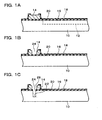
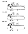
- Figs. 1A to Fig. 4B show a first embodiment of the method of manufacturing a semiconductor device to which the present invention is applied.
- a semiconductor substrate 10 is used.
- the semiconductor substrate 10 shown in Fig. 1A is a semiconductor wafer, but it may be a semiconductor chip.
- On the semiconductor substrate 10 is formed at least one (a plurality on a semiconductor wafer; one on a semiconductor chip) integrated circuit (for example, a circuit comprising transistors or memory) 12.
- On the semiconductor substrate 10 are formed a plurality of electrodes (for example, pads) 14.
- Each electrode 14 is electrically connected to the integrated circuit 12.
- the electrodes 14 may be formed of aluminum.
- the surface form of the electrodes 14 is not particularly restricted, but may be rectangular.
- passivation films 16 and 18, of a single layer or more layers are formed passivation films 16 and 18, of a single layer or more layers.
- the passivation films 16 and 18 can be formed of, for example, SiO 2 , SiN, polyimide resin, or the like.
- the electrodes 14, and interconnecting lines (not shown in the drawings) connecting the integrated circuit 12 and electrodes 14 are formed on the passivation film 16 .
- the other passivation film 18 is formed so as to avoid at least a part of the surface of the electrodes 14.
- a part may be etched to expose a part of the electrodes 14. For the etching, either dry etching or wet etching may be applied.
- the passivation film 18 the surface of the electrodes 14 may be etched.
- a depression 22 is formed from a first surface 20 thereof.
- the first surface 20 is the surface on which the electrodes 14 are formed.
- the depression 22 is formed to avoid the elements and interconnecting lines of the integrated circuit 12.
- a penetrating hole 24 may be formed in the electrodes 14.
- etching dry etching or wet etching
- the etching may be carried out after using a lithography process to form a patterned resist (not shown in the drawings).
- a penetrating hole 26 is also formed therein.
- the etchant used for etching the electrodes 14 may be replaced by a different etchant.
- a patterned resist (not shown in the drawings) may be formed by a lithography process.
- the depression 22 is formed in the semiconductor substrate 10 so as to communicate with the penetrating hole 24 (and penetrating hole 26).
- the penetrating hole 24 (and penetrating hole 26) and depression 22 can also be referred to collectively as a depression.
- etching dry etching or wet etching
- Etching may be carried out after forming a patterned resist (not shown in the drawings) by a lithography process.
- a laser for the formation of the depression 22, a laser (for example, a CO 2 laser, a YAG laser, or the like) may be used. The laser may be applied to the formation of the penetrating holes 24 and 26.
- the depression 22 and penetrating holes 24 and 26 may also be formed together by the use of a single etchant or laser.
- the insulating layer 28 may be an oxidation film.
- the insulating layer 28 may be of SiO 2 or SiN.
- the insulating layer 28 is formed on the inner wall of the depression 22.
- the insulating layer 28 may be formed on the bottom surface of the depression 22.
- the insulating layer 28 is formed so as not to fill in the depression 22. That is to say, a depression is formed by the insulating layer 28.
- the insulating layer 28 may be formed on the inner wall of the penetrating hole 26 in the passivation film 16.
- the insulating layer 28 may be formed over the passivation film 18.
- the insulating layer 28 may be formed on the inner wall of the penetrating hole 24 in the electrodes 14.
- the insulating layer 28 is formed to avoid a part of the electrodes 14 (for example, the top surface thereof).
- the insulating layer 28 may be formed to cover the whole surface of the electrodes 14, and then by partial etching (dry etching or wet etching), a part of the electrodes 14 exposed. The etching may be carried out after forming a patterned resist (not shown in the drawings) by a lithography process.
- a first conductive portion 30 is provided on the inside of the insulating layer 28, a first conductive portion 30 is provided.
- the first conductive portion 30 is formed of, for example, gold.
- the first conductive portion 30 may be of a material less easily oxidized than the second conductive portion 32 described below.
- the first conductive portion 30 may be provided only in the bottom of the depression 22 (or a depression formed by the insulating layer 28).
- the first conductive portion 30 may be formed by depositing the material thereof (for example, a solution including the material of which the first conductive portion 30 is constituted) in the depression 22 inkjet method. Since the insulating layer 28 is interposed between the inner surface of the depression 22 and the first conductive portion 30, electrical connection between the two is prevented.
- a second conductive portion 32 (See Fig. 3A) is provided, inside the insulating layer 28 and above the first conductive portion 30.
- the first and second conductive portions 30 and 32 may be electrically connected, and in intimate contact.
- the second conductive portion 32 is formed of a different material from the first conductive portion 30 (for example, copper, tungsten, or the like).
- a center portion 34 thereof may be formed as shown in Fig. 3A.
- the center portion 34 can be formed of any of copper, tungsten, doped polysilicon (for example, low temperature polysilicon).
- the outer layer 33 may include at least a barrier layer.
- the barrier layer prevents the material of the center portion 34 or of the seed layer described next from diffusing into the semiconductor substrate 10 (for example silicon).
- the barrier layer may be formed of a different material from the center portion 34 (for example, TiW, TiN, or TaN). If the center portion 34 is formed by electroplating, the outer layer 33 may include a seed layer. The seed layer is formed after forming the barrier layer. The seed layer is formed of the same material (for example copper) as the center portion 34. It should be noted that the second conductive portion 32 (at least the center portion 34 thereof) may be formed by electroless plating or an inkjet method.
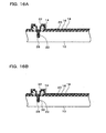
- first conductive portion 30 may, as described above, be formed after the insulating layer 28 is formed and before the outer layer 33 is formed, but equally the insulating layer 28 and outer layer 33 may be formed (See Fig. 16A), and thereafter the first conductive portion 30 may be formed (see Fig. 16B) .
- the second conductive portion 32 can be provided by forming the center portion 34 after the outer layer 33 is formed. A part of the second conductive portion 32 is positioned within the depression 22 in the semiconductor substrate 10. Between the inner surface of the depression 22 and the second conductive portion 32 is interposed the insulating layer 28, and therefore the two are electrically isolated. The second conductive portion 32 is electrically connected to the electrodes 14. For example, a portion of the electrodes 14 exposed from the insulating layer 28 may contact the second conductive portion 32.
- a part of the second conductive portion 32 may be positioned over the passivation film 18.
- the second conductive portion 32 may be provided only within the region of the electrodes 14.
- the second conductive portion 32 may project, at least above the depression 22.
- the second conductive portion 32 may project from the passivation film 18.
- the center portion 34 may be formed with the outer layer 33 remaining on the passivation film 18. In that case, since a layer continuous with the center portion 34 is formed over the passivation film 18, this layer is etched.
- solder layer 36 may be provided over the second conductive portion 32.
- the solder layer 36 may be formed of either of soft solder or hard solder.
- the solder layer 36 may be formed by covering regions other than the second conductive portion 32 with a resist.
- the first conductive portion 30 is exposed.
- the second surface 38 of the semiconductor substrate 10 may be removed.
- a part of the first conductive portion 30 may be removed.
- the second surface 38 may be etched in order that the first conductive portion 30 projects.
- etching SF 6 , CF 4 , or Cl 2 gas may be used.
- the etching may be carried out using a dry etching device.
- the first conductive portion 30 is formed of gold, it is difficult for the constituent molecules of the etching gas to adhere to the exposed surface, which is also not easily oxidized, and therefor the electrical connection is satisfactory.
- a reinforcing member of, for example, resin layer or resin tape may be provided on the first surface 20 of the semiconductor substrate 10.
- the first conductive portion 30 can be caused to project from the second surface 38 of the semiconductor substrate 10.
- the projecting first conductive portion 30 forms a projecting electrode.
- the first and second conductive portions 30 and 32 also form penetrating electrodes of the first and second surfaces 20 and 38.
- the exposed first conductive portion 30 is formed of a different material from the second conductive portion 32. Therefore, the material of the first and second conductive portions 30 and 32 can be selected considering the effect of being exposed, and cost and so on.
- concavities 22 may be formed corresponding to individual integrated circuits 12 (See Fig. 1A), and the semiconductor substrate 10 may be cut (for example, by dicing).
- a cutter for example, a dicer
- laser for example, a CO 2 laser, YAG laser, or the like
- a semiconductor device can be manufactured.
- the semiconductor device has electrodes 14 electrically connection to the integrated circuit 12 on the first surface 20, and has a semiconductor substrate in which the penetrating hole 22 is formed.
- the semiconductor device has the insulating layer 28 provided on the inner surface of the penetrating hole 22.
- the semiconductor device has first and second conductive portions 30 and 32 on the inside of the insulating layer 28, laminated in the thickness direction of the semiconductor substrate 10. Other components can be obtained according to the above described method.
- a plurality of semiconductor device manufactured by the above described method may be laminated, and electrical connection therebetween may be achieved through respective first conductive portions 30.
- This embodiment is effective for carrying out such a three-dimensional mounting.
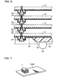
- the semiconductor device shown in Fig. 6 has a plurality of semiconductor substrates 10. In the direction of the first surface 20, the outermost positioned (in Fig. 6, the lowest) semiconductor substrate 10 has external terminals (for example, solder balls) 42.
- the external terminals 42 are provided on interconnecting lines 46 formed over a resin layer (for example, a stress relieving layer) 44.
- the interconnecting lines 46 are connected to the second conductive portion 32 on the first surface 20.
- a circuit board 1000 on which is mounted a semiconductor device 1, formed of a laminated plurality of semiconductor chips.
- the plurality of semiconductor chips is electrically connected by the above described first conductive portion 30.
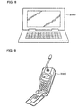
- Fig. 8 shows a notebook personal computer 2000
- Fig. 9 shows a mobile telephone 3000.
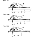
- Figs. 10A to 10C illustrate a second embodiment, being a modification of the process shown in Figs. 4A to 4B.
- the second surface of the semiconductor substrate 10 (the surface on the opposite side to the first surface 20) 38 is removed, for example by at least one method of mechanical polishing or cutting and chemical polishing or cutting. This process is carried out to a point before exposing the insulating layer 28 formed in the depression 22. It should be noted that the process shown in Fig. 10A may be omitted, and next the process in Fig. 10B carried out.
- the second surface 38 of the semiconductor substrate 10 is etched so that the insulating layer 28 is exposed.
- the second surface 38 of the semiconductor substrate 10 is etched so that the first conductive portion 30 projects while covered by the insulating layer 28.
- the etching is carried out with a first etchant whose properties are such as to yield a greater etching amount with respect to the semiconductor substrate (for example, a silicon base material) 10 than with respect to the insulating layer (for example, formed of SiO 2 ) 28.
- the first etchant may be SF 6 , CF 4 , or Cl 2 gas.
- the etching may be carried out using a dry etching device.
- first etchant may be a mixture of hydrofluoric acid and nitric acid, or a mixture of hydrofluoric acid, nitric acid, and acetic acid.
- the portion of the insulating layer 28 formed on the bottom surface of the depression 22 is etched. Then the first conductive portion 30 is exposed. The extreme surface of the first conductive portion 30 may be exposed, and the peripheral surface of the extremity of the first conductive portion 30 covered by the insulating layer 28.
- the outer layer 33 (for example, a barrier layer) of the first conductive portion 30 may also be etched. The etching may be carried out with a second etchant of characteristics such as to etch at least the insulating layer 28 without forming residues on the first conductive portion 30.
- a second etchant may be used an etchant which does not react (or has little reaction) with the material of the first conductive portion 30.
- the second etchant may be a mixture of argon and CF 4 gas, or a mixture of O 2 and CF 4 gas.
- the etching may be carried out using a dry etching device.
- the second etchant may be liquid hydrofluoric acid, or a liquid mixture of hydrofluoric acid and ammonium fluoride.
- the etching by the second etchant may have an etching rate with respect to the semiconductor substrate 10 which is slower than etching by the first etchant. According to this example, when the first conductive portion 30 is exposed from the insulating layer 28, no residues are left on the first conductive portion 30, and therefore a high quality penetrating electrode can be formed.
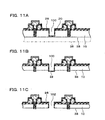
- Figs. 11A to 11C show the third embodiment of the method of manufacturing a semiconductor device to which the present invention is applied.
- a groove 100 is formed in the semiconductor substrate 10 (more precisely, in the first surface 20 thereof).
- the groove 100 is formed along the cutting line of the semiconductor substrate 10.
- the groove 100 may be formed by cutting, or may be formed by etching.
- the groove 100 may be formed in the step of forming the depression 22 shown in Fig. 1C, with the same process (for example, at the same time) as the depression 22.
- the insulating layer 28 may be provided within the groove 100.
- the groove 100 may be of substantially the same depth as the depression 22, or may be deeper than the depression 22, or may be more shallow than the depression 22.
- Figs. 11A to 11C show the components in the vicinity of the groove 100 when the respective steps shown in Figs. 10A to 10C are carried out.
- the process shown in Fig. 10A is carried out, and the second surface 38 of the semiconductor substrate 10 is polished to a point short of the insulating layer 28 (see Fig. 11A).
- the process shown in Fig. 10B is carried out, as shown in Fig. 11B, and the insulating layer 28 formed at the bottom of the groove 100 is caused to project from the second surface 38.
- the process shown in Fig. 10C is carried out, as shown in Fig. 11C, and by means of the second etchant, the insulating layer 28 formed at the bottom of the groove 100 is etched and removed. In this way, the bottom portion of the groove 100 is removed from the second surface, and the groove 100 becomes a slit 102. That is to say, the semiconductor substrate 100 is cut along the groove 100.
- the semiconductor substrate 10 can be cut simply. Since final cutting of the semiconductor substrate 10 is carried out by means of the second etchant, chipping is not likely to occur. Furthermore, in this embodiment, since the insulating layer 28 is formed within the groove 100, the semiconductor chip has the insulating layer 28 on the edge surface. Therefore, this semiconductor chip is not susceptible to edge shorting. Other details are as described in the first and second embodiments.
- Figs. 12A to 12B show the fourth embodiment of the method of manufacturing a semiconductor device to which the present invention is applied.
- the process of removing the bottom portion of the groove 100 is carried out with the material of the semiconductor substrate 10 exposed within the groove 100.
- the groove 100 may be formed, and in order that the insulating layer 28 is not attached, a resist or the like may be provided within the groove 100, or the insulating layer 28 which has entered the groove 100 may be removed.
- Other details are as described in the third embodiment.
- the process of Fig. 10B described in the second embodiment is carried out, and by means of the first etchant, the bottom portion of the groove 100 formed by a part of the semiconductor substrate 10 is etched and removed.
- the bottom portion of the groove 100 is removed from the second surface, and the groove 100 becomes the slit 102. That is to say, the semiconductor substrate 100 is cut along the groove 100.
- Other details are as described in the first, second, and third embodiments.
- Figs. 13A to 13B show the fifth embodiment of the method of manufacturing a semiconductor device to which the present invention is applied.
- a groove 110 is formed to be deeper than the depression 22.
- the groove 110 deeper than the depression 22 can be formed easily, exploiting the etching characteristics (the property of etching deeper in a wider spaces).
- the semiconductor substrate 100 is cut along the groove 110.
- the semiconductor substrate 10 is cut while the insulating layer 28 is formed within the groove 110, but the semiconductor substrate 10 may equally be cut while the material of the semiconductor substrate 10 is exposed within the groove 110.
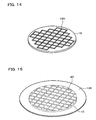
- Fig. 14 shows the sixth embodiment of the method of manufacturing a semiconductor device to which the present invention is applied.
- the content of this embodiment can be applied to any from the third to the fifth embodiments.
- a groove 120 is formed only in regions delineating a plurality of semiconductor chips having a plurality of integrated circuits 12 (See Fig. 1A). By this means, parts of the semiconductor substrate 10 that are not needed (for example, an outer peripheral portion) do not become separated, and damage to the semiconductor chip forming the product can be prevented.
- Fig. 15 shows the seventh embodiment of the method of manufacturing a semiconductor device to which the present invention is applied.
- the step of cutting the semiconductor substrate 10 is carried out after attaching a protective sheet 130 to the first surface 20 of the semiconductor substrate 10.
- the protective sheet 130 may be an adhesive tape or adhesive sheet.
- the present invention is not limited to the above-described embodiments, and various modifications can be made.
- the present invention includes various other configurations substantially the same as the configurations described in the embodiments (in function, method and effect, or in objective and effect, for example).
- the present invention also includes a configuration in which an unsubstantial portion in the described embodiments is replaced.
- the present invention also includes a configuration having the same effects as the configurations described in the embodiments, or a configuration able to achieve the same objective.
- the present invention includes a configuration in which a publicly known technique is added to the configurations in the embodiments.
Landscapes
- Internal Circuitry In Semiconductor Integrated Circuit Devices (AREA)
- Production Of Multi-Layered Print Wiring Board (AREA)
Abstract
Description
this method may further comprise cutting the semiconductor substrate.
the groove may be formed to be deeper than the depression; and
the bottom portion of the groove may be removed by the polishing of the second surface of the semiconductor substrate.
wherein the part of the insulating layer formed on the bottom portion of the groove may be etched and removed by means of the second etchant in the step (e2).
the step of removing the bottom portion of the groove-may be carried out in a state that a material of the semiconductor substrate is exposed within the groove.
the step of cutting the semiconductor substrate may be carried out with a protective sheet adhered to the first surface of the semiconductor substrate, so that a plurality of semiconductor chips obtained by cutting do not fall apart.
the groove may be formed only in regions sectioning the semiconductor substrate into a plurality of semiconductor chips having the plurality of integrated circuits.
wherein the first conductive portion is exposed from a second surface of the semiconductor substrate opposite to the first surface. According to the present invention, the exposed first conductive portion is formed of a different material from the second conductive portion. Therefore, materials of the first and second conductive portions can be selected bearing in mind the effect of the exposure, the cost, and so forth.
Claims (32)
- , A method of manufacturing a semiconductor device comprising:(a) forming a depression from a first surface of a semiconductor substrate in which an integrated circuit is formed;(b) providing an insulating layer on an inner surface of the depression;(c) providing a first conductive portion on the inside of the insulating layer;(d) forming a second conductive portion on the inside of the insulating layer and over the first conductive portion, being of a different material from the first conductive portion; and(e) exposing the first conductive portion from a second surface of the semiconductor substrate opposite to the first surface.
- The method of manufacturing a semiconductor device as defined in claim 1,
wherein the step (e) includes polishing the second surface of the semiconductor substrate. - The method of manufacturing a semiconductor device as defined in claim 1,
wherein the second surface is etched so that the first conductive portion projects in the step (e). - The method of manufacturing a semiconductor device as defined in claim 1, wherein:the first conductive portion is less easily oxidized than the second conductive portion.
- The method of manufacturing a semiconductor device as defined in claim 4,
wherein the first conductive portion is formed of gold, and at least a center portion of the second conductive portion is formed of copper. - The method of manufacturing a semiconductor device as defined in claim 1,
wherein the material of the first conductive portion is put in the depression by an inkjet method in the step (c). - The method of manufacturing a semiconductor device as defined in claim 1, wherein:the semiconductor substrate is a semiconductor wafer having a plurality of the integrated circuits, the depression being formed for each of the integrated circuits; andthe method further comprising cutting the semiconductor substrate.
- The method of manufacturing a semiconductor device as defined in claim 7,
wherein the step of cutting the semiconductor substrate includes:forming a groove in the first surface, along a cutting line of the semiconductor substrate; andremoving a bottom portion of the groove from the second surface so that the groove becomes a slit. - The method of manufacturing a semiconductor device as defined in claim 8,
wherein the groove is formed by cutting. - The method of manufacturing a semiconductor device as defined in claim 8,
wherein the groove is formed by etching. - The method of manufacturing a semiconductor device as defined in claim 8,
wherein the groove is formed in the same process as the depression in the step (a). - The method of manufacturing a semiconductor device as defined in claim 8, wherein:the step (e) includes polishing the second surface of the semiconductor substrate;the groove is formed to be deeper than the depression; andthe bottom portion of the groove is removed by the polishing of the second surface of the semiconductor substrate.
- The method of manufacturing a semiconductor device as defined in claim 8,
wherein the insulating layer is provided also on the inner surface of the groove in the step (b). - The method of manufacturing a semiconductor device as defined in claim 13,
wherein the step (e) includes:wherein part of the insulating layer formed on the bottom portion of the groove is caused to project from the second surface in the step (e1); and(e1) etching the second surface of the semiconductor substrate with a first etchant, having characteristics such that the etching amount with respect to the semiconductor substrate is greater than the etching amount with respect to the insulating layer, to cause the first conductive portion to project while covered by the insulating layer; and(e2) etching at least a part of the insulating layer formed on a bottom surface of the depression with a second etchant, having characteristics such that at least the insulating layer is etched without forming a residue on the first conductive portion, to expose the first conductive portion;
wherein the part of the insulating layer formed on the bottom portion of the groove is etched and removed by means of the second etchant in the step (e2). - The method of manufacturing a semiconductor device as defined in claim 8,
wherein the step of removing the bottom portion of the groove is carried out in a state that a material of the semiconductor substrate is exposed within the groove. - The method of manufacturing a semiconductor device as defined in claim 15,
wherein the step (e) includes:wherein the bottom portion of the groove formed by a part of the semiconductor substrate is etched and removed by means of the first etchant in the step (e1).(e1) etching the second surface of the semiconductor substrate with a first etchant, having characteristics such that the etching amount with respect to the semiconductor substrate is greater than the etching amount with respect to the insulating layer, to cause the first conductive portion to project while covered by the insulating layer; and(e2) etching at least a part of the insulating layer formed on a bottom surface of the depression with a second etchant, having characteristics such that at least the insulating layer is etched without forming a residue on the first conductive portion, to expose the first conductive portion; and - The method of manufacturing a semiconductor device as defined in claim 8,
wherein the step of cutting the semiconductor substrate is carried out with a protective sheet adhered to the first surface of the semiconductor substrate, so that a plurality of semiconductor chips obtained by cutting do not fall apart. - The method of manufacturing a semiconductor device as defined in claim 8,
wherein the groove is formed only in regions sectioning the semiconductor substrate into a plurality of semiconductor chips having the plurality of integrated circuits. - A method of manufacturing a semiconductor device, comprising:laminating a plurality of semiconductor devices manufactured by the method as defined in any of claims 1 to 18; andmaking electrical connections between the semiconductor devices through the conductive portions.
- A semiconductor device manufactured by the method as defined in any of claims 1 to 18.
- A semiconductor device manufactured by the method as defined in claim 19.
- A semiconductor device comprising:wherein the first and second conductive portions are formed of different materials; anda semiconductor substrate having an electrode which is electrically connected to an integrated circuit and provided on a first surface of the semiconductor substrate, and also having a penetrating hole;an insulating layer provided on an inner surface of the penetrating hole; andfirst and second conductive portions laminated on the inside of the insulating layer in the thickness direction of the semiconductor substrate,
wherein the first conductive portion is exposed from a second surface of the semiconductor substrate opposite to the first surface. - The semiconductor device as defined in claim 22,
wherein the first conductive portion projects from the second surface. - The semiconductor device as defined in claim 22,
wherein the first conductive portion is less easily oxidized than the second conductive portion. - The semiconductor device as defined in claim 24,
wherein the first conductive portion is formed of gold, and at least a center portion of the second conductive portion is formed of copper. - A semiconductor device comprising:wherein the semiconductor devices are laminated, and electrical connection between the semiconductor devices is achieved through the conductive portions.a plurality of the semiconductor devices as defined in claim 22,
- A circuit board on which is mounted the semiconductor device as defined in claim 20.
- A circuit board on which is mounted the semiconductor device as defined in claim 21.
- A circuit board on which is mounted the semiconductor device as defined in any of claims 22 to 26.
- An electronic instrument having the semiconductor device as defined in claim 20.
- An electronic instrument having the semiconductor device as defined in claim 21.
- An electronic instrument having the semiconductor device as defined in any of claims 22 to 26.
Applications Claiming Priority (5)
| Application Number | Priority Date | Filing Date | Title |
|---|---|---|---|
| JP2002076307 | 2002-03-19 | ||
| JP2002076307 | 2002-03-19 | ||
| JP2003007276 | 2003-01-15 | ||
| JP2003007276 | 2003-01-15 | ||
| PCT/JP2003/003301 WO2003079430A1 (en) | 2002-03-19 | 2003-03-19 | Semiconductor device and its manufacturing method, circuit board and electronic apparatus |
Publications (3)
| Publication Number | Publication Date |
|---|---|
| EP1391923A1 true EP1391923A1 (en) | 2004-02-25 |
| EP1391923A4 EP1391923A4 (en) | 2005-06-15 |
| EP1391923B1 EP1391923B1 (en) | 2012-05-09 |
Family
ID=28043774
Family Applications (1)
| Application Number | Title | Priority Date | Filing Date |
|---|---|---|---|
| EP03710424A Expired - Lifetime EP1391923B1 (en) | 2002-03-19 | 2003-03-19 | Manufacturing method of semiconductor device |
Country Status (8)
| Country | Link |
|---|---|
| US (1) | US6841849B2 (en) |
| EP (1) | EP1391923B1 (en) |
| JP (1) | JP4129643B2 (en) |
| KR (1) | KR100512817B1 (en) |
| CN (1) | CN1279605C (en) |
| AT (1) | ATE557419T1 (en) |
| TW (1) | TW594972B (en) |
| WO (1) | WO2003079430A1 (en) |
Cited By (1)
| Publication number | Priority date | Publication date | Assignee | Title |
|---|---|---|---|---|
| ITMI20081505A1 (en) * | 2008-08-08 | 2010-02-09 | Milano Politecnico | METHOD FOR BUMP FORMATION IN SUBSTRATES WITH THROUGH VIA |
Families Citing this family (34)
| Publication number | Priority date | Publication date | Assignee | Title |
|---|---|---|---|---|
| US6809421B1 (en) | 1996-12-02 | 2004-10-26 | Kabushiki Kaisha Toshiba | Multichip semiconductor device, chip therefor and method of formation thereof |
| JP4110390B2 (en) | 2002-03-19 | 2008-07-02 | セイコーエプソン株式会社 | Manufacturing method of semiconductor device |
| JP4081666B2 (en) * | 2002-09-24 | 2008-04-30 | セイコーエプソン株式会社 | Semiconductor device and manufacturing method thereof, circuit board, and electronic apparatus |
| JP2004297019A (en) * | 2003-03-28 | 2004-10-21 | Seiko Epson Corp | Semiconductor device, circuit board and electronic equipment |
| JP3646720B2 (en) * | 2003-06-19 | 2005-05-11 | セイコーエプソン株式会社 | Semiconductor device and manufacturing method thereof, circuit board, and electronic apparatus |
| JP3646719B2 (en) * | 2003-06-19 | 2005-05-11 | セイコーエプソン株式会社 | Semiconductor device and manufacturing method thereof, circuit board, and electronic apparatus |
| DE10342559B3 (en) * | 2003-09-15 | 2005-04-14 | Infineon Technologies Ag | Edge structure of power semiconductor component includes electrically- conducting layer deposited on parts of insulating layer in contact with region between conductivity types. |
| US8084866B2 (en) * | 2003-12-10 | 2011-12-27 | Micron Technology, Inc. | Microelectronic devices and methods for filling vias in microelectronic devices |
| JP4706180B2 (en) * | 2003-12-22 | 2011-06-22 | セイコーエプソン株式会社 | Manufacturing method of semiconductor device |
| JP3698160B2 (en) * | 2004-01-09 | 2005-09-21 | セイコーエプソン株式会社 | Manufacturing method of semiconductor device |
| US20050247894A1 (en) | 2004-05-05 | 2005-11-10 | Watkins Charles M | Systems and methods for forming apertures in microfeature workpieces |
| JP2005353682A (en) * | 2004-06-08 | 2005-12-22 | Seiko Epson Corp | Circuit element manufacturing method, electronic element manufacturing method, circuit board, electronic apparatus, and electro-optical device |
| US7232754B2 (en) | 2004-06-29 | 2007-06-19 | Micron Technology, Inc. | Microelectronic devices and methods for forming interconnects in microelectronic devices |
| SG120200A1 (en) | 2004-08-27 | 2006-03-28 | Micron Technology Inc | Slanted vias for electrical circuits on circuit boards and other substrates |
| US7300857B2 (en) | 2004-09-02 | 2007-11-27 | Micron Technology, Inc. | Through-wafer interconnects for photoimager and memory wafers |
| TWI250834B (en) * | 2004-11-03 | 2006-03-01 | Phoenix Prec Technology Corp | Method for fabricating electrical connections of circuit board |
| JP4170313B2 (en) * | 2005-05-24 | 2008-10-22 | シャープ株式会社 | Manufacturing method of semiconductor device |
| US7795134B2 (en) | 2005-06-28 | 2010-09-14 | Micron Technology, Inc. | Conductive interconnect structures and formation methods using supercritical fluids |
| US7622377B2 (en) * | 2005-09-01 | 2009-11-24 | Micron Technology, Inc. | Microfeature workpiece substrates having through-substrate vias, and associated methods of formation |
| US7262134B2 (en) | 2005-09-01 | 2007-08-28 | Micron Technology, Inc. | Microfeature workpieces and methods for forming interconnects in microfeature workpieces |
| US7863187B2 (en) * | 2005-09-01 | 2011-01-04 | Micron Technology, Inc. | Microfeature workpieces and methods for forming interconnects in microfeature workpieces |
| TWI293499B (en) | 2006-01-25 | 2008-02-11 | Advanced Semiconductor Eng | Three dimensional package and method of making the same |
| TWI287273B (en) * | 2006-01-25 | 2007-09-21 | Advanced Semiconductor Eng | Three dimensional package and method of making the same |
| KR101478810B1 (en) | 2006-07-28 | 2015-01-02 | 가부시키가이샤 한도오따이 에네루기 켄큐쇼 | Power storage device |
| US7629249B2 (en) | 2006-08-28 | 2009-12-08 | Micron Technology, Inc. | Microfeature workpieces having conductive interconnect structures formed by chemically reactive processes, and associated systems and methods |
| US7902643B2 (en) | 2006-08-31 | 2011-03-08 | Micron Technology, Inc. | Microfeature workpieces having interconnects and conductive backplanes, and associated systems and methods |
| JP2008166652A (en) * | 2007-01-05 | 2008-07-17 | Nippon Telegr & Teleph Corp <Ntt> | Manufacturing method of semiconductor device |
| JP4265668B2 (en) * | 2007-03-08 | 2009-05-20 | ソニー株式会社 | Circuit board manufacturing method and circuit board |
| JP4534096B2 (en) * | 2007-04-12 | 2010-09-01 | ローム株式会社 | Semiconductor chip, manufacturing method thereof, and semiconductor device |
| SG150410A1 (en) * | 2007-08-31 | 2009-03-30 | Micron Technology Inc | Partitioned through-layer via and associated systems and methods |
| US7884015B2 (en) | 2007-12-06 | 2011-02-08 | Micron Technology, Inc. | Methods for forming interconnects in microelectronic workpieces and microelectronic workpieces formed using such methods |
| KR101215648B1 (en) * | 2011-02-11 | 2012-12-26 | 에스케이하이닉스 주식회사 | Semiconductor chip and method for manufacturing the same |
| US20150262911A1 (en) * | 2014-03-14 | 2015-09-17 | International Business Machines Corporation | Tsv with end cap, method and 3d integrated circuit |
| US10804206B2 (en) * | 2017-07-31 | 2020-10-13 | Taiwan Semiconductor Manufacturing Co., Ltd. | Deep trench protection |
Family Cites Families (12)
| Publication number | Priority date | Publication date | Assignee | Title |
|---|---|---|---|---|
| US117705A (en) * | 1871-08-01 | Improvement in machines for removing runners from strawberry vines | ||
| JPS607149A (en) * | 1983-06-24 | 1985-01-14 | Nec Corp | Manufacture of semiconductor device |
| JPS607148A (en) * | 1983-06-24 | 1985-01-14 | Nec Corp | Manufacture of semiconductor device |
| JPH0215652A (en) * | 1988-07-01 | 1990-01-19 | Mitsubishi Electric Corp | Semiconductor device and manufacture thereof |
| US4978639A (en) * | 1989-01-10 | 1990-12-18 | Avantek, Inc. | Method for the simultaneous formation of via-holes and wraparound plating on semiconductor chips |
| DE4314907C1 (en) * | 1993-05-05 | 1994-08-25 | Siemens Ag | Method for producing semiconductor components making electrically conducting contact with one another vertically |
| JP3537447B2 (en) | 1996-10-29 | 2004-06-14 | トル‐シ・テクノロジーズ・インコーポレイテッド | Integrated circuit and manufacturing method thereof |
| JP3184493B2 (en) * | 1997-10-01 | 2001-07-09 | 松下電子工業株式会社 | Electronic device manufacturing method |
| JP3792954B2 (en) * | 1999-08-10 | 2006-07-05 | 株式会社東芝 | Manufacturing method of semiconductor device |
| US6322903B1 (en) | 1999-12-06 | 2001-11-27 | Tru-Si Technologies, Inc. | Package of integrated circuits and vertical integration |
| JP3778256B2 (en) * | 2000-02-28 | 2006-05-24 | セイコーエプソン株式会社 | Semiconductor device and manufacturing method thereof, circuit board, and electronic apparatus |
| JP2001326325A (en) * | 2000-05-16 | 2001-11-22 | Seiko Epson Corp | Semiconductor device and manufacturing method thereof |
-
2003
- 2003-03-19 CN CNB03800707XA patent/CN1279605C/en not_active Expired - Lifetime
- 2003-03-19 WO PCT/JP2003/003301 patent/WO2003079430A1/en not_active Ceased
- 2003-03-19 KR KR10-2003-7015901A patent/KR100512817B1/en not_active Expired - Lifetime
- 2003-03-19 JP JP2003577327A patent/JP4129643B2/en not_active Expired - Lifetime
- 2003-03-19 AT AT03710424T patent/ATE557419T1/en active
- 2003-03-19 TW TW092106052A patent/TW594972B/en not_active IP Right Cessation
- 2003-03-19 EP EP03710424A patent/EP1391923B1/en not_active Expired - Lifetime
- 2003-11-10 US US10/703,570 patent/US6841849B2/en not_active Expired - Lifetime
Cited By (3)
| Publication number | Priority date | Publication date | Assignee | Title |
|---|---|---|---|---|
| ITMI20081505A1 (en) * | 2008-08-08 | 2010-02-09 | Milano Politecnico | METHOD FOR BUMP FORMATION IN SUBSTRATES WITH THROUGH VIA |
| US8759215B2 (en) | 2008-08-08 | 2014-06-24 | Stmicroelectronics S.R.L. | Method for forming bumps in substrates with through vias |
| US8928123B2 (en) | 2008-08-08 | 2015-01-06 | Stmicroelectronics S.R.L. | Through via structure including a conductive portion and aligned solder portion |
Also Published As
| Publication number | Publication date |
|---|---|
| KR100512817B1 (en) | 2005-09-06 |
| KR20040012897A (en) | 2004-02-11 |
| EP1391923A4 (en) | 2005-06-15 |
| TW200305992A (en) | 2003-11-01 |
| ATE557419T1 (en) | 2012-05-15 |
| US6841849B2 (en) | 2005-01-11 |
| EP1391923B1 (en) | 2012-05-09 |
| TW594972B (en) | 2004-06-21 |
| US20040155330A1 (en) | 2004-08-12 |
| WO2003079430A1 (en) | 2003-09-25 |
| CN1533604A (en) | 2004-09-29 |
| JPWO2003079430A1 (en) | 2005-07-21 |
| JP4129643B2 (en) | 2008-08-06 |
| CN1279605C (en) | 2006-10-11 |
Similar Documents
| Publication | Publication Date | Title |
|---|---|---|
| US6841849B2 (en) | Semiconductor device and method of manufacturing the same, circuit board and electronic instrument | |
| US7029937B2 (en) | Semiconductor device and method of manufacturing the same, circuit board, and electronic instrument | |
| JP3918935B2 (en) | Manufacturing method of semiconductor device | |
| CN100367452C (en) | Semiconductor device and manufacturing method thereof | |
| US6566232B1 (en) | Method of fabricating semiconductor device | |
| JP3972846B2 (en) | Manufacturing method of semiconductor device | |
| KR100641696B1 (en) | Method of manufacturing semiconductor device | |
| US8309860B2 (en) | Electronic component built-in substrate and method of manufacturing the same | |
| JP3690407B2 (en) | Manufacturing method of semiconductor device | |
| US20090093117A1 (en) | Method of manufacturing substrate | |
| US20040192033A1 (en) | Semiconductor device, method of manufacturing the same, circuit board, and electronic instrument | |
| KR20040092435A (en) | Semiconductor device and manufacturing method thereof | |
| US8129835B2 (en) | Package substrate having semiconductor component embedded therein and fabrication method thereof | |
| EP1478021B1 (en) | Semiconductor device and manufacturing method thereof | |
| US7193297B2 (en) | Semiconductor device, method for manufacturing the same, circuit substrate and electronic device | |
| JP3523815B2 (en) | Semiconductor device | |
| US7375007B2 (en) | Method of manufacturing a semiconductor device | |
| JP4536629B2 (en) | Manufacturing method of semiconductor chip | |
| JP2004221351A (en) | Semiconductor device and its manufacturing method, circuit board, and electronic equipment | |
| JP2004221350A (en) | Semiconductor chip, semiconductor wafer, semiconductor device and manufacturing method thereof, circuit board, and electronic equipment |
Legal Events
| Date | Code | Title | Description |
|---|---|---|---|
| PUAI | Public reference made under article 153(3) epc to a published international application that has entered the european phase |
Free format text: ORIGINAL CODE: 0009012 |
|
| 17P | Request for examination filed |
Effective date: 20031127 |
|
| AK | Designated contracting states |
Kind code of ref document: A1 Designated state(s): AT BE BG CH CY CZ DE DK EE ES FI FR GB GR HU IE IT LI LU MC NL PT RO SE SI SK TR |
|
| A4 | Supplementary search report drawn up and despatched |
Effective date: 20050502 |
|
| GRAP | Despatch of communication of intention to grant a patent |
Free format text: ORIGINAL CODE: EPIDOSNIGR1 |
|
| RTI1 | Title (correction) |
Free format text: MANUFACTURING METHOD OF SEMICONDUCTOR DEVICE |
|
| GRAS | Grant fee paid |
Free format text: ORIGINAL CODE: EPIDOSNIGR3 |
|
| GRAA | (expected) grant |
Free format text: ORIGINAL CODE: 0009210 |
|
| AK | Designated contracting states |
Kind code of ref document: B1 Designated state(s): AT BE BG CH CY CZ DE DK EE ES FI FR GB GR HU IE IT LI LU MC NL PT RO SE SI SK TR |
|
| REG | Reference to a national code |
Ref country code: GB Ref legal event code: FG4D |
|
| REG | Reference to a national code |
Ref country code: CH Ref legal event code: EP Ref country code: AT Ref legal event code: REF Ref document number: 557419 Country of ref document: AT Kind code of ref document: T Effective date: 20120515 |
|
| REG | Reference to a national code |
Ref country code: IE Ref legal event code: FG4D |
|
| REG | Reference to a national code |
Ref country code: DE Ref legal event code: R096 Ref document number: 60340882 Country of ref document: DE Effective date: 20120705 |
|
| REG | Reference to a national code |
Ref country code: NL Ref legal event code: VDEP Effective date: 20120509 |
|
| PG25 | Lapsed in a contracting state [announced via postgrant information from national office to epo] |
Ref country code: CY Free format text: LAPSE BECAUSE OF FAILURE TO SUBMIT A TRANSLATION OF THE DESCRIPTION OR TO PAY THE FEE WITHIN THE PRESCRIBED TIME-LIMIT Effective date: 20120509 Ref country code: SE Free format text: LAPSE BECAUSE OF FAILURE TO SUBMIT A TRANSLATION OF THE DESCRIPTION OR TO PAY THE FEE WITHIN THE PRESCRIBED TIME-LIMIT Effective date: 20120509 Ref country code: FI Free format text: LAPSE BECAUSE OF FAILURE TO SUBMIT A TRANSLATION OF THE DESCRIPTION OR TO PAY THE FEE WITHIN THE PRESCRIBED TIME-LIMIT Effective date: 20120509 |
|
| REG | Reference to a national code |
Ref country code: AT Ref legal event code: MK05 Ref document number: 557419 Country of ref document: AT Kind code of ref document: T Effective date: 20120509 |
|
| PG25 | Lapsed in a contracting state [announced via postgrant information from national office to epo] |
Ref country code: SI Free format text: LAPSE BECAUSE OF FAILURE TO SUBMIT A TRANSLATION OF THE DESCRIPTION OR TO PAY THE FEE WITHIN THE PRESCRIBED TIME-LIMIT Effective date: 20120509 Ref country code: PT Free format text: LAPSE BECAUSE OF FAILURE TO SUBMIT A TRANSLATION OF THE DESCRIPTION OR TO PAY THE FEE WITHIN THE PRESCRIBED TIME-LIMIT Effective date: 20120910 Ref country code: GR Free format text: LAPSE BECAUSE OF FAILURE TO SUBMIT A TRANSLATION OF THE DESCRIPTION OR TO PAY THE FEE WITHIN THE PRESCRIBED TIME-LIMIT Effective date: 20120810 |
|
| PG25 | Lapsed in a contracting state [announced via postgrant information from national office to epo] |
Ref country code: BE Free format text: LAPSE BECAUSE OF FAILURE TO SUBMIT A TRANSLATION OF THE DESCRIPTION OR TO PAY THE FEE WITHIN THE PRESCRIBED TIME-LIMIT Effective date: 20120509 |
|
| PG25 | Lapsed in a contracting state [announced via postgrant information from national office to epo] |
Ref country code: AT Free format text: LAPSE BECAUSE OF FAILURE TO SUBMIT A TRANSLATION OF THE DESCRIPTION OR TO PAY THE FEE WITHIN THE PRESCRIBED TIME-LIMIT Effective date: 20120509 Ref country code: DK Free format text: LAPSE BECAUSE OF FAILURE TO SUBMIT A TRANSLATION OF THE DESCRIPTION OR TO PAY THE FEE WITHIN THE PRESCRIBED TIME-LIMIT Effective date: 20120509 Ref country code: SK Free format text: LAPSE BECAUSE OF FAILURE TO SUBMIT A TRANSLATION OF THE DESCRIPTION OR TO PAY THE FEE WITHIN THE PRESCRIBED TIME-LIMIT Effective date: 20120509 Ref country code: RO Free format text: LAPSE BECAUSE OF FAILURE TO SUBMIT A TRANSLATION OF THE DESCRIPTION OR TO PAY THE FEE WITHIN THE PRESCRIBED TIME-LIMIT Effective date: 20120509 Ref country code: CZ Free format text: LAPSE BECAUSE OF FAILURE TO SUBMIT A TRANSLATION OF THE DESCRIPTION OR TO PAY THE FEE WITHIN THE PRESCRIBED TIME-LIMIT Effective date: 20120509 Ref country code: EE Free format text: LAPSE BECAUSE OF FAILURE TO SUBMIT A TRANSLATION OF THE DESCRIPTION OR TO PAY THE FEE WITHIN THE PRESCRIBED TIME-LIMIT Effective date: 20120509 Ref country code: NL Free format text: LAPSE BECAUSE OF FAILURE TO SUBMIT A TRANSLATION OF THE DESCRIPTION OR TO PAY THE FEE WITHIN THE PRESCRIBED TIME-LIMIT Effective date: 20120509 |
|
| PG25 | Lapsed in a contracting state [announced via postgrant information from national office to epo] |
Ref country code: IT Free format text: LAPSE BECAUSE OF FAILURE TO SUBMIT A TRANSLATION OF THE DESCRIPTION OR TO PAY THE FEE WITHIN THE PRESCRIBED TIME-LIMIT Effective date: 20120509 |
|
| PLBE | No opposition filed within time limit |
Free format text: ORIGINAL CODE: 0009261 |
|
| STAA | Information on the status of an ep patent application or granted ep patent |
Free format text: STATUS: NO OPPOSITION FILED WITHIN TIME LIMIT |
|
| 26N | No opposition filed |
Effective date: 20130212 |
|
| PG25 | Lapsed in a contracting state [announced via postgrant information from national office to epo] |
Ref country code: ES Free format text: LAPSE BECAUSE OF FAILURE TO SUBMIT A TRANSLATION OF THE DESCRIPTION OR TO PAY THE FEE WITHIN THE PRESCRIBED TIME-LIMIT Effective date: 20120820 |
|
| REG | Reference to a national code |
Ref country code: DE Ref legal event code: R097 Ref document number: 60340882 Country of ref document: DE Effective date: 20130212 |
|
| PG25 | Lapsed in a contracting state [announced via postgrant information from national office to epo] |
Ref country code: BG Free format text: LAPSE BECAUSE OF FAILURE TO SUBMIT A TRANSLATION OF THE DESCRIPTION OR TO PAY THE FEE WITHIN THE PRESCRIBED TIME-LIMIT Effective date: 20120809 |
|
| PG25 | Lapsed in a contracting state [announced via postgrant information from national office to epo] |
Ref country code: MC Free format text: LAPSE BECAUSE OF NON-PAYMENT OF DUE FEES Effective date: 20130331 |
|
| REG | Reference to a national code |
Ref country code: CH Ref legal event code: PL |
|
| REG | Reference to a national code |
Ref country code: IE Ref legal event code: MM4A |
|
| PG25 | Lapsed in a contracting state [announced via postgrant information from national office to epo] |
Ref country code: LI Free format text: LAPSE BECAUSE OF NON-PAYMENT OF DUE FEES Effective date: 20130331 Ref country code: IE Free format text: LAPSE BECAUSE OF NON-PAYMENT OF DUE FEES Effective date: 20130319 Ref country code: CH Free format text: LAPSE BECAUSE OF NON-PAYMENT OF DUE FEES Effective date: 20130331 |
|
| PG25 | Lapsed in a contracting state [announced via postgrant information from national office to epo] |
Ref country code: TR Free format text: LAPSE BECAUSE OF FAILURE TO SUBMIT A TRANSLATION OF THE DESCRIPTION OR TO PAY THE FEE WITHIN THE PRESCRIBED TIME-LIMIT Effective date: 20120509 |
|
| PG25 | Lapsed in a contracting state [announced via postgrant information from national office to epo] |
Ref country code: HU Free format text: LAPSE BECAUSE OF FAILURE TO SUBMIT A TRANSLATION OF THE DESCRIPTION OR TO PAY THE FEE WITHIN THE PRESCRIBED TIME-LIMIT; INVALID AB INITIO Effective date: 20030319 Ref country code: LU Free format text: LAPSE BECAUSE OF NON-PAYMENT OF DUE FEES Effective date: 20130319 |
|
| REG | Reference to a national code |
Ref country code: FR Ref legal event code: PLFP Year of fee payment: 14 |
|
| REG | Reference to a national code |
Ref country code: FR Ref legal event code: PLFP Year of fee payment: 15 |
|
| REG | Reference to a national code |
Ref country code: FR Ref legal event code: PLFP Year of fee payment: 16 |
|
| REG | Reference to a national code |
Ref country code: DE Ref legal event code: R082 Ref document number: 60340882 Country of ref document: DE Representative=s name: MERH-IP MATIAS ERNY REICHL HOFFMANN PATENTANWA, DE |
|
| PGFP | Annual fee paid to national office [announced via postgrant information from national office to epo] |
Ref country code: GB Payment date: 20220321 Year of fee payment: 20 Ref country code: DE Payment date: 20220322 Year of fee payment: 20 |
|
| PGFP | Annual fee paid to national office [announced via postgrant information from national office to epo] |
Ref country code: FR Payment date: 20220322 Year of fee payment: 20 |
|
| REG | Reference to a national code |
Ref country code: DE Ref legal event code: R071 Ref document number: 60340882 Country of ref document: DE |
|
| REG | Reference to a national code |
Ref country code: GB Ref legal event code: PE20 Expiry date: 20230318 |
|
| PG25 | Lapsed in a contracting state [announced via postgrant information from national office to epo] |
Ref country code: GB Free format text: LAPSE BECAUSE OF EXPIRATION OF PROTECTION Effective date: 20230318 |