JP4536629B2 - Manufacturing method of semiconductor chip - Google Patents
Manufacturing method of semiconductor chip Download PDFInfo
- Publication number
- JP4536629B2 JP4536629B2 JP2005274242A JP2005274242A JP4536629B2 JP 4536629 B2 JP4536629 B2 JP 4536629B2 JP 2005274242 A JP2005274242 A JP 2005274242A JP 2005274242 A JP2005274242 A JP 2005274242A JP 4536629 B2 JP4536629 B2 JP 4536629B2
- Authority
- JP
- Japan
- Prior art keywords
- insulating film
- film
- opening
- semiconductor chip
- hole
- Prior art date
- Legal status (The legal status is an assumption and is not a legal conclusion. Google has not performed a legal analysis and makes no representation as to the accuracy of the status listed.)
- Active
Links
Images


Classifications
-
- H—ELECTRICITY
- H01—ELECTRIC ELEMENTS
- H01L—SEMICONDUCTOR DEVICES NOT COVERED BY CLASS H10
- H01L21/00—Processes or apparatus adapted for the manufacture or treatment of semiconductor or solid state devices or of parts thereof
- H01L21/70—Manufacture or treatment of devices consisting of a plurality of solid state components formed in or on a common substrate or of parts thereof; Manufacture of integrated circuit devices or of parts thereof
- H01L21/71—Manufacture of specific parts of devices defined in group H01L21/70
- H01L21/768—Applying interconnections to be used for carrying current between separate components within a device comprising conductors and dielectrics
- H01L21/76898—Applying interconnections to be used for carrying current between separate components within a device comprising conductors and dielectrics formed through a semiconductor substrate
-
- H—ELECTRICITY
- H01—ELECTRIC ELEMENTS
- H01L—SEMICONDUCTOR DEVICES NOT COVERED BY CLASS H10
- H01L23/00—Details of semiconductor or other solid state devices
- H01L23/48—Arrangements for conducting electric current to or from the solid state body in operation, e.g. leads, terminal arrangements ; Selection of materials therefor
Description
本発明は、半導体チップの製造方法に係り、特に電極パッドと電気的に接続される貫通ビアを備えた半導体チップの製造方法に関する。 The present invention relates to a method for manufacturing a semiconductor chip, and more particularly to a method for manufacturing a semiconductor chip having a through via electrically connected to an electrode pad.
近年の電子機器の高性能化や小型化に伴って、複数の半導体チップを積層させたマルチチップパーケージの開発が行なわれている。マルチチップパーケージに適用される半導体チップは、上下方向に配置された他の半導体チップと電気的に接続するための貫通ビアを有する。 In recent years, multi-chip packages in which a plurality of semiconductor chips are stacked are being developed along with improvement in performance and miniaturization of electronic devices. A semiconductor chip applied to the multi-chip package has a through via for electrically connecting to another semiconductor chip arranged in the vertical direction.
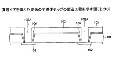
図1は、貫通ビアを備えた従来の半導体チップの断面図である。 FIG. 1 is a cross-sectional view of a conventional semiconductor chip having a through via.
図1に示すように、半導体チップ100は、半導体基板101と、図示していない半導体素子と、電極パッド102と、絶縁膜103と、貫通ビア105とを有する。半導体基板101には、半導体基板101を貫通し、電極パッド102を露出する貫通孔106が形成されている。半導体素子(図示せず)は、半導体基板101の第1の主面101A側に設けられている。電極パッド102は、半導体基板101の第1の主面101A側に設けられており、図示していない配線により半導体素子と電気的に接続されている。絶縁膜103は、貫通孔106の側壁と半導体基板101の第2の主面101B(非能動面)とを覆うように設けられている。貫通ビア105は、貫通孔106に設けられており、電極パッド102と電気的に接続されている。
As shown in FIG. 1, the
図2〜図5は、貫通ビアを備えた従来の半導体チップの製造工程を示す図である。図2〜図5において、図1に示した半導体チップ100と同一構成部分には同一符号を付す。
2 to 5 are views showing a manufacturing process of a conventional semiconductor chip having a through via. 2 to 5, the same components as those of the
図2〜図5を参照して、半導体チップ100の製造方法について説明する。図2に示すように、公知の方法により、半導体基板101の第1の主面101Aに図示していない半導体素子及び配線と、電極パッド102とを形成する。その後、半導体基板101の第2の主面101B側からウエットエッチング法により半導体基板101をエッチングして、電極パッド102を露出する貫通孔106を形成する。
A method for manufacturing the
次いで、図3に示すように、図2に示した構造体の上面を覆うように絶縁膜103を形成し、続いて、絶縁膜103上に、電極パッド102に設けられた絶縁膜103を露出する開口部108Aを有したレジスト膜108を形成する。
Next, as shown in FIG. 3, an
次いで、図4に示すように、レジスト膜108をマスクとして、エッチング法により電極パッド102に設けられた絶縁膜103を除去する。エッチング法としては、ドライエッチング法またはウエットエッチング法を用いる。
Next, as shown in FIG. 4, the
次いで、図5に示すように、レジスト膜108を除去して、印刷法により貫通孔106にはんだペーストを充填して、貫通ビア105を形成する。これにより、半導体チップ100が製造される(例えば、特許文献1参照。)。
しかしながら、ウエットエッチング法を用いて、電極パッド102に設けられた絶縁膜103を除去する場合、オーバーエッチング量によっては半導体基板101の側壁に形成された必要な絶縁膜103も除去されてしまうため、半導体チップ100の歩留まりが低下してしまうという問題があった。
However, when the
また、ドライエッチング法を用いて、電極パッド102に設けられた絶縁膜103を除去する場合、オーバーエッチング量によっては電極パッド102が損傷してしまうため、半導体チップ100の歩留まりが低下してしまうという問題があった。
In addition, when the
そこで本発明は、上述した問題点に鑑みなされたものであり、歩留まりを向上させることのできる半導体チップの製造方法を提供することを目的とする。 Therefore, the present invention has been made in view of the above-described problems, and an object of the present invention is to provide a semiconductor chip manufacturing method capable of improving the yield.
本発明の一観点によれば、半導体基板に形成された半導体素子と電気的に接続された電極パッドと、該電極パッドと電気的に接続された貫通ビアとを備えた半導体チップの製造方法であって、前記電極パッド上に第1開口部を有した第1のレジスト膜を形成する第1レジスト膜形成工程と、前記第1開口部及び前記第1のレジスト膜を覆うように金属膜を形成する金属膜形成工程と、前記第1開口部の形成位置に、前記第1開口部よりも直径の小さい第2開口部を有する第2のレジスト膜を、前記金属膜を覆うように形成する第2レジスト膜形成工程と、前記金属膜、前記半導体基板及び電極パッドを貫通し、前記第2開口部の形成位置に対応する貫通孔を形成する貫通孔形成工程と、前記第1開口部の上端部を覆うように絶縁膜除去用テープを設ける絶縁膜除去用テープ貼付工程と、前記絶縁膜除去用テープ貼付工程後に、前記半導体基板の前記半導体素子の面と反対側の面側から、前記貫通孔の側壁及び前記第1開口部に前記絶縁膜を形成する絶縁膜形成工程と、前記絶縁膜形成工程の後に前記絶縁膜除去用テープを除去する絶縁膜除去用テープ除去工程と、前記絶縁膜除去用テープ除去工程の後に、前記貫通孔及び前記第1開口部に前記貫通ビアを形成する貫通ビア形成工程とを含むことを特徴とする半導体チップの製造方法が提供される。 According to one aspect of the present invention, there is provided a semiconductor chip manufacturing method including an electrode pad electrically connected to a semiconductor element formed on a semiconductor substrate, and a through via electrically connected to the electrode pad. there are a first resist film forming step of forming a first resist film having a first opening on the electrode pad, a metallic film so as to cover the first opening and the first resist film A second resist film having a second opening having a diameter smaller than that of the first opening is formed so as to cover the metal film at a formation position of the metal film to be formed and a position where the first opening is formed. A second resist film forming step, a through hole forming step of penetrating the metal film, the semiconductor substrate and the electrode pad to form a through hole corresponding to the formation position of the second opening , and the first opening tape insulation film removing so as to cover the upper portion And insulation film removing tape pasting step of providing a, after the insulation film removing tape pasting step, from the side of the surface opposite of the semiconductor device of the semiconductor substrate, the sidewalls and the first opening of the through hole The insulating film forming step for forming the insulating film, the insulating film removing tape removing step for removing the insulating film removing tape after the insulating film forming step, and the penetrating after the insulating film removing tape removing step. And a through via forming step of forming the through via in the hole and the first opening .
本発明によれば、レジスト膜上に開口部を覆う絶縁膜除去用テープを貼り付け、貫通孔の側壁及び前記第1開口部に絶縁膜を形成することで、第1開口部よりも直径の小さい貫通孔と第1開口部とにより構成される段差部分の絶縁膜の厚さを貫通孔に形成される絶縁膜よりも薄くすることが可能となる。これにより、絶縁膜除去用テープを除去する際、絶縁膜を段差部分で破断させて、貫通孔の側壁を絶縁膜で精度良く覆うことが可能となるため、半導体チップの歩留まりを向上させることができる。 According to the present invention, paste the insulation film removing tape covering the opening portion on the resist film, by forming the insulating film on the side wall and the first opening of the transmural hole diameter than the first opening It is possible to make the thickness of the insulating film in the step portion constituted by the small through hole and the first opening portion thinner than the insulating film formed in the through hole. As a result, when removing the insulating film removing tape, it is possible to break the insulating film at the step portion and accurately cover the side wall of the through hole with the insulating film, so that the yield of the semiconductor chip can be improved. it can.
本発明によれば、電極パッドと電気的に接続される貫通ビアを備えた半導体チップの歩留まりを向上させることができる。 According to the present invention, it is possible to improve the yield of a semiconductor chip provided with a through via electrically connected to an electrode pad.
次に、図面に基づいて本発明の実施の形態について説明する。 Next, embodiments of the present invention will be described with reference to the drawings.
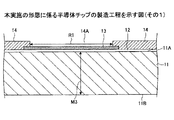
図6は、本発明の実施の形態に係る半導体チップの断面図である。 FIG. 6 is a cross-sectional view of a semiconductor chip according to an embodiment of the present invention.
図6を参照するに、半導体チップ10は、半導体基板11と、半導体素子(図示せず)と、絶縁膜12,17と、電極パッド13と、保護膜14と、導電部材16と、貫通ビア18とを有する。
Referring to FIG. 6, a
半導体基板11は、薄板化されており、貫通ビア18を配設するための貫通孔21が形成されている。貫通孔21は、半導体基板11、絶縁膜12、及び電極パッド13を貫通している。半導体基板11の材料としては、例えば、シリコンや、GaAs等の化合物半導体を用いることができる。薄板化された半導体基板11の厚さM1は、例えば、200μmとすることができる。
The
半導体素子(図示せず)は、トランジスタ等の素子であり、半導体基板11の第1の主面11A側に設けられている。半導体素子は、図示していない配線を介して電極パッド13と電気的に接続されている。
The semiconductor element (not shown) is an element such as a transistor, and is provided on the first
絶縁膜12は、半導体基板11の第1の主面11Aを覆うように設けられている。絶縁膜12は、半導体基板11と電極パッド13との間を絶縁する膜である。絶縁膜12は、例えば、CVD法により形成できる。絶縁膜12としては、例えば、SiO2膜やSiN膜を用いることができる。絶縁膜12の厚さは、例えば、0.1μmとすることができる。
The
電極パッド13は、絶縁膜12上に設けられている。電極パッド13は、図示していない配線により半導体素子(図示せず)と電気的に接続されている。電極パッド13の材料としては、例えば、Alを用いることができる。また、電極パッド13は、例えば、スパッタ法により絶縁膜12上にAl膜を形成し、このAl膜をドライエッチング法によりパターニングすることで形成できる。
The
保護膜14は、絶縁膜12を覆うように設けられており、電極パッド13を露出する開口部14Aを有する。開口部14Aの直径は、例えば、120μmとすることができる。保護膜14は、例えば、CVD法により形成することができる。保護膜14としては、例えば、SiO2膜、SiO2膜とSiN膜との積層膜等を用いることができる。
The
導電部材16は、貫通ビア18の突出部24と電極パッド13との間に設けられており、突出部24の下面24Aと電極パッド13の上面13Aとに接触している。導電部材16は、貫通ビア18の突出部24と電極パッド13とを電気的に接続するためのものである。導電部材16は、例えば、スパッタ法、CVD法、無電解めっき法等により形成することができる。導電部材16の材料としては、導電金属を用いることができ、具体的には、例えば、Ti膜とCu膜とを順次積層させたTi/Cu積層膜や、Cr膜とCu膜とを順次積層させたCr/Cu積層膜等を用いることができる。
The
絶縁膜17は、半導体基板11の第2の主面11B上と、貫通孔21の側壁と、導電部材16と貫通ビア18との間とに設けられている。絶縁膜17は、半導体基板11と貫通ビア18との間を絶縁するための膜である。絶縁膜17は、例えば、CVD法により形成することができる。絶縁膜17としては、例えば、SiO2膜やSiN膜等を用いることができる。また、絶縁膜17の厚さM2は、例えば、1μmとすることができる。
The
貫通ビア18は、貫通部23と、突出部24とを有する。貫通部23は、絶縁膜17が形成された貫通孔21に設けられている。貫通部23の上端部には、突出部24が一体的に設けられている。また、半導体チップ10の上下方向に他の半導体チップを積層させて、マルチチップパーケージを構成する場合、貫通部23の下端部23Aには、他の半導体チップの貫通ビア(図示せず)が電気的に接続される。
The through via 18 has a through
突出部24は、導電部材16上と、電極パッド13よりも上方に位置する絶縁膜17上とに設けられている。突出部24は、貫通部23よりも幅広形状とされている。また、突出部24の上端部(導電部材16上に位置する突出部24部分)は、貫通部23の近傍に位置する突出部24部分よりもさらに幅広形状とされている。半導体チップ10の上下方向に他の半導体チップを積層させて、マルチチップパーケージを構成する場合、突出部24には、他の半導体チップの貫通ビア(図示せず)が電気的に接続される。
The protruding
貫通ビア18は、例えば、めっき法により形成することができる。貫通ビア18の材料としては、導電金属を用いることができ、具体的には、例えば、Cuを用いることができる。また、突出部24を形成する際、導電部材16を給電層とすることができる。
The through via 18 can be formed by, for example, a plating method. As a material of the through via 18, a conductive metal can be used, and specifically, for example, Cu can be used. Moreover, when forming the
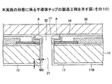
図7〜図19は、本実施の形態に係る半導体チップの製造工程を示す図である。図7〜図19において、先の図6で説明した半導体チップ10と同一構成部分には同一符号を付す。
7 to 19 are views showing a manufacturing process of the semiconductor chip according to the present embodiment. 7 to 19, the same components as those of the
図7〜図19を参照して、本実施の形態に係る半導体チップ10の製造方法について説明する。
A method for manufacturing the
始めに、図7に示すように、薄板化される前の半導体基板11の第1の主面11Aに、公知の技術により半導体素子(図示せず)を形成し、次いで、半導体基板11の第1の主面11A上に、絶縁膜12と、電極パッド13と、保護膜14とを順次形成する。
First, as shown in FIG. 7, a semiconductor element (not shown) is formed on the first
具体的には、例えば、CVD法により絶縁膜12としてSiO2膜(厚さ0.1μm)を形成する。次いで、絶縁膜12上に、例えば、スパッタ法によりAl膜を成膜し、続いて、Al膜上に電極パッド13の形状に対応するようにパターニングされたレジスト膜を形成する。その後、レジスト膜をマスクとして、ドライエッチング法によりAl膜をエッチングして、電極パッド13を形成する。次いで、電極パッド13が形成された絶縁膜12上に、例えば、CVD法により保護膜14としてSiO2膜を成膜し、続いて、SiO2膜上に開口部14Aの形状に対応する開口部を有したレジスト膜を形成し、レジスト膜をマスクとして、ドライエッチング法によりSiO2膜をエッチングして、開口部14Aを形成する。
Specifically, for example, a SiO 2 film (thickness: 0.1 μm) is formed as the insulating
開口部14Aの直径R1は、例えば、120μmとすることができる。なお、絶縁膜12としてSiO2膜の代わりに、CVD法を用いてSiN膜(例えば、厚さ0.1μm)を形成してもよい。また、薄板化される前の半導体基板11の厚さM3は、例えば、725μmとすることができる。
The diameter R1 of the
次いで、図8に示すように、図7に示した構造体上に電極パッド13の上面13Aを露出する開口部32を有したレジスト膜31を形成する(レジスト膜形成工程)。開口部32の直径R2は、例えば、90μmとすることができる。また、開口部32の深さD1は、例えば、10μmとすることができる。
Next, as shown in FIG. 8, a resist
次いで、図9に示すように、開口部32及びレジスト膜31を覆うように金属膜34を形成する。金属膜34は、例えば、スパッタ法、CVD法、無電解めっき法等により形成することができる。金属膜34としては、例えば、Ti膜とCu膜とを順次積層させたTi/Cu積層膜や、Cr膜とCu膜とを順次積層させたCr/Cu積層膜等を用いることができる。金属膜34としてTi/Cu積層膜を用いる場合、金属膜34の厚さM4は、例えば、Ti層が50nm、Cu層が500nmとすることができる。金属膜34は、後にパターニングされて導電部材16となる。
Next, as shown in FIG. 9, a
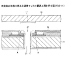
次いで、図10に示すように、金属膜34上に開口部36を有したレジスト膜35を形成する。開口部36は、金属膜34を露出するように、開口部32に設けられたレジスト膜35に形成されている。また、開口部36は、貫通孔21の形成位置に対応している。開口部36の直径R3は、開口部32の直径R2よりも小さくなるように設定されている(R3<R2)。
Next, as shown in FIG. 10, a resist
次いで、図11に示すように、レジスト膜35をマスクとして、金属膜34、電極パッド13、絶縁膜12を順次エッチングして、半導体基板11の第1の主面11Aを露出する。
Next, as illustrated in FIG. 11, the
具体的には、例えば、金属膜34としてTi/Cu積層膜を用いた場合、ウエットエッチング法により開口部36に露出されたCu膜を除去し、続いて、レジスト膜35をマスクとするドライエッチング法により、Ti膜、Al膜(電極パッド13に相当する)、SiO2膜(絶縁膜12に相当する)を順次エッチングする。
Specifically, for example, when a Ti / Cu laminated film is used as the
次いで、図12に示すように、第2の主面11B側から半導体基板11を薄板化する(基板薄板化工程)。半導体基板11の薄板化には、例えば、研削法やエッチング法を用いることができる。具体的には、例えば、グラインダーにより半導体基板の厚さM1が200μmになるまで薄板化する。
Next, as shown in FIG. 12, the
このように、貫通孔21を形成する前に半導体基板11を薄板化することで、貫通孔21のアスペクト比が小さくなるため、貫通孔21を容易に形成することができる。
Thus, by thinning the
次いで、図13に示すように、レジスト膜35をマスクとするドライエッチング法により、半導体基板11が貫通するまでエッチングを行って、貫通孔21を形成する(貫通孔形成工程)。貫通孔21の直径R4は、開口部32の直径R2よりも小さくなるように設定されている(R4<R2)。
Next, as shown in FIG. 13, etching is performed by a dry etching method using the resist
次いで、図14に示すように、レジスト膜35を除去する。レジスト膜35は、例えば、O2アッシングにより除去することができる。また、開口部32の直径R2と貫通孔21の直径R4との大きさが異なるため、貫通孔21と金属膜34が設けられた開口部32との間には、段差部分Aが形成される。
Next, as shown in FIG. 14, the resist
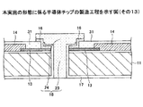
次いで、図15に示すように、図14に示した構造体の金属膜34上に、開口部32の上端部を覆うように絶縁膜除去用テープ38を貼り付ける(絶縁膜除去用テープ貼付工程)。絶縁膜除去用テープ38としては、例えば、PET基材にアクリル系粘着材を形成したものを用いることができる。絶縁膜除去用テープ38の厚さM5は、例えば、100μm〜200μmとすることができる。
Next, as shown in FIG. 15, the insulating
次いで、図16に示すように、半導体基板11の第2の主面11B側から貫通孔21の側壁に絶縁膜17を形成する(絶縁膜形成工程)。このとき、半導体基板11の第2の主面11B上、開口部32の側壁、及び絶縁膜除去用テープ38にも絶縁膜17が形成される。具体的には、CVD法により、貫通孔21の側壁及び半導体基板11の第2の主面11Bに、厚さが1μmとなるようSiO2膜を形成する。
Next, as shown in FIG. 16, the insulating
このように、半導体基板11の第2の主面11B側から、貫通孔21の側壁に絶縁膜17を形成することで、金属膜34が設けられた開口部32に形成される絶縁膜12の厚さを貫通孔21の側壁に形成される絶縁膜17の厚さM2よりも薄くして、段差部分Aに形成された絶縁膜17の強度を弱くすることができる。
Thus, by forming the insulating
次いで、図17に示すように、絶縁膜17が形成された絶縁膜除去用テープ38を金属膜34から取り除く(絶縁膜除去用テープ除去工程)。この際、絶縁膜17は、厚さが薄く、強度の弱い段差部分Aで破断し、不要な絶縁膜17(絶縁膜除去用テープ38上に形成された絶縁膜17)が絶縁膜除去用テープ38と共に除去される。
Next, as shown in FIG. 17, the insulating
このように、金属膜34上に開口部32を覆う絶縁膜除去用テープ38を貼り付け、半導体基板11の第2の主面11B側から、貫通孔21の側壁を覆うように絶縁膜17を形成することで、段差部分Aの絶縁膜17の厚さを貫通孔21の側壁に形成される絶縁膜17よりも薄くすることが可能となる。これにより、絶縁膜除去用テープ38を除去する際、絶縁膜17を段差部分Aで破断させて、貫通孔21の側壁を絶縁膜17で精度良く覆うことが可能となるため、半導体チップ10の歩留まりを向上させることができる。
As described above, the insulating
なお、開口部32の側壁に貫通孔21の側壁と同じだけの厚さの絶縁膜17が形成された場合でも、段差部分Aの角部に形成された絶縁膜17は貫通孔21の側壁に形成された絶縁膜17よりも強度が弱くなるため、絶縁膜除去用テープ38を除去する際、絶縁膜17は段差部分Aで破断する。
Even when the insulating
次いで、図18に示すように、絶縁膜17が形成された貫通孔21に貫通部23と、絶縁膜17及び金属膜34が形成された開口部32に開口部32から突出する突出部24とを形成する(貫通ビア形成工程)。これにより、貫通部23と突出部24とからなる貫通ビア18が形成される。
Next, as shown in FIG. 18, the through
具体的には、例えば、突出部24の形状に対応するようにパターニングしたレジスト膜を金属膜34上に形成し、その後、半導体基板11の第2の主面11B側に形成された絶縁膜17に金属板(例えば、Cu板)を配置し、この金属板を給電層として、電解めっき法により導電金属(例えば、Cu)を貫通孔21及び開口部32に析出させて、貫通ビア18を形成する。
Specifically, for example, a resist film patterned so as to correspond to the shape of the protruding
開口部32から突出した突出部24部分は、開口部32よりも幅広形状とされており、その直径R5は、例えば、90μmとすることができる。また、開口部32から突出した突出部24部分の厚さM6は、例えば、5μmとすることができる。
The protruding
なお、金属膜34を給電層として、電解めっき法により導電金属(例えば、Cu)を貫通孔21及び開口部32に析出させて、貫通ビア18を形成してもよい。
The through via 18 may be formed by using the
次いで、図19に示すように、エッチング法により突出部24に覆われていない金属膜34を除去して、突出部24と電極パッド13とに接触する導電部材16を形成する(導電部材形成工程)。
Next, as shown in FIG. 19, the
このように、開口部32から突出するように突出部24を形成すると共に、突出部24と電極パッド13とに接触する導電部材16を形成することにより、導電部材16を介して、貫通ビア18と電極パッド13とを電気的に接続することができる。
In this way, the projecting
次いで、図20に示すように、レジスト膜31を除去する。レジスト膜31は、例えば、O2アッシングにより除去する。これにより、半導体チップ10が製造される。
Next, as shown in FIG. 20, the resist
本実施の形態の半導体チップの製造方法によれば、金属膜34上に開口部32を覆う絶縁膜除去用テープ38を貼り付け、開口部32よりも直径の小さい貫通孔21の側壁を覆うように絶縁膜17を形成することで、貫通孔21と開口部32とから構成される段差部分Aの絶縁膜17の厚さが薄くなるため、絶縁膜除去用テープ38を除去する際、絶縁膜17が段差部分Aで破断する。これにより、貫通孔21の側壁を絶縁膜17により精度良く覆うことが可能となり、半導体チップ10の歩留まりを向上させることができる。
According to the semiconductor chip manufacturing method of the present embodiment, the insulating
以上、本発明の好ましい実施の形態について詳述したが、本発明はかかる特定の実施の形態に限定されるものではなく、特許請求の範囲内に記載された本発明の要旨の範囲内において、種々の変形・変更が可能である。 The preferred embodiments of the present invention have been described in detail above, but the present invention is not limited to such specific embodiments, and within the scope of the present invention described in the claims, Various modifications and changes are possible.
本発明は、歩留まりを向上させることのできる半導体チップの製造方法に適用できる。 The present invention can be applied to a method of manufacturing a semiconductor chip that can improve the yield.
10 半導体チップ
11 半導体基板
11A 第1の主面
11B 第2の主面
12,17 絶縁膜
13 電極パッド
13A 上面
14 保護膜
14A,32,36 開口部
16 導電部材
18 貫通ビア
21 貫通孔
23 貫通部
23A 下端部
24A 下面
24 突出部
31,35 レジスト膜
34 金属膜
38 絶縁膜除去用テープ
A 段差部分
D1 深さ
M1〜M6 厚さ
R1〜R5 直径
DESCRIPTION OF
Claims (3)
前記電極パッド上に第1開口部を有した第1のレジスト膜を形成する第1レジスト膜形成工程と、
前記第1開口部及び前記第1のレジスト膜を覆うように金属膜を形成する金属膜形成工程と、
前記第1開口部の形成位置に、前記第1開口部よりも直径の小さい第2開口部を有する第2のレジスト膜を、前記金属膜を覆うように形成する第2レジスト膜形成工程と、
前記金属膜、前記半導体基板及び電極パッドを貫通し、前記第2開口部の形成位置に対応する貫通孔を形成する貫通孔形成工程と、
前記第1開口部の上端部を覆うように絶縁膜除去用テープを設ける絶縁膜除去用テープ貼付工程と、
前記絶縁膜除去用テープ貼付工程後に、前記半導体基板の前記半導体素子の面と反対側の面側から、前記貫通孔の側壁及び前記第1開口部に前記絶縁膜を形成する絶縁膜形成工程と、
前記絶縁膜形成工程の後に前記絶縁膜除去用テープを除去する絶縁膜除去用テープ除去工程と、
前記絶縁膜除去用テープ除去工程の後に、前記貫通孔及び前記第1開口部に前記貫通ビアを形成する貫通ビア形成工程とを含むことを特徴とする半導体チップの製造方法。 A method of manufacturing a semiconductor chip, comprising: an electrode pad electrically connected to a semiconductor element formed on a semiconductor substrate; and a through via electrically connected to the electrode pad,
A first resist film forming step of forming a first resist film having a first opening on the electrode pads,
A metal film forming step of forming a metal film so as to cover the first opening and the first resist film;
A second resist film forming step of forming a second resist film having a second opening having a diameter smaller than that of the first opening so as to cover the metal film at a position where the first opening is formed;
A through hole forming step of penetrating the metal film, the semiconductor substrate and the electrode pad, and forming a through hole corresponding to the formation position of the second opening ;
An insulating film removing tape applying step of providing an insulating film removing tape so as to cover the upper end of the first opening ;
An insulating film forming step of forming the insulating film on the side wall of the through-hole and the first opening from the surface side of the semiconductor substrate opposite to the surface of the semiconductor element after the step of applying the insulating film removing tape; ,
An insulating film removing tape removing step of removing the insulating film removing tape after the insulating film forming step ;
A method of manufacturing a semiconductor chip, comprising: a through via forming step of forming the through via in the through hole and the first opening after the insulating film removing tape removing step .
前記貫通ビア形成工程の後に、前記金属膜のうち、前記突出部に覆われた部分以外を除去して、前記突出部と電極パッドとに接触する導電部材を形成する導電部材形成工程とをさらに設けたことを特徴とする請求項1記載の半導体チップの製造方法。 In the through via forming step, the protruding from the first opening to form the through via having the projecting portion which becomes wider shape than the first opening,
After the through via forming step, a conductive member forming step of removing a portion of the metal film other than the portion covered with the protruding portion to form a conductive member that contacts the protruding portion and the electrode pad, The semiconductor chip manufacturing method according to claim 1, wherein the semiconductor chip manufacturing method is provided.
Priority Applications (5)
| Application Number | Priority Date | Filing Date | Title |
|---|---|---|---|
| JP2005274242A JP4536629B2 (en) | 2005-09-21 | 2005-09-21 | Manufacturing method of semiconductor chip |
| US11/523,576 US7557037B2 (en) | 2005-09-21 | 2006-09-20 | Method of manufacturing semiconductor chip |
| KR1020060091081A KR20070033268A (en) | 2005-09-21 | 2006-09-20 | Manufacturing method of semiconductor chip |
| EP06019780.3A EP1768177B1 (en) | 2005-09-21 | 2006-09-21 | Method of manufacturing semiconductor chip |
| TW095134901A TW200717767A (en) | 2005-09-21 | 2006-09-21 | Method of manufacturing semiconductor chip |
Applications Claiming Priority (1)
| Application Number | Priority Date | Filing Date | Title |
|---|---|---|---|
| JP2005274242A JP4536629B2 (en) | 2005-09-21 | 2005-09-21 | Manufacturing method of semiconductor chip |
Publications (2)
| Publication Number | Publication Date |
|---|---|
| JP2007088163A JP2007088163A (en) | 2007-04-05 |
| JP4536629B2 true JP4536629B2 (en) | 2010-09-01 |
Family
ID=37561746
Family Applications (1)
| Application Number | Title | Priority Date | Filing Date |
|---|---|---|---|
| JP2005274242A Active JP4536629B2 (en) | 2005-09-21 | 2005-09-21 | Manufacturing method of semiconductor chip |
Country Status (5)
| Country | Link |
|---|---|
| US (1) | US7557037B2 (en) |
| EP (1) | EP1768177B1 (en) |
| JP (1) | JP4536629B2 (en) |
| KR (1) | KR20070033268A (en) |
| TW (1) | TW200717767A (en) |
Families Citing this family (4)
| Publication number | Priority date | Publication date | Assignee | Title |
|---|---|---|---|---|
| JP2011009645A (en) | 2009-06-29 | 2011-01-13 | Toshiba Corp | Semiconductor device and method of manufacturing the same |
| US9412806B2 (en) | 2014-06-13 | 2016-08-09 | Invensas Corporation | Making multilayer 3D capacitors using arrays of upstanding rods or ridges |
| US9397038B1 (en) | 2015-02-27 | 2016-07-19 | Invensas Corporation | Microelectronic components with features wrapping around protrusions of conductive vias protruding from through-holes passing through substrates |
| US9837375B2 (en) | 2016-02-26 | 2017-12-05 | Semtech Corporation | Semiconductor device and method of forming insulating layers around semiconductor die |
Citations (3)
| Publication number | Priority date | Publication date | Assignee | Title |
|---|---|---|---|---|
| JP2004207318A (en) * | 2002-12-24 | 2004-07-22 | Seiko Epson Corp | Semiconductor device, manufacturing method thereof circuit board, and electronic equipment |
| JP2004327910A (en) * | 2003-04-28 | 2004-11-18 | Sharp Corp | Semiconductor device and its manufacturing method |
| JP2005051142A (en) * | 2003-07-31 | 2005-02-24 | Nec Kansai Ltd | Method for manufacturing semiconductor device |
Family Cites Families (4)
| Publication number | Priority date | Publication date | Assignee | Title |
|---|---|---|---|---|
| JP3726579B2 (en) | 1999-08-20 | 2005-12-14 | セイコーエプソン株式会社 | Semiconductor device and manufacturing method thereof |
| JP4053257B2 (en) * | 2001-06-14 | 2008-02-27 | 新光電気工業株式会社 | Manufacturing method of semiconductor device |
| JP4322508B2 (en) * | 2003-01-15 | 2009-09-02 | 新光電気工業株式会社 | Manufacturing method of semiconductor device |
| US7199050B2 (en) * | 2004-08-24 | 2007-04-03 | Micron Technology, Inc. | Pass through via technology for use during the manufacture of a semiconductor device |
-
2005
- 2005-09-21 JP JP2005274242A patent/JP4536629B2/en active Active
-
2006
- 2006-09-20 KR KR1020060091081A patent/KR20070033268A/en not_active Application Discontinuation
- 2006-09-20 US US11/523,576 patent/US7557037B2/en active Active
- 2006-09-21 EP EP06019780.3A patent/EP1768177B1/en active Active
- 2006-09-21 TW TW095134901A patent/TW200717767A/en unknown
Patent Citations (3)
| Publication number | Priority date | Publication date | Assignee | Title |
|---|---|---|---|---|
| JP2004207318A (en) * | 2002-12-24 | 2004-07-22 | Seiko Epson Corp | Semiconductor device, manufacturing method thereof circuit board, and electronic equipment |
| JP2004327910A (en) * | 2003-04-28 | 2004-11-18 | Sharp Corp | Semiconductor device and its manufacturing method |
| JP2005051142A (en) * | 2003-07-31 | 2005-02-24 | Nec Kansai Ltd | Method for manufacturing semiconductor device |
Also Published As
| Publication number | Publication date |
|---|---|
| JP2007088163A (en) | 2007-04-05 |
| EP1768177A2 (en) | 2007-03-28 |
| US7557037B2 (en) | 2009-07-07 |
| EP1768177B1 (en) | 2017-02-08 |
| TW200717767A (en) | 2007-05-01 |
| US20070065980A1 (en) | 2007-03-22 |
| EP1768177A3 (en) | 2011-06-22 |
| KR20070033268A (en) | 2007-03-26 |
Similar Documents
| Publication | Publication Date | Title |
|---|---|---|
| JP5222459B2 (en) | Semiconductor chip manufacturing method, multichip package | |
| JP4250154B2 (en) | Semiconductor chip and manufacturing method thereof | |
| KR100512817B1 (en) | Semiconductor device and its manufacturing method, circuit board and electronic apparatus | |
| JP3918935B2 (en) | Manufacturing method of semiconductor device | |
| KR100641696B1 (en) | Method of manufacturing semiconductor device | |
| US7029937B2 (en) | Semiconductor device and method of manufacturing the same, circuit board, and electronic instrument | |
| US6642615B2 (en) | Semiconductor device and method of manufacturing the same, circuit board and electronic instrument | |
| KR101971279B1 (en) | Bump structure and the method for fabricating the same | |
| TWI591764B (en) | Chip package and manufacturing method thereof | |
| JP4536629B2 (en) | Manufacturing method of semiconductor chip | |
| US7135762B2 (en) | Semiconductor device, stacked semiconductor device, methods of manufacturing them, circuit board, and electronic instrument | |
| JP2019140145A (en) | Semiconductor device and manufacturing method thereof | |
| JP2006287094A (en) | Semiconductor apparatus and manufacturing method therefor | |
| US10651374B2 (en) | Semiconductor device, and method for manufacturing the same | |
| JP2009049134A (en) | Method of manufacturing semiconductor device | |
| JP2004221351A (en) | Semiconductor device and its manufacturing method, circuit board, and electronic apparatus | |
| JP2004221350A (en) | Semiconductor chip, semiconductor wafer, semiconductor device and its manufacturing method, circuit board, and electronic apparatus | |
| JP2005302816A (en) | Semiconductor device and its manufacturing method |
Legal Events
| Date | Code | Title | Description |
|---|---|---|---|
| A621 | Written request for application examination |
Free format text: JAPANESE INTERMEDIATE CODE: A621 Effective date: 20080410 |
|
| A977 | Report on retrieval |
Free format text: JAPANESE INTERMEDIATE CODE: A971007 Effective date: 20100408 |
|
| A131 | Notification of reasons for refusal |
Free format text: JAPANESE INTERMEDIATE CODE: A131 Effective date: 20100420 |
|
| A521 | Written amendment |
Free format text: JAPANESE INTERMEDIATE CODE: A523 Effective date: 20100524 |
|
| TRDD | Decision of grant or rejection written | ||
| A01 | Written decision to grant a patent or to grant a registration (utility model) |
Free format text: JAPANESE INTERMEDIATE CODE: A01 Effective date: 20100615 |
|
| A01 | Written decision to grant a patent or to grant a registration (utility model) |
Free format text: JAPANESE INTERMEDIATE CODE: A01 |
|
| A61 | First payment of annual fees (during grant procedure) |
Free format text: JAPANESE INTERMEDIATE CODE: A61 Effective date: 20100616 |
|
| FPAY | Renewal fee payment (event date is renewal date of database) |
Free format text: PAYMENT UNTIL: 20130625 Year of fee payment: 3 |
|
| R150 | Certificate of patent or registration of utility model |
Ref document number: 4536629 Country of ref document: JP Free format text: JAPANESE INTERMEDIATE CODE: R150 Free format text: JAPANESE INTERMEDIATE CODE: R150 |