EP1388909B1 - Converter for receiving satellite broadcast - Google Patents
Converter for receiving satellite broadcast Download PDFInfo
- Publication number
- EP1388909B1 EP1388909B1 EP20030254616 EP03254616A EP1388909B1 EP 1388909 B1 EP1388909 B1 EP 1388909B1 EP 20030254616 EP20030254616 EP 20030254616 EP 03254616 A EP03254616 A EP 03254616A EP 1388909 B1 EP1388909 B1 EP 1388909B1
- Authority
- EP
- European Patent Office
- Prior art keywords
- waveguide
- circuit substrate
- probe
- short
- linearly polarized
- Prior art date
- Legal status (The legal status is an assumption and is not a legal conclusion. Google has not performed a legal analysis and makes no representation as to the accuracy of the status listed.)
- Expired - Fee Related
Links
Images


Classifications
-
- H—ELECTRICITY
- H01—ELECTRIC ELEMENTS
- H01P—WAVEGUIDES; RESONATORS, LINES, OR OTHER DEVICES OF THE WAVEGUIDE TYPE
- H01P5/00—Coupling devices of the waveguide type
- H01P5/08—Coupling devices of the waveguide type for linking dissimilar lines or devices
- H01P5/10—Coupling devices of the waveguide type for linking dissimilar lines or devices for coupling balanced with unbalanced lines or devices
- H01P5/107—Hollow-waveguide/strip-line transitions
-
- H—ELECTRICITY
- H01—ELECTRIC ELEMENTS
- H01P—WAVEGUIDES; RESONATORS, LINES, OR OTHER DEVICES OF THE WAVEGUIDE TYPE
- H01P1/00—Auxiliary devices
- H01P1/16—Auxiliary devices for mode selection, e.g. mode suppression or mode promotion; for mode conversion
- H01P1/161—Auxiliary devices for mode selection, e.g. mode suppression or mode promotion; for mode conversion sustaining two independent orthogonal modes, e.g. orthomode transducer
Definitions
- the present invention relates to a converter for receiving a satellite broadcast which receives signals of two kinds of linearly polarized waves perpendicular to each other, and particularly relates to the converter for receiving the satellite broadcast in which a probe for detecting one of the linearly polarized waves is patterned and formed in a circuit substrate.
- Fig. 9 is a sectional view showing a conventional example of this kind of the converter for receiving the satellite broadcast.
- this converter for receiving the satellite broadcast has a waveguide 100 constructed by a metallic material of good electrical conductivity such as an aluminum die cast, a circuit substrate 101 forming a converter circuit, etc. therein, a cover body 102 formed in a shape having a bottom, etc.
- An unillustrated horn portion is integrally formed on one end side of the waveguide 100, and an opening portion 100a is formed by opening the other end side downward in Fig. 9 .
- An inclination face 100b opposed to the opening portion 100a is formed within the waveguide 100. This inclination face 100b crosses the tube axis of the waveguide 100 at an angle of about 45 degrees.
- an impedance converting portion 100c is formed within the waveguide 100. This impedance converting portion 100c is formed in a stepwise shape so as to gradually reduce an opening area toward the inclination face 100b.
- the circuit substrate 101 is overlapped with the outer wall face of the waveguide 100, and a notch hole 101a opposed to the opening portion 100a of the waveguide 100 is formed in this circuit substrate 101.
- a projecting piece 101b extended toward the center of the notch hole 101a is formed.
- the cover body 102 covers the notch hole 101a of the circuit substrate 101 and the projecting piece 101b, and is fixed to the waveguide 100 by using
- a first probe 104 constructed by a pin member and a first short-circuited terminal 105 are inserted into the waveguide 100.
- This first probe 104 is soldered to an input section of the above converter circuit formed in the circuit substrate 101.
- the first short-circuited terminal 105 is arranged to reflect a first linearly polarized wave (e.g., a vertically polarized wave) advanced into the waveguide 100, and detect the first linearly polarized wave by the first probe 104.
- This first short-circuited terminal 105 is set in the position separated by about 1/4 wavelength in the advancing direction of a radio wave from the first probe 104.
- a second probe 106 is patterned and formed in the projecting piece 101b of the circuit substrate.
- This second probe 106 is connected to the input section of the above converter circuit.
- the inner bottom face of the above cover body 102 is set to a second short-circuited terminal 107 for reflecting a second linearly polarized wave (e.g., a horizontally polarized wave) advanced into the waveguide 100 and detecting this second linearly polarized wave by the second probe 106.
- This second short-circuited terminal 107 is set in the position separated by about 1/4 wavelength in the advancing direction of the radio wave from the second probe 106.
- the converter for receiving the satellite broadcast constructed in this way, when the radio wave transmitted from a satellite enters from the above horn portion and is advanced into the waveguide 100 as the first and second linearly polarized waves perpendicular to each other, the first linearly polarized wave is reflected in the first short-circuited terminal 105 and is detected by the first probe 104. Further, the second linearly polarized wave passes through the impedance converting portion 100c and is directionally converted on the inclination face 100b. Thereafter, the second linearly polarized wave is reflected in the second short-circuited terminal 107 of the cover body 102, and is detected by the second probe 106.
- the two orthogonal polarized wave signals detected by these first and second probes 104, 106 are frequency-converted to IF frequency signals by the above converter circuit formed in the circuit substrate 101, and are then outputted through an unillustrated output terminal.
- the stepwise impedance converting portion 100c for passing only the second linearly polarized wave is formed within the waveguide 100. Therefore, matching with the second probe 106 can be taken even when the electric field of the second linearly polarized wave is slightly disturbed by the influences of the first short-circuited terminal 105 and the inclination face 100b. Further, electricity supply efficiency of the second probe 106 can be raised by the impedance converting portion 100c.
- an impedance converting portion 100c must be formed within the waveguide 100, a problem exists in that the waveguide 100 is lengthened in the tube axis direction and is not easily made compact. Further, a problem exists in that the entire shape of the waveguide 100 becomes complicated and manufacture cost is raised.
- a further prior art converter for receiving a satellite broadcast is known from EP 0788183 , which discloses providing an iris as part of a rectangular waveguide.
- the present invention is made in consideration of such a real situation of the prior art, and an object of the present invention is to provide a converter for receiving a satellite broadcast suitable for compactness and a reduction in cast.
- the present invention resides in a converter for receiving a satellite broadcast comprising a waveguide for advancing mutually perpendicular first and second linearly polarized radio waves, a first probe arranged so as to be projected into the waveguide, a first short-circuited terminal for reflecting said first linearly polarized wave and detecting this first linearly polarized wave by said first probe, a circuit substrate arranged at a rear portion opening end of said waveguide, a second probe patterned and formed in said circuit substrate and projecting into said waveguide, and a second short-circuited terminal for reflecting said second linearly polarized wave and detecting this second linearly polarized wave by said second probe; wherein said circuit substrate includes a substantially rectangular notch hole having long and short sides, the notch hole being defined by a ground conductor that is provided with a matching pattern that is projected into the waveguide and a cover body, and the second probe is projected toward the centre of the notch hole in a direction substantially orthogonal to the long sides of the notch hole
- the ground conductor faced and projected into the tube of the waveguide becomes a capacity component, and electricity supply efficiency of the second probe can be raised by patterning and adjusting this ground conductor as a matching pattern. Therefore, it is not necessary to arrange an impedance converting portion of a complicated shape within the waveguide so that the waveguide can be correspondingly formed in a simple shape, and can be shortened in the tube axis direction.
- the above circuit substrate can be arranged so as to be perpendicular to the tube axis of the waveguide.
- the circuit substrate in parallel with the tube axis of the waveguide, and arrange an inclination face for guiding the second linearly polarized wave to the second short-circuited terminal within the waveguide.
- the first short-circuited terminal can be also used as a fixing means of the cover body.
- the cover body it is preferable to integrally form the first short-circuited terminal in the cover body and extend this first short-circuited terminal through the circuit substrate and the tube interior of the waveguide and solder the first short-circuited terminal to the outer wall face of the waveguide since an assembly work can be simplified.
- Fig. 1 is a plan view of a converter for receiving a satellite broadcast in accordance with a first embodiment mode example.
- Fig. 2 is a sectional view along line II-II of Fig. 1 .
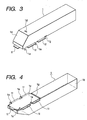
- Fig. 3 is a perspective view of a waveguide arranged in the converter for receiving the satellite broadcast.
- Fig. 4 is a perspective view of the waveguide seen from the side opposed to Fig. 3 .
- Fig. 5 is a plan view of a circuit substrate arranged in the converter for receiving the satellite broadcast.
- Fig. 6 is a rear view of the circuit substrate.
- Fig. 7 is a perspective view of a cover body arranged in the converter for receiving the satellite broadcast.
- the converter for receiving the satellite broadcast in accordance with this embodiment mode example has a waveguide 1 having an inclination face 1a on one end side thereof and formed in a square sleeve shape, and a circuit substrate 2 forming a converter circuit, etc. therein, a cover body 3 formed in a shape having a bottom, etc.
- the waveguide 1 is constructed by bending and processing a metallic plate, and an end face on the side opposed to the inclination face 1a of this waveguide 1 is set to a front portion opening end 1b of a square shape.
- An unillustrated dielectric feeder is attached to this front portion opening end 1b.
- a radio wave transmitted from a satellite is guided from this dielectric feeder into the waveguide 1, and is then advanced toward the inclination face 1a as first and second linearly polarized waves perpendicular to each other. If a 90-degree phase changing portion is arranged in this dielectric feeder, a circularly polarized wave transmitted from the satellite is converted to a linearly polarized wave, and can be guided into the waveguide 1. As shown in Figs.
- a rectangular opening 1c is formed on one side face of the waveguide 1, and a hole 1d is formed on the other side face of the waveguide 1 opposed to this opening 1c.
- Plural leg pieces 1e, plural bending pieces 1f and one engaging piece 1g are formed on the periphery of the opening 1c. Each bending piece 1f is bent from the opening 1c toward the outside, but the engaging piece 1g is bent inside toward the opening 1c.
- the inclination face 1a crosses the tube axis of the waveguide 1 at an angle of about 45 degrees.
- the radio wave entering from the side of the front portion opening end 1b of the waveguide 1 is perpendicularly returned on the inclination face 1a, and is advanced in the direction of the opening 1c.
- a rectangular notch hole 2a, plural engaging holes 2b and positioning holes 2c, one through hole 2d and a look-through hole 2e are respectively formed in the circuit substrate 2.
- a projecting piece 2f extended toward the center of the notch hole 2a is formed on a long side of the notch hole 2a.
- An inside ground conductor 4 and an outside ground conductor 5 are patterned and formed on the surface of this circuit substrate 2.
- a portion extended along the opposed long side of the notch hole 2a in the inside ground conductor 4 functions as a matching pattern 4a described later.
- a circuit element of an unillustrated converter circuit is mounted to the rear face of the circuit substrate 2.
- a second probe 6 connected to an input section of this converter circuit is patterned and formed on the projecting piece 2f.
- An outside ground conductor 7 is patterned and formed on the rear face of the circuit substrate 2 along its outer periphery.
- An inside ground conductor 8 is patterned and formed so as to surround the notch hole 2a. In this inside ground conductor 8, a portion extended along the opposed long side of the notch hole 2a functions as a matching pattern 8a described later.
- the matching patterns 4a, 8a on both the front and rear faces of the circuit substrate 2 are electrically conducted through many through holes 9.
- the cover body 3 is constructed by bending and processing a metallic plate in a square sleeve shape.
- Plural positioning projections 3a are integrally formed on an opposed side face of this cover body 3.
- a first short-circuited terminal 10 projected in a band shape is integrally formed on one side face of the cover body 3.
- the inner bottom face of the cover body 3 is set to a second short-circuited terminal 11.
- the engaging piece 1g of the waveguide 1 is engaged with one side face of the circuit substrate 2, and each bending piece 1f is soldered to the outside ground conductor 5 in a state in which each leg piece 1e is inserted into the corresponding engaging hole 2b.
- the waveguide 1 is placed and fixed onto the circuit substrate 2 such that its opening 1c is overlapped with the inside ground conductor 4.
- the opening 1c of the waveguide 1 is covered with the circuit substrate 2 in a portion except for the notch hole 2a.
- a rear portion opening end of the waveguide 1 is formed by the opening 1c overlapped with this notch hole 2a.
- a first probe 12 constructed by a pin member is inserted into the look-through hole 2e from the rear face side of the circuit substrate 2, and is then inserted into the waveguide 1. This first probe 12 is soldered to the input section of the above converter circuit formed in the circuit substrate 2.
- each positioning projection 3a of the cover body 3 is inserted into the corresponding positioning hole 2c of the circuit substrate 2.
- the first short-circuited terminal 10 is inserted into the hole 1d from the through hole 2d and is soldered to the outside face of the waveguide 1 so that the cover body 3 is f ixed to the rear face side of the circuit substrate 2.
- a rear portion opening end of the waveguide 1 and the notch hole 2a of the circuit substrate 2 are covered with the cover body 3.
- the first short-circuited terminal 10 is arranged within the waveguide 1 in the position separated by about 1/4 wavelength in the advancing direction of the radio wave from the first probe 12.
- the second short-circuited terminal 11 is arranged in the position separated by about 1/4 wavelength in the advancing direction of the radio wave from the second probe 6.
- This first short-circuited terminal 10 is arranged to reflect a first linearly polarized wave (e.g., a vertically polarized wave) advanced within the waveguide 1 and detect this first linearly polarized wave by the first probe 12.
- the second short-circuited terminal 11 is arranged to reflect a second linearly polarized wave (e.g., a horizontally polarized wave) and detect this second linearly polarized wave by the second probe 6.
- a frame body 13 constructed by a metallic material is fixed to the rear face side of the circuit substrate 2. This frame body 13 is soldered to the outs ide ground conductor 7 on the rear face of the circuit substrate 2.
- the above converter circuit formed on the rear face of the circuit substrate 2 is electrically shielded by covering an opening of this frame body 13 with a cover 14.
- the radio wave transmitted from the satellite enters the interior of the waveguide 1 from an unillustrated feeder attached to the front portion opening end 1b.
- this radio wave is advanced into the waveguide 1 as the first and second linearly polarized waves perpendicular to each other, the first linearly polarized wave is reflected in the first short-circuited terminal 10, and is detected by the first probe 12.
- the second linearly polarized wave is directionally converted on the inclination face 1a of the waveguide 1, and is then reflected in the second short-circuited terminal 11 of the cover body 3, and is detected by the second probe 6 on the circuit substrate 2.
- matching patterns 4a, 8a are formed on both the front and rear faces of the circuit substrate 2 outside the notch hole 2a faced and projected to the interior of the cover body 3 and the waveguide 1. These matching patterns 4a, 8a are extended in the direction perpendicular to the projecting direction of the second probe 6. Therefore, a reactance component of the second probe 6 and capacity components of the matching patterns 4a, 8a are generated within the waveguide 1 and the cover body 3. Accordingly, matching with the second probe 6 can be taken by suitably setting a pattern shape including the widths and the lengths of the matching patterns 4a, 8a even when the electric field of the second linearly polarized wave is slightly disturbed by the influences of the first short-circuited terminal 10 and the inclination face 1a.
- the matching patterns 4a, 8a extended in the direction perpendicular to the projecting direction of the second probe 6 are formed outside the notch hole 2a of the circuit substrate 2, and are faced and projected into the waveguide 1 and the cover body 3. Accordingly, the electricity supply efficiency of the second probe 6 can be raised without arranging an impedance converting portion of a complicated shape within the waveguide 1. Accordingly, the waveguide 1 of a simple shape formed by bending and processing a metallic plate can be used so that manufacture cost of the waveguide 1 can be correspondingly reduced, and the size of the waveguide 1 can be shortened in the tube axis direction and the waveguide 1 can be made compact.
- the matching patterns 4a, 8a are formed on both the front and rear faces of the circuit substrate 2 and both the matching patterns 4a, 8a are conducted through a through hole 9, the degree of freedom of the pattern shapes of the matching patterns 4a, 8a is widened, and matching of the second linearly polarized wave and the second probe 6 can be simply taken.
- the first short-circuited terminal 10 is integrally formed in the cover body 3, and is extended through the circuit substrate 2 and the tube interior of the waveguide 1 and is soldered to the outer wall face of the waveguide 1. Accordingly, the first short-circuited terminal 10 can be also used as a fixing means of the cover body 3, and an assembly work can be simplified.
- Fig. 8 is a sectional view of a main portion of a converter for receiving the satellite broadcast in accordance with a second embodiment mode example.
- portions corresponding to those of Fig. 2 are designated by the same reference numerals. broadcast
- the converter for receiving the satellite broadcast in accordance with this embodiment mode example differs from that in the above first embodiment mode example in that each of a waveguide 20 and a cover body 21 is formed by a metallic material such as an aluminum die cast, and a first short-circuited terminal 22 is formed by a member separated from the cover body 21.
- the other constructions are fundamentally the same as the first embodiment mode example. Namely, the waveguide 20 has a front portion opening end 20a on one end side thereof, and a rear portion opening end 20b is formed on the other end side. An inclination face 20c opposed to the rear portion opening end 20b is formed within the waveguide 20.
- the circuit substrate 2 is constructed similarly to the first embodiment mode example, and the cover body 21 covers the rear portion opening end 20b of the waveguide 1 and the notch hole 2a of the circuit substrate 2, and is fixed to the waveguide 20 by using a first short-circuited terminal 22 and a screw 23.
- matching patterns 4a, 8a extended in the direction perpendicular to the projecting direction of the second probe 6 are formed outside the notch hole 2a of the circuit substrate 2.
- These matching patterns 4a, 8a are faced and projected into the waveguide 20 and the cover body 21. Accordingly, electricity supply efficiency of the second probe 6 can be raised without arranging an impedance converting portion of a complicated shape within the waveguide 20 so that the waveguide 20 can be correspondingly formed in a simple shape and its manufacture cost can be reduced. Further, the size of the waveguide 20 is shortened in the tube axis direction, and the waveguide 20 can be made compact.
- the waveguides 1, 20 having the inclination faces 1a, 20c therein are used, and the converter for receiving the satellite broadcast and having the circuit substrate 2 arranged in parallel with the tube axis of each of such waveguides 1, 20 has been explained.
- the waveguide of a straight shape having no inclination face therein can be also used, and the present invention can be also applied to the converter for receiving the satellite broadcast and having the circuit substrate arranged perpendicularly to the tube axis of such a waveguide.
- the explanation has been made with respect to the case in which the matching patterns 4a, 8a are formed on both the front and rear faces of the circuit substrate 2.
- one of the matching patterns 4a, 8a may be omitted.
- the present invention is embodied in the modes explained above, and has effects described below.
- the conver ter for receiving the satellite broadcast has a waveguide for advancing a radio wave entering a waveguide tube as first and second linearly polarized waves perpendicular to each other, a first probe arranged so as to be projected into the tube of this waveguide, a first short-circuited terminal for reflecting the first linearly polarized wave and detecting this first linearly polarized wave by the first probe, a circuit substrate arranged at a rear portion opening end of the waveguide, a second probe patterned and formed in this circuit substrate and projected into the tube of the waveguide, and a second short-circuited terminal for reflecting the second linearly polarized wave and detecting this second linearly polarized wave by the second probe; wherein a ground conductor extended in the direction approximately perpendicular to the projecting direction of the second probe is patterned and formed in the circuit substrate, and is faced and projected into the tube of the waveguide.
- the ground conductor faced and projected into the tube of the waveguide becomes a capacity component, and electricity supply efficiency of the second probe can be raised by patterning and adjusting this ground conductor as a matching pattern. Therefore, it is not necessary to arrange an impedance converting portion of a complicated shape within the waveguide, and the waveguide can be formed in a simple shape, and can be shortened in the tube axis direction.
Description
- The present invention relates to a converter for receiving a satellite broadcast which receives signals of two kinds of linearly polarized waves perpendicular to each other, and particularly relates to the converter for receiving the satellite broadcast in which a probe for detecting one of the linearly polarized waves is patterned and formed in a circuit substrate.
-
Fig. 9 is a sectional view showing a conventional example of this kind of the converter for receiving the satellite broadcast. As shown in this figure, this converter for receiving the satellite broadcast has awaveguide 100 constructed by a metallic material of good electrical conductivity such as an aluminum die cast, acircuit substrate 101 forming a converter circuit, etc. therein, acover body 102 formed in a shape having a bottom, etc. - An unillustrated horn portion is integrally formed on one end side of the
waveguide 100, and anopening portion 100a is formed by opening the other end side downward inFig. 9 . Aninclination face 100b opposed to theopening portion 100a is formed within thewaveguide 100. Thisinclination face 100b crosses the tube axis of thewaveguide 100 at an angle of about 45 degrees. Further, animpedance converting portion 100c is formed within thewaveguide 100. Thisimpedance converting portion 100c is formed in a stepwise shape so as to gradually reduce an opening area toward theinclination face 100b. Thecircuit substrate 101 is overlapped with the outer wall face of thewaveguide 100, and anotch hole 101a opposed to theopening portion 100a of thewaveguide 100 is formed in thiscircuit substrate 101. A projectingpiece 101b extended toward the center of thenotch hole 101a is formed. Thecover body 102 covers thenotch hole 101a of thecircuit substrate 101 and theprojecting piece 101b, and is fixed to thewaveguide 100 by usingplural screws 103. - A
first probe 104 constructed by a pin member and a first short-circuitedterminal 105 are inserted into thewaveguide 100. Thisfirst probe 104 is soldered to an input section of the above converter circuit formed in thecircuit substrate 101. The first short-circuited terminal 105 is arranged to reflect a first linearly polarized wave (e.g., a vertically polarized wave) advanced into thewaveguide 100, and detect the first linearly polarized wave by thefirst probe 104. This first short-circuited terminal 105 is set in the position separated by about 1/4 wavelength in the advancing direction of a radio wave from thefirst probe 104. In contrast to this, asecond probe 106 is patterned and formed in the projectingpiece 101b of the circuit substrate. Thissecond probe 106 is connected to the input section of the above converter circuit. The inner bottom face of theabove cover body 102 is set to a second short-circuited terminal 107 for reflecting a second linearly polarized wave (e.g., a horizontally polarized wave) advanced into thewaveguide 100 and detecting this second linearly polarized wave by thesecond probe 106. This second short-circuited terminal 107 is set in the position separated by about 1/4 wavelength in the advancing direction of the radio wave from thesecond probe 106. - In the converter for receiving the satellite broadcast constructed in this way, when the radio wave transmitted from a satellite enters from the above horn portion and is advanced into the
waveguide 100 as the first and second linearly polarized waves perpendicular to each other, the first linearly polarized wave is reflected in the first short-circuited terminal 105 and is detected by thefirst probe 104. Further, the second linearly polarized wave passes through theimpedance converting portion 100c and is directionally converted on theinclination face 100b. Thereafter, the second linearly polarized wave is reflected in the second short-circuited terminal 107 of thecover body 102, and is detected by thesecond probe 106. The two orthogonal polarized wave signals detected by these first andsecond probes circuit substrate 101, and are then outputted through an unillustrated output terminal. - In the above conventional converter for receiving the satellite broadcast, the stepwise
impedance converting portion 100c for passing only the second linearly polarized wave is formed within thewaveguide 100. Therefore, matching with thesecond probe 106 can be taken even when the electric field of the second linearly polarized wave is slightly disturbed by the influences of the first short-circuited terminal 105 and theinclination face 100b. Further, electricity supply efficiency of thesecond probe 106 can be raised by theimpedance converting portion 100c. However, since such animpedance converting portion 100c must be formed within thewaveguide 100, a problem exists in that thewaveguide 100 is lengthened in the tube axis direction and is not easily made compact. Further, a problem exists in that the entire shape of thewaveguide 100 becomes complicated and manufacture cost is raised. - A further prior art converter for receiving a satellite broadcast is known from
EP 0788183 , which discloses providing an iris as part of a rectangular waveguide. - The present invention is made in consideration of such a real situation of the prior art, and an object of the present invention is to provide a converter for receiving a satellite broadcast suitable for compactness and a reduction in cast.
- To achieve the above object, the present invention resides in a converter for receiving a satellite broadcast comprising a waveguide for advancing mutually perpendicular first and second linearly polarized radio waves, a first probe arranged so as to be projected into the waveguide, a first short-circuited terminal for reflecting said first linearly polarized wave and detecting this first linearly polarized wave by said first probe, a circuit substrate arranged at a rear portion opening end of said waveguide, a second probe patterned and formed in said circuit substrate and projecting into said waveguide, and a second short-circuited terminal for reflecting said second linearly polarized wave and detecting this second linearly polarized wave by said second probe; wherein said circuit substrate includes a substantially rectangular notch hole having long and short sides, the notch hole being defined by a ground conductor that is provided with a matching pattern that is projected into the waveguide and a cover body, and the second probe is projected toward the centre of the notch hole in a direction substantially orthogonal to the long sides of the notch hole, characterised in that the matching pattern is provided on at least one face of said circuit substrate.
- In the converter for receiving the satellite broadcast constructed in this way, the ground conductor faced and projected into the tube of the waveguide becomes a capacity component, and electricity supply efficiency of the second probe can be raised by patterning and adjusting this ground conductor as a matching pattern. Therefore, it is not necessary to arrange an impedance converting portion of a complicated shape within the waveguide so that the waveguide can be correspondingly formed in a simple shape, and can be shortened in the tube axis direction.
- In the above construction, it is sufficient to pattern and form the above ground conductor on at least one face of the circuit substrate. However, it is preferable to pattern and form the ground conductor on both the front and rear faces of the circuit substrate, and connect these ground conductors to each other through a through hole.
- Further, in the above construction, the above circuit substrate can be arranged so as to be perpendicular to the tube axis of the waveguide. However, it is preferable to arrange the circuit substrate in parallel with the tube axis of the waveguide, and arrange an inclination face for guiding the second linearly polarized wave to the second short-circuited terminal within the waveguide. In this case, when the second short-circuited terminal is arranged on the inner bottom face of a cover body and this cover body is arranged oppositely to a rear portion opening end of the waveguide through the circuit substrate and is fixed to the waveguide by the first short-circuited terminal, the first short-circuited terminal can be also used as a fixing means of the cover body. In this case, it is preferable to integrally form the first short-circuited terminal in the cover body and extend this first short-circuited terminal through the circuit substrate and the tube interior of the waveguide and solder the first short-circuited terminal to the outer wall face of the waveguide since an assembly work can be simplified.
- Embodiments of the invention will now be described, by way of example only, with reference to the accompanying drawings, in which:
-
Fig. 1 is a plan view of a converter for receiving a satellite broadcast in accordance with a first embodiment mode example of the present invention; -
Fig. 2 is a sectional view along line II-II ofFig. 1 ; -
Fig. 3 is a perspective view of a waveguide arranged in the converter for receiving the satellite broadcast; -
Fig. 4 is a perspective view of the waveguide seen from the side opposed toFig. 3 ; -
Fig. 5 is a plan view of a circuit substrate arranged in the converter for receiving the satellite broadcast; -
Fig. 6 is a rear view of the circuit substrate; -
Fig. 7 is a perspective view of a cover body arranged in the converter for receiving the satellite broadcast; -
Fig. 8 is a sectional view of a main portion of a converter for receiving the satellite broadcast in accordance with a second embodiment mode example of the present invention.; and -
Fig. 9 is a sectional view of a converter for receiving the satellite broadcast in a conventional example. - The embodiment modes of the invention will next be explained with reference to the drawings.
Fig. 1 is a plan view of a converter for receiving a satellite broadcast in accordance with a first embodiment mode example.Fig. 2 is a sectional view along line II-II ofFig. 1 .Fig. 3 is a perspective view of a waveguide arranged in the converter for receiving the satellite broadcast.Fig. 4 is a perspective view of the waveguide seen from the side opposed toFig. 3 .Fig. 5 is a plan view of a circuit substrate arranged in the converter for receiving the satellite broadcast.Fig. 6 is a rear view of the circuit substrate.Fig. 7 is a perspective view of a cover body arranged in the converter for receiving the satellite broadcast. - The converter for receiving the satellite broadcast in accordance with this embodiment mode example has a waveguide 1 having an
inclination face 1a on one end side thereof and formed in a square sleeve shape, and acircuit substrate 2 forming a converter circuit, etc. therein, acover body 3 formed in a shape having a bottom, etc. - The waveguide 1 is constructed by bending and processing a metallic plate, and an end face on the side opposed to the
inclination face 1a of this waveguide 1 is set to a frontportion opening end 1b of a square shape. An unillustrated dielectric feeder is attached to this frontportion opening end 1b. A radio wave transmitted from a satellite is guided from this dielectric feeder into the waveguide 1, and is then advanced toward theinclination face 1a as first and second linearly polarized waves perpendicular to each other. If a 90-degree phase changing portion is arranged in this dielectric feeder, a circularly polarized wave transmitted from the satellite is converted to a linearly polarized wave, and can be guided into the waveguide 1. As shown inFigs. 3 and 4 , arectangular opening 1c is formed on one side face of the waveguide 1, and ahole 1d is formed on the other side face of the waveguide 1 opposed to thisopening 1c.Plural leg pieces 1e,plural bending pieces 1f and oneengaging piece 1g are formed on the periphery of theopening 1c. Eachbending piece 1f is bent from theopening 1c toward the outside, but the engagingpiece 1g is bent inside toward theopening 1c. Theinclination face 1a crosses the tube axis of the waveguide 1 at an angle of about 45 degrees. The radio wave entering from the side of the frontportion opening end 1b of the waveguide 1 is perpendicularly returned on theinclination face 1a, and is advanced in the direction of theopening 1c. - As shown in
Figs. 5 and 6 , arectangular notch hole 2a, plural engagingholes 2b andpositioning holes 2c, one throughhole 2d and a look-throughhole 2e are respectively formed in thecircuit substrate 2. A projectingpiece 2f extended toward the center of thenotch hole 2a is formed on a long side of thenotch hole 2a. Aninside ground conductor 4 and an outside ground conductor 5 are patterned and formed on the surface of thiscircuit substrate 2. A portion extended along the opposed long side of thenotch hole 2a in theinside ground conductor 4 functions as amatching pattern 4a described later. In contrast to this, a circuit element of an unillustrated converter circuit is mounted to the rear face of thecircuit substrate 2. Asecond probe 6 connected to an input section of this converter circuit is patterned and formed on the projectingpiece 2f. Anoutside ground conductor 7 is patterned and formed on the rear face of thecircuit substrate 2 along its outer periphery. Aninside ground conductor 8 is patterned and formed so as to surround thenotch hole 2a. In thisinside ground conductor 8, a portion extended along the opposed long side of thenotch hole 2a functions as amatching pattern 8a described later. Thematching patterns circuit substrate 2 are electrically conducted through many throughholes 9. - As shown in
Fig. 7 , thecover body 3 is constructed by bending and processing a metallic plate in a square sleeve shape.Plural positioning projections 3a are integrally formed on an opposed side face of thiscover body 3. Further, a first short-circuitedterminal 10 projected in a band shape is integrally formed on one side face of thecover body 3. The inner bottom face of thecover body 3 is set to a second short-circuitedterminal 11. - As shown in
Figs. 1 and 2 , the engagingpiece 1g of the waveguide 1 is engaged with one side face of thecircuit substrate 2, and eachbending piece 1f is soldered to the outside ground conductor 5 in a state in which eachleg piece 1e is inserted into the corresponding engaginghole 2b. Thus, the waveguide 1 is placed and fixed onto thecircuit substrate 2 such that its opening 1c is overlapped with theinside ground conductor 4. Thus, theopening 1c of the waveguide 1 is covered with thecircuit substrate 2 in a portion except for thenotch hole 2a. A rear portion opening end of the waveguide 1 is formed by the opening 1c overlapped with thisnotch hole 2a. Afirst probe 12 constructed by a pin member is inserted into the look-throughhole 2e from the rear face side of thecircuit substrate 2, and is then inserted into the waveguide 1. Thisfirst probe 12 is soldered to the input section of the above converter circuit formed in thecircuit substrate 2. - Further, each
positioning projection 3a of thecover body 3 is inserted into thecorresponding positioning hole 2c of thecircuit substrate 2. The first short-circuitedterminal 10 is inserted into thehole 1d from the throughhole 2d and is soldered to the outside face of the waveguide 1 so that thecover body 3 is f ixed to the rear face side of thecircuit substrate 2. Thus, a rear portion opening end of the waveguide 1 and thenotch hole 2a of thecircuit substrate 2 are covered with thecover body 3. The first short-circuitedterminal 10 is arranged within the waveguide 1 in the position separated by about 1/4 wavelength in the advancing direction of the radio wave from thefirst probe 12. The second short-circuitedterminal 11 is arranged in the position separated by about 1/4 wavelength in the advancing direction of the radio wave from thesecond probe 6. This first short-circuitedterminal 10 is arranged to reflect a first linearly polarized wave (e.g., a vertically polarized wave) advanced within the waveguide 1 and detect this first linearly polarized wave by thefirst probe 12. The second short-circuitedterminal 11 is arranged to reflect a second linearly polarized wave (e.g., a horizontally polarized wave) and detect this second linearly polarized wave by thesecond probe 6. Further, aframe body 13 constructed by a metallic material is fixed to the rear face side of thecircuit substrate 2. Thisframe body 13 is soldered to the outside ground conductor 7 on the rear face of thecircuit substrate 2. The above converter circuit formed on the rear face of thecircuit substrate 2 is electrically shielded by covering an opening of thisframe body 13 with acover 14. - In the converter for receiving the satellite broadcast constructed in this way, the radio wave transmitted from the satellite enters the interior of the waveguide 1 from an unillustrated feeder attached to the front
portion opening end 1b. When this radio wave is advanced into the waveguide 1 as the first and second linearly polarized waves perpendicular to each other, the first linearly polarized wave is reflected in the first short-circuitedterminal 10, and is detected by thefirst probe 12. Further, the second linearly polarized wave is directionally converted on theinclination face 1a of the waveguide 1, and is then reflected in the second short-circuitedterminal 11 of thecover body 3, and is detected by thesecond probe 6 on thecircuit substrate 2. Here, matchingpatterns circuit substrate 2 outside thenotch hole 2a faced and projected to the interior of thecover body 3 and the waveguide 1. These matchingpatterns second probe 6. Therefore, a reactance component of thesecond probe 6 and capacity components of thematching patterns cover body 3. Accordingly, matching with thesecond probe 6 can be taken by suitably setting a pattern shape including the widths and the lengths of thematching patterns terminal 10 and theinclination face 1a. Accordingly, electricity supply efficiency of thesecond probe 6 can be raised. These two orthogonal polarized wave signals detected by the first andsecond probes circuit substrate 2, and are then outputted through an unillustrated output terminal. - In the above converter for receiving the satellite broadcast in accordance with the first embodiment mode example, the
matching patterns second probe 6 are formed outside thenotch hole 2a of thecircuit substrate 2, and are faced and projected into the waveguide 1 and thecover body 3. Accordingly, the electricity supply efficiency of thesecond probe 6 can be raised without arranging an impedance converting portion of a complicated shape within the waveguide 1. Accordingly, the waveguide 1 of a simple shape formed by bending and processing a metallic plate can be used so that manufacture cost of the waveguide 1 can be correspondingly reduced, and the size of the waveguide 1 can be shortened in the tube axis direction and the waveguide 1 can be made compact. Further, since thematching patterns circuit substrate 2 and both thematching patterns hole 9, the degree of freedom of the pattern shapes of thematching patterns second probe 6 can be simply taken. Further, the first short-circuitedterminal 10 is integrally formed in thecover body 3, and is extended through thecircuit substrate 2 and the tube interior of the waveguide 1 and is soldered to the outer wall face of the waveguide 1. Accordingly, the first short-circuitedterminal 10 can be also used as a fixing means of thecover body 3, and an assembly work can be simplified. -
Fig. 8 is a sectional view of a main portion of a converter for receiving the satellite broadcast in accordance with a second embodiment mode example. InFig. 8 , portions corresponding to those ofFig. 2 are designated by the same reference numerals. broadcast - The converter for receiving the satellite broadcast in accordance with this embodiment mode example differs from that in the above first embodiment mode example in that each of a
waveguide 20 and acover body 21 is formed by a metallic material such as an aluminum die cast, and a first short-circuitedterminal 22 is formed by a member separated from thecover body 21. The other constructions are fundamentally the same as the first embodiment mode example. Namely, thewaveguide 20 has a frontportion opening end 20a on one end side thereof, and a rearportion opening end 20b is formed on the other end side. An inclination face 20c opposed to the rearportion opening end 20b is formed within thewaveguide 20. Thecircuit substrate 2 is constructed similarly to the first embodiment mode example, and thecover body 21 covers the rearportion opening end 20b of the waveguide 1 and thenotch hole 2a of thecircuit substrate 2, and is fixed to thewaveguide 20 by using a first short-circuitedterminal 22 and a screw 23. - In the converter for receiving the satellite broadcast in accordance with the second embodiment mode example constructed in this way, matching
patterns second probe 6 are formed outside thenotch hole 2a of thecircuit substrate 2. These matchingpatterns waveguide 20 and thecover body 21. Accordingly, electricity supply efficiency of thesecond probe 6 can be raised without arranging an impedance converting portion of a complicated shape within thewaveguide 20 so that thewaveguide 20 can be correspondingly formed in a simple shape and its manufacture cost can be reduced. Further, the size of thewaveguide 20 is shortened in the tube axis direction, and thewaveguide 20 can be made compact. - Further, in the above first and second embodiment mode examples, the
waveguides 1, 20 having the inclination faces 1a, 20c therein are used, and the converter for receiving the satellite broadcast and having thecircuit substrate 2 arranged in parallel with the tube axis of each ofsuch waveguides 1, 20 has been explained. However, the waveguide of a straight shape having no inclination face therein can be also used, and the present invention can be also applied to the converter for receiving the satellite broadcast and having the circuit substrate arranged perpendicularly to the tube axis of such a waveguide. the a.bove first and second embodiment - Further, in the above first and second embodiment mode examples, the explanation has been made with respect to the case in which the
matching patterns circuit substrate 2. However, one of thematching patterns - The present invention is embodied in the modes explained above, and has effects described below.
- The conver ter for receiving the satellite broadcast has a waveguide for advancing a radio wave entering a waveguide tube as first and second linearly polarized waves perpendicular to each other, a first probe arranged so as to be projected into the tube of this waveguide, a first short-circuited terminal for reflecting the first linearly polarized wave and detecting this first linearly polarized wave by the first probe, a circuit substrate arranged at a rear portion opening end of the waveguide, a second probe patterned and formed in this circuit substrate and projected into the tube of the waveguide, and a second short-circuited terminal for reflecting the second linearly polarized wave and detecting this second linearly polarized wave by the second probe; wherein a ground conductor extended in the direction approximately perpendicular to the projecting direction of the second probe is patterned and formed in the circuit substrate, and is faced and projected into the tube of the waveguide. Accordingly, the ground conductor faced and projected into the tube of the waveguide becomes a capacity component, and electricity supply efficiency of the second probe can be raised by patterning and adjusting this ground conductor as a matching pattern. Therefore, it is not necessary to arrange an impedance converting portion of a complicated shape within the waveguide, and the waveguide can be formed in a simple shape, and can be shortened in the tube axis direction.
Claims (5)
- A converter for receiving a satellite broadcast comprising a waveguide (1) for advancing mutually perpendicular first and second linearly polarized radio waves, a first probe (12) arranged so as to be projected into the waveguide, a first short-circuited terminal (10) for reflecting said first linearly polarized wave and detecting this first linearly polarized wave by said first probe, a circuit substrate (2) arranged at a rear portion opening end (1c) of said waveguide, a second probe (6) patterned and formed in said circuit substrate and projecting into said waveguide, and a second short-circuited terminal (11) for reflecting said second linearly polarized wave and detecting this second linearly polarized wave by said second probe;
wherein said circuit substrate includes a substantially rectangular notch hole (2a) having long and short sides, the notch hole being defined by a ground conductor (4, 8) that is provided with a matching pattern (4a, 8a) that is extended in the direction approximately perpendicular to the projecting direction of said second probe (6) and projected into the waveguide (1) and a cover body (3), and the second probe is projected toward the centre of the notch hole in a direction substantially orthogonal to the long sides of the notch hole,
characterised in that the matching pattern is provided on at least one face of said circuit substrate (2). - The converter according to Claim 1, wherein said ground conductor is patterned and formed on both front and rear faces of said circuit substrate, and these conductor patterns are connected to each other through a through hole (9).
- The converter according to Claim 1 or 2, wherein said circuit substrate is arranged in parallel with a tube axis of said waveguide, and said waveguide includes an inclination face (1a) for guiding said second linearly polarized wave to said second short-circuited terminal.
- The converter according to Claim 3, wherein said second short-circuited terminal is arranged on the inner bottom face of the cover body (3), and the cover body is arranged oppositely to the rear portion opening end.of said waveguide through said circuit substrate, and is fixed to said waveguide by said first short-circuited terminal.
- The converter according to Claim 4, wherein said first short-circuited terminal is integrally formed with said cover body, and extends through said circuit substrate and the interior of said waveguide, and is soldered to the outer wall face of the waveguide.
Applications Claiming Priority (2)
| Application Number | Priority Date | Filing Date | Title |
|---|---|---|---|
| JP2002227396A JP3916530B2 (en) | 2002-08-05 | 2002-08-05 | Converter for satellite broadcasting reception |
| JP2002227396 | 2002-08-05 |
Publications (2)
| Publication Number | Publication Date |
|---|---|
| EP1388909A1 EP1388909A1 (en) | 2004-02-11 |
| EP1388909B1 true EP1388909B1 (en) | 2008-07-02 |
Family
ID=30437725
Family Applications (1)
| Application Number | Title | Priority Date | Filing Date |
|---|---|---|---|
| EP20030254616 Expired - Fee Related EP1388909B1 (en) | 2002-08-05 | 2003-07-24 | Converter for receiving satellite broadcast |
Country Status (4)
| Country | Link |
|---|---|
| EP (1) | EP1388909B1 (en) |
| JP (1) | JP3916530B2 (en) |
| CN (1) | CN1271798C (en) |
| DE (1) | DE60321867D1 (en) |
Families Citing this family (2)
| Publication number | Priority date | Publication date | Assignee | Title |
|---|---|---|---|---|
| US9019033B2 (en) | 2011-12-23 | 2015-04-28 | Tyco Electronics Corporation | Contactless connector |
| WO2014116420A1 (en) * | 2013-01-22 | 2014-07-31 | Tyco Electronics Corporation | Contactless connector |
Family Cites Families (4)
| Publication number | Priority date | Publication date | Assignee | Title |
|---|---|---|---|---|
| DE69308906T2 (en) * | 1992-01-21 | 1997-09-11 | Sharp Kk | Waveguide coaxial transition and converter for satellite broadcast antenna with such a waveguide |
| US5585768A (en) * | 1995-07-12 | 1996-12-17 | Microelectronics Technology Inc. | Electromagnetic wave conversion device for receiving first and second signal components |
| GB2334153B (en) * | 1995-07-19 | 1999-11-17 | Alps Electric Co Ltd | Outdoor converter for receiving satellite broadcast |
| JP3771094B2 (en) * | 1999-10-04 | 2006-04-26 | アルプス電気株式会社 | Converter for satellite broadcasting reception |
-
2002
- 2002-08-05 JP JP2002227396A patent/JP3916530B2/en not_active Expired - Fee Related
-
2003
- 2003-07-24 DE DE60321867T patent/DE60321867D1/en not_active Expired - Lifetime
- 2003-07-24 EP EP20030254616 patent/EP1388909B1/en not_active Expired - Fee Related
- 2003-08-05 CN CN 03152588 patent/CN1271798C/en not_active Expired - Fee Related
Also Published As
| Publication number | Publication date |
|---|---|
| EP1388909A1 (en) | 2004-02-11 |
| CN1271798C (en) | 2006-08-23 |
| CN1481091A (en) | 2004-03-10 |
| DE60321867D1 (en) | 2008-08-14 |
| JP3916530B2 (en) | 2007-05-16 |
| JP2004072318A (en) | 2004-03-04 |
Similar Documents
| Publication | Publication Date | Title |
|---|---|---|
| EP1533867B1 (en) | Circular polarization slot antenna apparatus capable of being easily miniaturized | |
| EP1450434B1 (en) | Waveguide input apparatus of two orthogonally polarized waves including two probes attached to a common board | |
| KR100280843B1 (en) | Waveguide-microstrip line mode transformer for microwave apparatus | |
| EP0073511B1 (en) | Satellite broadcasting receiver | |
| EP0599316B1 (en) | Waveguide-microstrip transition | |
| US5363105A (en) | Structure of multi-band microwave detector | |
| US20020041254A1 (en) | Patch antenna with dielectric separated from patch plane to increase gain | |
| KR100707897B1 (en) | Transmission line waveguide converter, converter for receiving microwave and antenna for receiving broadcast from satellite | |
| CA1078956A (en) | Microstrip feed with reduced aperture blockage | |
| US6963726B2 (en) | Satellite broadcasting receiving converter for receiving radio waves from plurality of satellites | |
| EP1388909B1 (en) | Converter for receiving satellite broadcast | |
| US6759987B2 (en) | Device for the transmission and /or reception of radar beams | |
| JPH09246816A (en) | Waveguide-microstrip line converter | |
| JP2682589B2 (en) | Coaxial microstrip line converter | |
| JPH04328901A (en) | Coaxial waveguide converter | |
| JP3364829B2 (en) | Antenna device | |
| JP4416673B2 (en) | Dielectric resonator antenna, wiring board, and electronic device | |
| JP2521193B2 (en) | Circle-to-linear polarization converter | |
| JP4480570B2 (en) | Dielectric resonator antenna, wiring board, and electronic device | |
| JP2001177312A (en) | High-frequency connection module | |
| EP1388908A1 (en) | Converter for receiving satellite broadcast | |
| CA2260394A1 (en) | Waveguide antenna | |
| JP3387018B2 (en) | Orthogonal bi-polarized waveguide input device and converter for receiving satellite broadcasting using the orthogonal bi-polarized waveguide input device | |
| JP4027244B2 (en) | Converter for satellite broadcasting reception | |
| JP3438760B2 (en) | Microwave receiver |
Legal Events
| Date | Code | Title | Description |
|---|---|---|---|
| PUAI | Public reference made under article 153(3) epc to a published international application that has entered the european phase |
Free format text: ORIGINAL CODE: 0009012 |
|
| AK | Designated contracting states |
Kind code of ref document: A1 Designated state(s): AT BE BG CH CY CZ DE DK EE ES FI FR GB GR HU IE IT LI LU MC NL PT RO SE SI SK TR |
|
| AX | Request for extension of the european patent |
Extension state: AL LT LV MK |
|
| 17P | Request for examination filed |
Effective date: 20040105 |
|
| 17Q | First examination report despatched |
Effective date: 20040324 |
|
| AKX | Designation fees paid |
Designated state(s): DE FR GB |
|
| 17Q | First examination report despatched |
Effective date: 20040324 |
|
| GRAP | Despatch of communication of intention to grant a patent |
Free format text: ORIGINAL CODE: EPIDOSNIGR1 |
|
| GRAS | Grant fee paid |
Free format text: ORIGINAL CODE: EPIDOSNIGR3 |
|
| GRAA | (expected) grant |
Free format text: ORIGINAL CODE: 0009210 |
|
| AK | Designated contracting states |
Kind code of ref document: B1 Designated state(s): DE FR GB |
|
| REG | Reference to a national code |
Ref country code: GB Ref legal event code: FG4D |
|
| REF | Corresponds to: |
Ref document number: 60321867 Country of ref document: DE Date of ref document: 20080814 Kind code of ref document: P |
|
| PLBE | No opposition filed within time limit |
Free format text: ORIGINAL CODE: 0009261 |
|
| STAA | Information on the status of an ep patent application or granted ep patent |
Free format text: STATUS: NO OPPOSITION FILED WITHIN TIME LIMIT |
|
| 26N | No opposition filed |
Effective date: 20090403 |
|
| PGFP | Annual fee paid to national office [announced via postgrant information from national office to epo] |
Ref country code: GB Payment date: 20120625 Year of fee payment: 10 |
|
| PGFP | Annual fee paid to national office [announced via postgrant information from national office to epo] |
Ref country code: FR Payment date: 20120712 Year of fee payment: 10 |
|
| GBPC | Gb: european patent ceased through non-payment of renewal fee |
Effective date: 20130724 |
|
| REG | Reference to a national code |
Ref country code: FR Ref legal event code: ST Effective date: 20140331 |
|
| PG25 | Lapsed in a contracting state [announced via postgrant information from national office to epo] |
Ref country code: GB Free format text: LAPSE BECAUSE OF NON-PAYMENT OF DUE FEES Effective date: 20130724 |
|
| PG25 | Lapsed in a contracting state [announced via postgrant information from national office to epo] |
Ref country code: FR Free format text: LAPSE BECAUSE OF NON-PAYMENT OF DUE FEES Effective date: 20130731 |
|
| PGFP | Annual fee paid to national office [announced via postgrant information from national office to epo] |
Ref country code: DE Payment date: 20140731 Year of fee payment: 12 |
|
| REG | Reference to a national code |
Ref country code: DE Ref legal event code: R119 Ref document number: 60321867 Country of ref document: DE |
|
| PG25 | Lapsed in a contracting state [announced via postgrant information from national office to epo] |
Ref country code: DE Free format text: LAPSE BECAUSE OF NON-PAYMENT OF DUE FEES Effective date: 20160202 |