EP1387609B1 - Elektronische Einrichtung, insbesondere elektronische Regler für eine elektromechanische Anordnung wie beispielsweise ein Fahrzeuggebläse - Google Patents
Elektronische Einrichtung, insbesondere elektronische Regler für eine elektromechanische Anordnung wie beispielsweise ein Fahrzeuggebläse Download PDFInfo
- Publication number
- EP1387609B1 EP1387609B1 EP03017143A EP03017143A EP1387609B1 EP 1387609 B1 EP1387609 B1 EP 1387609B1 EP 03017143 A EP03017143 A EP 03017143A EP 03017143 A EP03017143 A EP 03017143A EP 1387609 B1 EP1387609 B1 EP 1387609B1
- Authority
- EP
- European Patent Office
- Prior art keywords
- spraying
- cooling body
- electronic means
- electronic
- copper layer
- Prior art date
- Legal status (The legal status is an assumption and is not a legal conclusion. Google has not performed a legal analysis and makes no representation as to the accuracy of the status listed.)
- Expired - Lifetime
Links
Images
Classifications
-
- H—ELECTRICITY
- H05—ELECTRIC TECHNIQUES NOT OTHERWISE PROVIDED FOR
- H05K—PRINTED CIRCUITS; CASINGS OR CONSTRUCTIONAL DETAILS OF ELECTRIC APPARATUS; MANUFACTURE OF ASSEMBLAGES OF ELECTRICAL COMPONENTS
- H05K7/00—Constructional details common to different types of electric apparatus
- H05K7/20—Modifications to facilitate cooling, ventilating, or heating
- H05K7/2039—Modifications to facilitate cooling, ventilating, or heating characterised by the heat transfer by conduction from the heat generating element to a dissipating body
- H05K7/20436—Inner thermal coupling elements in heat dissipating housings, e.g. protrusions or depressions integrally formed in the housing
- H05K7/20445—Inner thermal coupling elements in heat dissipating housings, e.g. protrusions or depressions integrally formed in the housing the coupling element being an additional piece, e.g. thermal standoff
- H05K7/20454—Inner thermal coupling elements in heat dissipating housings, e.g. protrusions or depressions integrally formed in the housing the coupling element being an additional piece, e.g. thermal standoff with a conformable or flexible structure compensating for irregularities, e.g. cushion bags, thermal paste
Definitions
- the invention relates to an electronic device for in particular an electromechanical arrangement and in particular an electronic controller for a vehicle fan.
- Power regulators or other electronic (power) components require cooling to protect against thermal damage.
- electronic components as in particular transistors are thermally coupled to heat sinks which form a heat sink.
- the electronic component to be cooled has, for this purpose, a heat dissipation element which is in thermal contact with the actual semiconductor component and is exposed on one side of the housing of the component.
- This heat dissipation element to be cooled can also be used as an electrical terminal contact element.
- further connection contact elements protrude out of the housing or are arranged in the outside of the housing.
- the heat dissipation element is thermally connected to the heat sink, which is usually done mechanically by removing the heat dissipation element e.g. is screwed by a screw to the heat sink. Between the heat dissipation element and the heat sink may still have a thermal paste or the like. Be arranged unevenness filling thermally conductive material.
- the heat transfer to the heat sink plays a decisive role.
- the heat transfer due to only a mechanical contact of heat dissipation element and heat sink is not optimal. It would be much cheaper if the heat dissipation element is materially bonded, for example, by soldering to the heat sink. However, this requires that the material of the heat sink can be soldered.
- the heat sink would for example consist of copper and not, as usual, made of aluminum or an aluminum alloy. The latter materials have the advantage over copper of lower specific gravity and better thermal conductivity.
- the invention is based on the object to provide an electronic device, in particular an electronic controller for an electromechanical arrangement such as a vehicle fan, wherein as a heat sink for the electronic component to be cooled, a lightweight material is still used, the thermal contact between the component and heat sink but is improved.
- the invention proposes an electronic device, in particular an electronic controller for an electromechanical arrangement such as a vehicle fan, wherein the device is provided with the features of claim 1; Further developments of the invention are the subject of the dependent claims.
- the heat dissipating element of the electronic component to be cooled materially with a copper layer, which in turn is in thermal contact with the heat sink. Due to the cohesive connection of the heat dissipation element with the copper layer, which takes place for example and in particular by a soldering of heat dissipation and copper layer, but also by bonding both by means of a thermally conductive adhesive, it comes first to a rapid distribution of heat from the heat dissipation via the total area and extent of the copper layer ("heat transfer spread"). In addition, the heat transfer from the heat dissipation in the copper layer due to the cohesive connection of the two elements is extremely fast.
- the invention is advantageous both with regard to improved heat dissipation from the heat removal element and with respect to the distribution of the dissipated heat via the two-dimensional propagation of the copper layer. From the copper layer is then the heat transfer to the actual heat sink due to the thermal connection of both.
- the invention provides that the material of the copper layer is applied to the heat sink by thermal spraying and is intimately connected to the heat sink as a result of this application process.
- This thermospringing process also leads to a cohesive connection between the copper layer and the heat sink, with the result that the entire heat transport system required for heat dissipation consists of individual cohesive and thus with respect to the heat transfer resistances optimal thermal connections.
- thermal spraying of materials on surfaces there are different methods for thermal spraying of materials on surfaces.
- a so-called cold gas spraying process is described.
- the advantage of the use of cold gas spraying for applying the copper layer on the heat sink has in connection with the invention has the advantage that the sprayed copper particles do not oxidize due to the relatively low temperatures and thus does not suffer the thermal conductivity of the copper.
- the heat sink due to the high speeds with which the copper particles are "injected" into the substrate during cold gas spraying (here the heat sink), a high material density of the copper layer and a good clawing of the copper layer in the comparatively soft material of the heat sink (usually aluminum or an aluminum alloy).
- the terminal contact elements of the electronic component are electrically and mechanically connected to the terminal contact pads of a printed circuit board, which in turn is arranged on the side facing away from the heat sink side of the electronic component.
- the electronic component is arranged quasi "overhead" on the printed circuit board; because so far, the cherriesabfederegoe be cooled electronic components when a metallization of the printed circuit board is used to dissipate the heat, with the discharge on the board resting.
- the connection of the electronic component with both the heat sink and the printed circuit board by soldering is carried out in the construction described above expediently by a vapor phase soldering.
- an elastic tolerance compensation element in the form of a flexible pre-bent element or the like. is arranged.
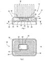
- Fig. 1 shows in section an electronic controller 10 for a vehicle fan with inter alia a heat sink 12, which is exposed to the air flow generated by the fan motor and is cooled by this.
- the regulator 10 has a power transistor 14, which is provided with a plastic housing 16, from which protrude three terminal contact elements 18 in the form of so-called "connection legs" in this case.
- a heat dissipation element 20 made of a metallic material, on which the actual semiconductor substrate 22 of the power transistor 14 is optionally electrically isolated (see Fig. 1 ).
- the terminal contact elements 18 are angled toward the outside of the housing 16 of the power transistor 14 facing away from the heat dissipation element 20 and are electrically connected at 24 to soldering surfaces of a printed circuit board 26 (not shown). Between the housing 16 and the printed circuit board 26 may be a flexible or otherwise elastic tolerance compensation element 28 for the purpose of tolerance compensation.
- the printed circuit board 26 is arranged within a cup-shaped part 30 of the heat sink 12, wherein this cup-shaped part 30 has a bottom portion 32 with peripheral upstanding edge 34. From the bottom portion 32 are a plurality of cooling fingers 36 from.
- the cup-shaped part 30 and the cooling fingers 36 of the heat sink 12 are formed integrally with each other.
- the peculiarity of the electronic regulator 10 described here and shown in the drawing consists in the manner of the thermal connection of the power transistor 14 to the heat sink 12.
- This thermal connection comprises a copper layer 38 which on the bottom portion 32 of the cup-shaped portion 30 of the heat sink 12th by thermal spraying and in particular by high velocity flame (cold gas) spraying.
- the heat sink 12 which consists of aluminum or an aluminum alloy, can now be soldered.
- a cohesive connection of the solderable heat removal element 20 with the heat sink 12 can now be realized by normal solder 40.
- soldering connection of the power transistor 14 on the one hand for the purpose of electrical connection to the printed circuit board 26 and on the other hand for thermal connection to the thermal sprayed copper layer 38 of the heat sink 12 is advantageously carried out by a vapor phase soldering, such as in EP-A-1 036 626 is described.
- a vapor phase soldering such as in EP-A-1 036 626 is described.
- the tolerance compensation element 28 between the housing 16 and the printed circuit board 26 is arranged.
- the contact surface of copper layer 38 and heat sink 12 is greater than the surface area of the copper layer 38, since the copper particles caused by the cold gas spraying due to high speed in the (soft) aluminum material of the heat sink 12 comparatively far penetrate into this and thus to enclose the near-vicinity copper particles comes through the aluminum material of the heat sink 12.
- Decisive for the embodiment is thus to have recognized that with a thermally sprayed copper layer 38 not only optimal heat transfer from the copper to the heat sink 12 but also a solderable coating of the heat sink 12 has created, to which now the heat dissipation element 20 of the transistor 14 itself can be thermally coupled optimally by soldering.
Landscapes
- Physics & Mathematics (AREA)
- Thermal Sciences (AREA)
- Engineering & Computer Science (AREA)
- Microelectronics & Electronic Packaging (AREA)
- Cooling Or The Like Of Semiconductors Or Solid State Devices (AREA)
- Cooling Or The Like Of Electrical Apparatus (AREA)
- Coating By Spraying Or Casting (AREA)
- Control Of Electric Motors In General (AREA)
Description
- Die Erfindung betrifft eine elektronische Einrichtung für insbesondere eine elektromechanische Anordnung und insbesondere einen elektronischen Regler für ein Fahrzeuggebläse.
- Leistungsregler oder andere elektronische (Leistungs-)Bauteile bedürfen der Kühlung, um vor thermischen Schäden geschützt zu sein. Zum Zwecke der Kühlung werden derartige elektronische Bauteile wie insbesondere Transistoren thermisch mit Kühlkörpern gekoppelt, die eine Wärmesenke bilden. Das zu kühlende elektronische Bauteil weist zu diesem Zweck ein Wärmeabführelement auf, das in thermischem Kontakt mit dem eigentlichen Halbleiterbauelement steht und an einer Seite des Gehäuses des Bauteils freiliegt. Dieses zu kühlende Wärmeabführelement kann auch zusätzlich als elektrisches Anschlusskontaktelement genutzt werden. Ferner ragen aus dem Gehäuse weitere Anschlusskontaktelemente heraus oder sind in der Außenseite des Gehäuses angeordnet. Das Wärmeabführelement ist mit dem Kühlkörper thermische verbunden, was zumeist mechanisch erfolgt, indem das Wärmeabführelement z.B. mittels einer Schraube an dem Kühlkörper festgeschraubt ist. Zwischen dem Wärmeabführelement und dem Kühlkörper kann noch eine Wärmeleitpaste o.dgl. Unebenheiten ausfüllendes thermisch leitendes Material angeordnet sein.
- Für den Betrieb eines zu kühlenden elektronischen Bauteils spielt der Wärmetransport zum Kühlkörper hin eine entscheidende Rolle. Der Wärmetransport auf Grund lediglich einer mechanischen Berührung von Wärmeabführelement und Kühlkörper ist nicht optimal. Wesentlich günstiger wäre es, wenn das Wärmeabführelement stoffschlüssig, beispielsweise durch Verlötung mit dem Kühlkörper verbunden ist. Dies allerdings setzt voraus, dass das Material des Kühlkörpers verlötbar ist. Zu diesem Zweck müsste der Kühlkörper beispielsweise aus Kupfer bestehen und nicht, wie bisher üblich, aus Aluminium oder einer Aluminiumlegierung. Die letztgenannten Materialien haben gegenüber Kupfer den Vorteil der geringeren spezifischen Wichte und der besseren thermischen Leitfähigkeit.
- Es ist aus
US-A-2002/0041506 bekannt, einen Transistor zwecks thermischer Kopplung mit einer Kupferplatte zu verlöten und diese Kupferplatte über eine thermisch leitende Zwischenschicht in Kontakt mit einem Kühlkörper zu bringen. - Der Erfindung liegt die Aufgabe zu Grunde, eine elektronische Einrichtung, insbesondere einen elektronischen Regler für eine elektromechanische Anordnung wie beispielsweise ein Fahrzeuggebläse zu schaffen, wobei als Kühlkörper für das zu kühlende elektronische Bauteil weiterhin ein leichtgewichtiges Material eingesetzt wird, der thermische Kontakt zwischen Bauteil und Kühlkörper aber verbessert ist.
- Zur Lösung dieser Aufgabe wird mit der Erfindung eine elektronische Einrichtung, insbesondere ein elektronischer Regler für eine elektromechanische Anordnung wie beispielsweise ein Fahrzeuggebläse vorgeschlagen, wobei die Einrichtung versehen ist mit den Merkmalen des Anspruchs 1; Weiterbildungen der Erfindung sind Gegenstand der Unteransprüche.
- Nach der Erfindung ist also vorgesehen, das zu kühlende Wärmeabführelement des elektronischen Bauteils stoffschlüssig mit einer Kupferschicht zu verbinden, die ihrerseits in thermischem Kontakt mit dem Kühlkörper steht. Durch die stoffschlüssige Anbindung des Wärmeabführelements mit der Kupferschicht, was beispielsweise und insbesondere durch eine Verlötung von Wärmeabführelement und Kupferschicht, aber auch durch eine Verklebung beider mittels eines thermisch leitenden Klebers erfolgt, kommt es zunächst einmal zu einer schnellen Verteilung der Wärme von dem Wärmeabführelement über die gesamte Fläche und Ausdehnung der Kupferschicht ("Wärmetransportaufspreizung"). Darüber hinaus erfolgt der Wärmetransport von dem Wärmeabführelement in die Kupferschicht auf Grund der stoffschlüssigen Verbindung beider Elemente extrem rasch. Die Erfindung ist also sowohl hinsichtlich eines verbesserten Wärmeabtransports vom Wärmeabführelement als auch hinsichtlich der Verteilung der abgeführten Wärme über die zweidimensionale Ausbreitung der Kupferschicht von Vorteil. Von der Kupferschicht erfolgt dann der Wärmetransport zum eigentlichen Kühlkörper infolge der thermischen Verbindung beider.
- Zur weiteren Verbesserung des Wärmetransports von der Kupferschicht zum Kühlkörper ist erfindungsgemäß vorgesehen, dass das Material der Kupferschicht durch thermisches Spritzen auf den Kühlkörper aufgebracht und infolge dieses Aufbringungsvorgangs mit dem Kühlkörper innig verbunden ist. Durch diesen Thermospritzvorgang kommt es zu einer ebenfalls stoffschlüssigen Verbindung zwischen der Kupferschicht und dem Kühlkörper, womit das gesamte für den Wärmeabtransport erforderliche Wärmetransportsystem aus einzelnen stoffschlüssig und damit bezüglich der Wärmeübergangswiderstände optimalen thermischen Verbindungen besteht.
- Es existieren unterschiedliche Verfahren zum thermischen Spritzen von Materialien auf Oberflächen. Vorteilhafterweise wird zur Aufbringung der Kupferschicht auf den Kühlkörper entweder ein Lichtbogenspritz-, oder ein Detonationsspritz-, oder ein Flammspritz-, insbesondere Hochgeschwindigkeits-Flammspritz- oder ein Plasmaspritzverfahren eingesetzt. Von besonderem Vorteil im Zusammenhang mit der Erfindung ist der Einsatz eines so genannten Kaltgasspritzverfahrens, wie es beispielsweise in
EP-A-0 911 425 ,EP-A-1 082 993 ,DE-A-41 41 020 ,DE-A-197 47 386 oderDE-A-100 37 212 beschrieben ist. Der Vorteil des Einsatzes des Kaltgasspritzens zum Aufbringen der Kupferschicht auf den Kühlkörper hat im Zusammenhang mit der Erfindung den Vorteil, dass die aufgespritzten Kupferpartikel auf Grund der vergleichsweise niedrigen Temperaturen nicht oxidieren und damit die Wärmeleitfähigkeit des Kupfers nicht leidet. Außerdem ist auf Grund der hohen Geschwindigkeiten, mit der die Kupferpartikel beim Kaltgasspritzen in das Substrat (hier den Kühlkörper) "eingeschossen" werden, eine hohe Materialdichte der Kupferschicht und eine gute Verkrallung der Kupferschicht in das vergleichsweise weiche Material des Kühlkörpers (im Regelfall Aluminium oder eine Aluminiumlegierung) gegeben. - In vorteilhafter Weiterbildung der Erfindung ist ferner vorgesehen, dass die Anschlusskontaktelemente des elektronischen Bauteils elektrisch und mechanisch mit den Anschlusskontaktfeldern einer Leiterplatine verbunden sind, die ihrerseits auf der dem Kühlkörper abgewandten Seite des elektronischen Bauteils angeordnet ist. Somit ist das elektronische Bauteil quasi "über Kopf" auf der Leiterplatine angeordnet; denn bisher werden die Wärmeabführkontakte von zu kühlenden elektronischen Bauelementen dann, wenn eine Metallisierung der Leiterplatine zur Abführung der Wärme eingesetzt wird, mit dem Abführelement auf der Platine aufliegend angeordnet. Die Verbindung des elektronischen Bauteils sowohl mit dem Kühlkörper als auch mit der Leiterplatine durch Verlötung erfolgt bei der zuvor beschriebenen Konstruktion zweckmäßigerweise durch eine Dampfphasenlötung.
- Zum Ausgleich von Toleranzen ist es von Vorteil, wenn zwischen dem Gehäuse des elektronischen Bauteils und der Leiterplatine ein elastisches Toleranzausgleichselement in Form eines flexiblen vorgebogenen Elements o.dgl. angeordnet ist.
- Die Erfindung wird nachfolgend anhand eines Ausführungsbeispiels unter Bezugnahme auf die Zeichnung näher erläutert. Im einzelnen zeigen dabei:
- Fig. 1
- einen Längsschnitt durch einen Kühlkörper mit thermisch mit diesem gekoppelten und elektrisch auf einer Leiterplatine angebundenen zu kühlenden elektrischen Bauteil und
- Fig. 2
- eine Ansicht entlang der Linie II-II der
Fig. 1 . -
Fig. 1 zeigt im Schnitt einen elektronischen Regler 10 für ein Fahrzeuggebläse mit unter anderem einem Kühlkörper 12, der der von dem Gebläsemotor erzeugten Luftströmung ausgesetzt ist und durch diese gekühlt wird. - Der Regler 10 weist einen Leistungstransistor 14 auf, der mit einem Kunststoffgehäuse 16 versehen ist, aus dem in diesem Fall drei Anschlusskontaktelemente 18 in Form von so genannten "Anschlussbeinchen" herausragen. Auf einer Seite des Gehäuses 16 wird dessen Außenfläche zumindest teilweise von einem Wärmeabführelement 20 aus einem metallischen Material gebildet, auf dem gegebenenfalls elektrisch isoliert das eigentliche Halbleitersubstrat 22 des Leistungstransistors 14 angeordnet ist (siehe
Fig. 1 ). Die Anschlusskontaktelemente 18 sind zu der dem Wärmeabführelement 20 abgewandten Außenseite des Gehäuses 16 des Leistungstransistors 14 hin abgewinkelt und bei 24 elektrisch mit (nicht gezeigten) Lötflächen einer Leiterplatine 26 verbunden. Zwischen dem Gehäuse 16 und der Leiterplatine 26 kann sich zwecks Toleranzausgleichs ein flexibles bzw. auf andere Weise elastisches Toleranzausgleichselement 28 befinden. - Die Leiterplatine 26 ist innerhalb eines napfförmigen Teils 30 des Kühlkörpers 12 angeordnet, wobei dieser napfförmige Teil 30 einen Bodenabschnitt 32 mit umlaufendem hochstehenden Rand 34 aufweist. Von dem Bodenabschnitt 32 stehen eine Vielzahl von Kühlfingern 36 ab. Der napfförmige Teil 30 und die Kühlfinger 36 des Kühlkörpers 12 sind einstückig miteinander ausgebildet.
- Die Besonderheit des hier beschriebenen und in der Zeichnung dargestellten elektronischen Reglers 10 besteht in der Art und Weise der thermischen Anbindung des Leistungstransistors 14 an den Kühlkörper 12. Diese thermische Anbindung umfasst eine Kupferschicht 38, die auf den Bodenabschnitt 32 des napfförmigen Teils 30 des Kühlkörpers 12 durch thermisches Spritzen und insbesondere durch Hochgeschwindigkeits-Flamm-(Kaltgas-)Spritzen aufgebracht ist. Durch diese Kupferschicht 38 wird nun der Kühlkörper 12, der aus Aluminium oder einer Aluminiumlegierung besteht, verlötbar. Somit lässt sich nun durch normales Lot 40 eine stoffschlüssige Verbindung des ebenfalls lötbaren Wärmeabführelements 20 mit dem Kühlkörper 12 realisieren.
- Die löttechnische Verbindung des Leistungstransistors 14 zum einen zwecks elektrischer Anbindung an die Leiterplatine 26 und zum anderen zwecks thermischer Anbindung an die thermische bespritzte Kupferschicht 38 des Kühlkörpers 12 erfolgt vorteilhafterweise durch eine Dampfphasenlötung, wie sie z.B. in
EP-A-1 036 626 beschrieben ist. Um bei diesem Prozess die Anschlusskontaktelemente 18 in einen für die Lötung zuverlässigen Kontakt mit der Leiterplatine 26 zu bringen, ist das Toleranzausgleichselement 28 zwischen dem Gehäuse 16 und der Leiterplatine 26 angeordnet. - Durch den extrem widerstandsarmen weil mittels der Verlötung 40 stoffschlüssigen thermischen Übergang zwischen dem Wärmeabführelement 20 und der Kupferschicht 38 kommt es zu einem extrem guten und damit auch schnellen Wärmetransport von dem Wärmeabführelement 20 in die Kupferschicht 38 hinein. In dieser Kupferschicht 38 verteilt sich nun die Wärme rasch in alle Richtungen, wodurch es zu einer "Aufspreizung" des Wärmetransportstroms innerhalb der Ebene, in der sich die Kupferschicht 38 erstreckt, kommt. Die auf diese Weise "aufgespreizte" Wärme gelangt nun wegen des großflächigen Kontakts der Kupferschicht 38 zum Kühlkörper 12 schnell in diesen hinein, wobei auch dieser Wärmeübergang denkbar widerstandsarm ist, da die Kupferschicht 38 stoffschlüssig mit dem Kühlkörper (hier dem Bodenabschnitt 32 des napfförmigen Teils 30 des Kühlkörpers 12) verbunden ist. Die Kontaktfläche von Kupferschicht 38 und Kühlkörper 12 ist größer als die Flächenausdehnung der Kupferschicht 38, da die Kupferpartikel durch das Kaltgasspritzen bedingt mit hoher Geschwindigkeit in das (weiche) Aluminium-Material des Kühlkörpers 12 vergleichsweise weit in diesen eindringen und es somit zu einem Umschließen der grenzschichtnahen Kupferpartikel durch das Aluminium-Material des Kühlkörpers 12 kommt. Entscheidend für das Ausführungsbeispiel ist also, erkannt zu haben, dass man mit einer thermisch gespritzten Kupferschicht 38 nicht nur einen optimalen Wärmeübergang vom Kupfer zum Kühlkörper 12 sondern auch eine lötfähige Beschichtung des Kühlkörpers 12 geschaffen hat, an den nun das Wärmeabführelement 20 des Transistors 14 sich durch Verlötung thermisch optimal ankoppeln lässt.
-
- 10
- Regler
- 12
- Kühlkörper
- 14
- Leistungstransistor
- 16
- Gehäuse
- 18
- Anschlusskontaktelement
- 20
- Wärmeabführelement
- 22
- Halbleitersubstrat
- 26
- Leiterplatine
- 28
- Toleranzausgleichselement
- 30
- napfförmiges Teil des Kühlkörpers
- 32
- Bodenabschnitt des napfförmigen Teils
- 34
- Rand des napfförmigen Teils
- 36
- Kühlfinger des Kühlkörpers
- 38
- Kupferschicht
- 40
- Lot
Claims (13)
- Elektronische Einrichtung, insbesondere elektronischer Regler für eine elektromechanische Anordnung wie z.B. ein Fahrzeuggebläse, mit- einem zu kühlenden elektronischen Bauteil (14), insbesondere einem Leistungsbauteil in Form eines Transistors, wobei das Bauteil (14) ein Gehäuse (16) mit einer Außenseite, an der mindestens ein Anschlusskontaktelement (18) und mindestens ein zu kühlendes Wärmeabführelement (20) zum Abführen von Wärme von dem Bauteil (14) angeordnet sind, und- einem mit dem Wärmeabführelement (20) thermisch verbundenen Kühlkörper (12),- wobei die thermische Verbindung zwischen dem Wärmeabführelement (20) des elektronischen Bauteils (14) und dem Kühlkörper (12) eine mit diesem thermisch gekoppelte Kupferschicht (38) aufweist und- wobei das Wärmeabführelement (20) mittels eines thermisch leitenden Materials (40) stoffschlüssig mit der Kupferschicht (38) verbunden ist,dadurch gekennzeichnet,- dass der Kühlkörper (12) Aluminium oder eine Aluminiumlegierung aufweist und- dass die Kupferschicht (38) durch thermisches Spritzen auf den Kühlkörper (12) aufgebracht und mit dem Kühlkörper (12) stoffschlüssig verbunden ist.
- Elektronische Einrichtung nach Anspruch 1, dadurch gekennzeichnet, dass die Kupferschicht (38) durch Lichtbogenspritzen, Detonationsspritzen, Flammspritzen, insbesondere Hochgeschwindigkeits-Flammspritzen, Plasmaspritzen oder Kaltgasspritzen auf den Kühlkörper (12) aufgebracht ist.
- Elektronische Einrichtung nach Anspruch 1 oder 2, dadurch gekennzeichnet, dass die thermische Kopplung ferner eine zwischen der Kupferschicht (38) und dem Kühlkörper (12) angeordnete thermisch leitende und elektrisch isolierende Isolationsschicht aufweist.
- Elektronische Einrichtung nach Anspruch 3, dadurch gekennzeichnet, dass die Kupferschicht (38) durch thermisches Spritzen auf die Isolationsschicht aufgebracht ist.
- Elektronische Einrichtung nach Anspruch 4, dadurch gekennzeichnet, dass die Kupferschicht (38) durch Lichtbogenspritzen, Detonationsspritzen, Flammspritzen, insbesondere Hochgeschwindigkeits-Flammspritzen, Plasmaspritzen oder Kaltgasspritzen auf die Isolationsschicht aufgebracht ist.
- Elektronische Einrichtung nach einem der Ansprüche 3 bis 5, dadurch gekennzeichnet, dass die Isolationsschicht keramisches Material aufweist.
- Elektronische Einrichtung nach Anspruch 6, dadurch gekennzeichnet, dass das keramische Material durch thermisches Spritzen auf den Kühlkörper (12) aufgebracht ist.
- Elektronische Einrichtung nach einem der Ansprüche 3 bis 7, dadurch gekennzeichnet, dass die Isolationsschicht mittels eines thermisch leitenden Klebers mit dem Kühlkörper (12) verbunden ist.
- Elektronische Einrichtung nach einem der Ansprüche 1 bis 8, dadurch gekennzeichnet, dass das thermische leitende Material (40) Lot ist.
- Elektronische Einrichtung nach einem der Ansprüche 1 bis 8, dadurch gekennzeichnet, dass das thermische leitende Material ein Kleber ist.
- Elektronische Einrichtung nach einem der Ansprüche 1 bis 10, dadurch gekennzeichnet, dass auf der dem Wärmeabführelement (20) gegenüberliegenden Seite des Gehäuses (16) des elektronischen Bauteils (14) eine Leiterplatine (26) angeordnet ist und dass das mindestens eine Anschlusskontaktelement (18) mit einem Anschlussfeld der Leiterplatine (26) mechanisch und elektrisch verbunden ist.
- Elektronische Einrichtung nach Anspruch 11, dadurch gekennzeichnet, dass zwischen der Leiterplatine (26) und dem Gehäuse (16) des elektronischen Bauteils (14) ein elastisches Toleranzausgleichselement (28) angeordnet ist.
- Elektronische Einrichtung nach einem der Ansprüche 1 bis 12, dadurch gekennzeichnet, dass das Wärmeabführelement (20) auch der elektrischen Kontaktierung des elektronischen Bauteils (14) dient.
Applications Claiming Priority (2)
| Application Number | Priority Date | Filing Date | Title |
|---|---|---|---|
| DE10234586 | 2002-07-30 | ||
| DE10234586 | 2002-07-30 |
Publications (3)
| Publication Number | Publication Date |
|---|---|
| EP1387609A2 EP1387609A2 (de) | 2004-02-04 |
| EP1387609A3 EP1387609A3 (de) | 2005-07-20 |
| EP1387609B1 true EP1387609B1 (de) | 2008-11-12 |
Family
ID=30010504
Family Applications (1)
| Application Number | Title | Priority Date | Filing Date |
|---|---|---|---|
| EP03017143A Expired - Lifetime EP1387609B1 (de) | 2002-07-30 | 2003-07-29 | Elektronische Einrichtung, insbesondere elektronische Regler für eine elektromechanische Anordnung wie beispielsweise ein Fahrzeuggebläse |
Country Status (4)
| Country | Link |
|---|---|
| EP (1) | EP1387609B1 (de) |
| AT (1) | ATE414403T1 (de) |
| DE (1) | DE50310772D1 (de) |
| ES (1) | ES2315446T3 (de) |
Families Citing this family (11)
| Publication number | Priority date | Publication date | Assignee | Title |
|---|---|---|---|---|
| JP3850413B2 (ja) * | 2004-02-16 | 2006-11-29 | 株式会社ソニー・コンピュータエンタテインメント | 電子デバイス冷却装置、電子デバイス冷却方法、電子デバイス冷却制御プログラム及びそれを格納した記録媒体 |
| DE102004054063B3 (de) * | 2004-11-05 | 2006-06-08 | Danfoss Silicon Power Gmbh | Verfahren zum Herstellen einer rissarmen Verbindung und rissarme Verbindung |
| DE102004055817B3 (de) * | 2004-11-18 | 2006-01-12 | Danfoss Silicon Power Gmbh | Verfahren zum Herstellen eines Leistungshalbleitermoduls und Halbleitermodul |
| DE102005022226B4 (de) * | 2005-05-10 | 2008-05-15 | RUNGE, André | Kühlanordnung für in einem Gehäuse angeordnete elektronische Bauelemente |
| EP1833088A1 (de) | 2006-03-07 | 2007-09-12 | Danfoss Silicon Power GmbH | Verfahren zur Erstellung einer rissarmer Verbindung zwischen einer Wärmesenke und einer Substratplatte |
| JP4241859B2 (ja) | 2007-07-19 | 2009-03-18 | トヨタ自動車株式会社 | パワーモジュールの製造方法、パワーモジュール、車両用インバータ、及び車両 |
| DE102009042518A1 (de) * | 2009-09-16 | 2011-03-24 | Esw Gmbh | Vorrichtung zur Kühlung von Halbleitern |
| DE102009047703A1 (de) * | 2009-12-09 | 2011-06-16 | Robert Bosch Gmbh | Befestigungsanordnung für leiterplattenmontierte Bauteile mit verbessertem Kühlkonzept |
| EP3131377A1 (de) | 2015-08-14 | 2017-02-15 | Siemens Aktiengesellschaft | Phasenmodul für einen stromrichter |
| CN108541193A (zh) * | 2018-05-31 | 2018-09-14 | 湖北省雄雄电子科技有限公司 | 一种新型的电动车控制器 |
| DE102021201248B4 (de) * | 2021-02-10 | 2025-03-27 | Vitesco Technologies Germany Gmbh | Steuermodul für ein Fahrzeug mit mindestens einem Elektromotor und einem Getriebe |
Family Cites Families (4)
| Publication number | Priority date | Publication date | Assignee | Title |
|---|---|---|---|---|
| DE4337866A1 (de) * | 1993-11-05 | 1995-05-11 | Siemens Ag | Steuergerät, insbesondere für ein Kraftfahrzeug |
| DE19943409A1 (de) * | 1999-09-10 | 2001-03-15 | Linde Gas Ag | Verbund aus einer Kompositmembran |
| FR2805961A1 (fr) * | 2000-03-06 | 2001-09-07 | Sagem | Module electrique de puissance et procedes pour sa fabrication |
| TWI282656B (en) * | 2000-08-29 | 2007-06-11 | Delta Electronics Inc | A small power supply apparatus capable of increasing heat sink and preventing over current load |
-
2003
- 2003-07-29 EP EP03017143A patent/EP1387609B1/de not_active Expired - Lifetime
- 2003-07-29 DE DE50310772T patent/DE50310772D1/de not_active Expired - Lifetime
- 2003-07-29 ES ES03017143T patent/ES2315446T3/es not_active Expired - Lifetime
- 2003-07-29 AT AT03017143T patent/ATE414403T1/de not_active IP Right Cessation
Also Published As
| Publication number | Publication date |
|---|---|
| EP1387609A2 (de) | 2004-02-04 |
| DE50310772D1 (de) | 2008-12-24 |
| ATE414403T1 (de) | 2008-11-15 |
| EP1387609A3 (de) | 2005-07-20 |
| ES2315446T3 (es) | 2009-04-01 |
Similar Documents
| Publication | Publication Date | Title |
|---|---|---|
| DE102004018469B3 (de) | Leistungshalbleiterschaltung | |
| EP1450404B1 (de) | Anordnung in Druckkontaktierung mit einem Leistungshalbleitermodul | |
| DE102008048005B3 (de) | Leistungshalbleitermodulanordnung und Verfahren zur Herstellung einer Leistungshalbleitermodulanordnung | |
| DE112014001487B4 (de) | Halbleitermodul | |
| EP0805494B1 (de) | Halbleiterleistungsmodul hoher Packungsdichte in Mehrschichtbauweise | |
| EP0931346B1 (de) | Mikroelektronisches bauteil in sandwich-bauweise | |
| DE102009002191A1 (de) | Leistungshalbleitermodul, Leistungshalbleitermodulanordnung und Verfahren zur Herstellung einer Leistungshalbleitermodulanordnung | |
| EP1713124A2 (de) | Leistungshalbleitermodul mit Verbindungsbahnen und mit Anschlusselementen, deren Verbindung zu den Verbindungsbahnen stoffbündig ausgebildet ist. | |
| WO2014135373A1 (de) | Elektronische, optoelektronische oder elektrische anordnung | |
| EP3405975A1 (de) | Vorrichtung zur kühlung mindestens einer stromschiene und korrespondierende leistungsschaltung | |
| DE112016007562B4 (de) | Halbleitervorrichtung | |
| CH668667A5 (de) | Leistungshalbleitermodul. | |
| EP1387609A2 (de) | Elektronische Einrichtung, insbesondere elektronische Regler für eine elektromechanische Anordnung wie beispielsweise ein Fahrzeuggebläse | |
| WO2018184948A1 (de) | Zweiseitig gekühlter schaltkreis | |
| DE19859739A1 (de) | Kühlvorrichtung, insbesondere zur Verwendung in einem elektronischen Steuergerät | |
| DE102015210061A1 (de) | Verfahren zur elektrischen Kontaktierung eines Bauteils und Bauteilmodul | |
| EP3226269B1 (de) | Leistungshalbleitereinrichtung | |
| EP1265282A2 (de) | Schaltungsanordnung | |
| EP1455391B1 (de) | Leistungshalbleitermodul mit Sensorikbauteil | |
| DE102004030443A1 (de) | Steuergerät | |
| DE102005050534A1 (de) | Leistungshalbleitermodul | |
| DE102006011995B3 (de) | Leistungshalbleitermodul mit segmentierter Grundplatte | |
| EP2006910B1 (de) | Leistungselektronikmodul | |
| DE102017211336A1 (de) | Leistungsmodul mit oberflächenmontierten elektrischen Kontaktierungselementen | |
| DE10149774A1 (de) | Verfahren zum Verpacken von elektronischen Baugruppen und Mehrfachchipverpackung |
Legal Events
| Date | Code | Title | Description |
|---|---|---|---|
| PUAI | Public reference made under article 153(3) epc to a published international application that has entered the european phase |
Free format text: ORIGINAL CODE: 0009012 |
|
| AK | Designated contracting states |
Kind code of ref document: A2 Designated state(s): AT BE BG CH CY CZ DE DK EE ES FI FR GB GR HU IE IT LI LU MC NL PT RO SE SI SK TR |
|
| AX | Request for extension of the european patent |
Extension state: AL LT LV MK |
|
| PUAL | Search report despatched |
Free format text: ORIGINAL CODE: 0009013 |
|
| AK | Designated contracting states |
Kind code of ref document: A3 Designated state(s): AT BE BG CH CY CZ DE DK EE ES FI FR GB GR HU IE IT LI LU MC NL PT RO SE SI SK TR |
|
| AX | Request for extension of the european patent |
Extension state: AL LT LV MK |
|
| 17P | Request for examination filed |
Effective date: 20051209 |
|
| AKX | Designation fees paid |
Designated state(s): AT BE BG CH CY CZ DE DK EE ES FI FR GB GR HU IE IT LI LU MC NL PT RO SE SI SK TR |
|
| 17Q | First examination report despatched |
Effective date: 20070601 |
|
| GRAP | Despatch of communication of intention to grant a patent |
Free format text: ORIGINAL CODE: EPIDOSNIGR1 |
|
| GRAS | Grant fee paid |
Free format text: ORIGINAL CODE: EPIDOSNIGR3 |
|
| GRAA | (expected) grant |
Free format text: ORIGINAL CODE: 0009210 |
|
| AK | Designated contracting states |
Kind code of ref document: B1 Designated state(s): AT BE BG CH CY CZ DE DK EE ES FI FR GB GR HU IE IT LI LU MC NL PT RO SE SI SK TR |
|
| REG | Reference to a national code |
Ref country code: GB Ref legal event code: FG4D Free format text: NOT ENGLISH |
|
| REG | Reference to a national code |
Ref country code: CH Ref legal event code: EP |
|
| REG | Reference to a national code |
Ref country code: IE Ref legal event code: FG4D Free format text: LANGUAGE OF EP DOCUMENT: GERMAN |
|
| REF | Corresponds to: |
Ref document number: 50310772 Country of ref document: DE Date of ref document: 20081224 Kind code of ref document: P |
|
| REG | Reference to a national code |
Ref country code: SE Ref legal event code: TRGR |
|
| REG | Reference to a national code |
Ref country code: ES Ref legal event code: FG2A Ref document number: 2315446 Country of ref document: ES Kind code of ref document: T3 |
|
| NLV1 | Nl: lapsed or annulled due to failure to fulfill the requirements of art. 29p and 29m of the patents act | ||
| PG25 | Lapsed in a contracting state [announced via postgrant information from national office to epo] |
Ref country code: NL Free format text: LAPSE BECAUSE OF FAILURE TO SUBMIT A TRANSLATION OF THE DESCRIPTION OR TO PAY THE FEE WITHIN THE PRESCRIBED TIME-LIMIT Effective date: 20081112 Ref country code: FI Free format text: LAPSE BECAUSE OF FAILURE TO SUBMIT A TRANSLATION OF THE DESCRIPTION OR TO PAY THE FEE WITHIN THE PRESCRIBED TIME-LIMIT Effective date: 20081112 Ref country code: SI Free format text: LAPSE BECAUSE OF FAILURE TO SUBMIT A TRANSLATION OF THE DESCRIPTION OR TO PAY THE FEE WITHIN THE PRESCRIBED TIME-LIMIT Effective date: 20081112 |
|
| REG | Reference to a national code |
Ref country code: IE Ref legal event code: FD4D |
|
| PG25 | Lapsed in a contracting state [announced via postgrant information from national office to epo] |
Ref country code: EE Free format text: LAPSE BECAUSE OF FAILURE TO SUBMIT A TRANSLATION OF THE DESCRIPTION OR TO PAY THE FEE WITHIN THE PRESCRIBED TIME-LIMIT Effective date: 20081112 Ref country code: BG Free format text: LAPSE BECAUSE OF FAILURE TO SUBMIT A TRANSLATION OF THE DESCRIPTION OR TO PAY THE FEE WITHIN THE PRESCRIBED TIME-LIMIT Effective date: 20090212 Ref country code: RO Free format text: LAPSE BECAUSE OF FAILURE TO SUBMIT A TRANSLATION OF THE DESCRIPTION OR TO PAY THE FEE WITHIN THE PRESCRIBED TIME-LIMIT Effective date: 20081112 Ref country code: DK Free format text: LAPSE BECAUSE OF FAILURE TO SUBMIT A TRANSLATION OF THE DESCRIPTION OR TO PAY THE FEE WITHIN THE PRESCRIBED TIME-LIMIT Effective date: 20081112 Ref country code: IE Free format text: LAPSE BECAUSE OF FAILURE TO SUBMIT A TRANSLATION OF THE DESCRIPTION OR TO PAY THE FEE WITHIN THE PRESCRIBED TIME-LIMIT Effective date: 20081112 |
|
| PG25 | Lapsed in a contracting state [announced via postgrant information from national office to epo] |
Ref country code: PT Free format text: LAPSE BECAUSE OF FAILURE TO SUBMIT A TRANSLATION OF THE DESCRIPTION OR TO PAY THE FEE WITHIN THE PRESCRIBED TIME-LIMIT Effective date: 20090413 Ref country code: CZ Free format text: LAPSE BECAUSE OF FAILURE TO SUBMIT A TRANSLATION OF THE DESCRIPTION OR TO PAY THE FEE WITHIN THE PRESCRIBED TIME-LIMIT Effective date: 20081112 |
|
| PLBE | No opposition filed within time limit |
Free format text: ORIGINAL CODE: 0009261 |
|
| STAA | Information on the status of an ep patent application or granted ep patent |
Free format text: STATUS: NO OPPOSITION FILED WITHIN TIME LIMIT |
|
| PG25 | Lapsed in a contracting state [announced via postgrant information from national office to epo] |
Ref country code: SK Free format text: LAPSE BECAUSE OF FAILURE TO SUBMIT A TRANSLATION OF THE DESCRIPTION OR TO PAY THE FEE WITHIN THE PRESCRIBED TIME-LIMIT Effective date: 20081112 |
|
| 26N | No opposition filed |
Effective date: 20090813 |
|
| BERE | Be: lapsed |
Owner name: BEHR-HELLA THERMOCONTROL G.M.B.H. Effective date: 20090731 |
|
| PG25 | Lapsed in a contracting state [announced via postgrant information from national office to epo] |
Ref country code: MC Free format text: LAPSE BECAUSE OF NON-PAYMENT OF DUE FEES Effective date: 20090731 |
|
| REG | Reference to a national code |
Ref country code: CH Ref legal event code: PL |
|
| PG25 | Lapsed in a contracting state [announced via postgrant information from national office to epo] |
Ref country code: LI Free format text: LAPSE BECAUSE OF NON-PAYMENT OF DUE FEES Effective date: 20090731 Ref country code: CH Free format text: LAPSE BECAUSE OF NON-PAYMENT OF DUE FEES Effective date: 20090731 |
|
| PG25 | Lapsed in a contracting state [announced via postgrant information from national office to epo] |
Ref country code: BE Free format text: LAPSE BECAUSE OF NON-PAYMENT OF DUE FEES Effective date: 20090731 |
|
| PG25 | Lapsed in a contracting state [announced via postgrant information from national office to epo] |
Ref country code: GR Free format text: LAPSE BECAUSE OF FAILURE TO SUBMIT A TRANSLATION OF THE DESCRIPTION OR TO PAY THE FEE WITHIN THE PRESCRIBED TIME-LIMIT Effective date: 20090213 |
|
| PG25 | Lapsed in a contracting state [announced via postgrant information from national office to epo] |
Ref country code: AT Free format text: LAPSE BECAUSE OF NON-PAYMENT OF DUE FEES Effective date: 20090729 |
|
| PG25 | Lapsed in a contracting state [announced via postgrant information from national office to epo] |
Ref country code: LU Free format text: LAPSE BECAUSE OF NON-PAYMENT OF DUE FEES Effective date: 20090729 |
|
| PG25 | Lapsed in a contracting state [announced via postgrant information from national office to epo] |
Ref country code: HU Free format text: LAPSE BECAUSE OF FAILURE TO SUBMIT A TRANSLATION OF THE DESCRIPTION OR TO PAY THE FEE WITHIN THE PRESCRIBED TIME-LIMIT Effective date: 20090513 |
|
| PG25 | Lapsed in a contracting state [announced via postgrant information from national office to epo] |
Ref country code: TR Free format text: LAPSE BECAUSE OF FAILURE TO SUBMIT A TRANSLATION OF THE DESCRIPTION OR TO PAY THE FEE WITHIN THE PRESCRIBED TIME-LIMIT Effective date: 20081112 |
|
| PG25 | Lapsed in a contracting state [announced via postgrant information from national office to epo] |
Ref country code: CY Free format text: LAPSE BECAUSE OF FAILURE TO SUBMIT A TRANSLATION OF THE DESCRIPTION OR TO PAY THE FEE WITHIN THE PRESCRIBED TIME-LIMIT Effective date: 20081112 |
|
| REG | Reference to a national code |
Ref country code: FR Ref legal event code: PLFP Year of fee payment: 14 |
|
| REG | Reference to a national code |
Ref country code: FR Ref legal event code: PLFP Year of fee payment: 15 |
|
| REG | Reference to a national code |
Ref country code: FR Ref legal event code: PLFP Year of fee payment: 16 |
|
| REG | Reference to a national code |
Ref country code: DE Ref legal event code: R081 Ref document number: 50310772 Country of ref document: DE Owner name: BEHR-HELLA THERMOCONTROL GMBH, DE Free format text: FORMER OWNER: BEHR-HELLA THERMOCONTROL GMBH, 70469 STUTTGART, DE |
|
| PGFP | Annual fee paid to national office [announced via postgrant information from national office to epo] |
Ref country code: SE Payment date: 20220721 Year of fee payment: 20 Ref country code: IT Payment date: 20220729 Year of fee payment: 20 Ref country code: GB Payment date: 20220725 Year of fee payment: 20 Ref country code: ES Payment date: 20220819 Year of fee payment: 20 Ref country code: DE Payment date: 20220621 Year of fee payment: 20 |
|
| PGFP | Annual fee paid to national office [announced via postgrant information from national office to epo] |
Ref country code: FR Payment date: 20220726 Year of fee payment: 20 |
|
| P01 | Opt-out of the competence of the unified patent court (upc) registered |
Effective date: 20230524 |
|
| REG | Reference to a national code |
Ref country code: DE Ref legal event code: R071 Ref document number: 50310772 Country of ref document: DE |
|
| REG | Reference to a national code |
Ref country code: ES Ref legal event code: FD2A Effective date: 20230804 |
|
| P02 | Opt-out of the competence of the unified patent court (upc) changed |
Effective date: 20230711 |
|
| REG | Reference to a national code |
Ref country code: GB Ref legal event code: PE20 Expiry date: 20230728 |
|
| REG | Reference to a national code |
Ref country code: SE Ref legal event code: EUG |
|
| PG25 | Lapsed in a contracting state [announced via postgrant information from national office to epo] |
Ref country code: GB Free format text: LAPSE BECAUSE OF EXPIRATION OF PROTECTION Effective date: 20230728 Ref country code: ES Free format text: LAPSE BECAUSE OF EXPIRATION OF PROTECTION Effective date: 20230730 |