EP1387417A2 - Manufacturing method for monolithic piezoelectric part, and monolithic piezoelectric part - Google Patents
Manufacturing method for monolithic piezoelectric part, and monolithic piezoelectric part Download PDFInfo
- Publication number
- EP1387417A2 EP1387417A2 EP03016741A EP03016741A EP1387417A2 EP 1387417 A2 EP1387417 A2 EP 1387417A2 EP 03016741 A EP03016741 A EP 03016741A EP 03016741 A EP03016741 A EP 03016741A EP 1387417 A2 EP1387417 A2 EP 1387417A2
- Authority
- EP
- European Patent Office
- Prior art keywords
- piezoelectric
- ceramic
- site component
- raw material
- monolithic
- Prior art date
- Legal status (The legal status is an assumption and is not a legal conclusion. Google has not performed a legal analysis and makes no representation as to the accuracy of the status listed.)
- Granted
Links
Images


Classifications
-
- H—ELECTRICITY
- H10—SEMICONDUCTOR DEVICES; ELECTRIC SOLID-STATE DEVICES NOT OTHERWISE PROVIDED FOR
- H10N—ELECTRIC SOLID-STATE DEVICES NOT OTHERWISE PROVIDED FOR
- H10N30/00—Piezoelectric or electrostrictive devices
- H10N30/50—Piezoelectric or electrostrictive devices having a stacked or multilayer structure
-
- C—CHEMISTRY; METALLURGY
- C04—CEMENTS; CONCRETE; ARTIFICIAL STONE; CERAMICS; REFRACTORIES
- C04B—LIME, MAGNESIA; SLAG; CEMENTS; COMPOSITIONS THEREOF, e.g. MORTARS, CONCRETE OR LIKE BUILDING MATERIALS; ARTIFICIAL STONE; CERAMICS; REFRACTORIES; TREATMENT OF NATURAL STONE
- C04B35/00—Shaped ceramic products characterised by their composition; Ceramics compositions; Processing powders of inorganic compounds preparatory to the manufacturing of ceramic products
- C04B35/01—Shaped ceramic products characterised by their composition; Ceramics compositions; Processing powders of inorganic compounds preparatory to the manufacturing of ceramic products based on oxide ceramics
- C04B35/48—Shaped ceramic products characterised by their composition; Ceramics compositions; Processing powders of inorganic compounds preparatory to the manufacturing of ceramic products based on oxide ceramics based on zirconium or hafnium oxides, zirconates, zircon or hafnates
- C04B35/49—Shaped ceramic products characterised by their composition; Ceramics compositions; Processing powders of inorganic compounds preparatory to the manufacturing of ceramic products based on oxide ceramics based on zirconium or hafnium oxides, zirconates, zircon or hafnates containing also titanium oxides or titanates
- C04B35/491—Shaped ceramic products characterised by their composition; Ceramics compositions; Processing powders of inorganic compounds preparatory to the manufacturing of ceramic products based on oxide ceramics based on zirconium or hafnium oxides, zirconates, zircon or hafnates containing also titanium oxides or titanates based on lead zirconates and lead titanates, e.g. PZT
- C04B35/493—Shaped ceramic products characterised by their composition; Ceramics compositions; Processing powders of inorganic compounds preparatory to the manufacturing of ceramic products based on oxide ceramics based on zirconium or hafnium oxides, zirconates, zircon or hafnates containing also titanium oxides or titanates based on lead zirconates and lead titanates, e.g. PZT containing also other lead compounds
-
- H—ELECTRICITY
- H10—SEMICONDUCTOR DEVICES; ELECTRIC SOLID-STATE DEVICES NOT OTHERWISE PROVIDED FOR
- H10N—ELECTRIC SOLID-STATE DEVICES NOT OTHERWISE PROVIDED FOR
- H10N30/00—Piezoelectric or electrostrictive devices
- H10N30/01—Manufacture or treatment
- H10N30/05—Manufacture of multilayered piezoelectric or electrostrictive devices, or parts thereof, e.g. by stacking piezoelectric bodies and electrodes
- H10N30/053—Manufacture of multilayered piezoelectric or electrostrictive devices, or parts thereof, e.g. by stacking piezoelectric bodies and electrodes by integrally sintering piezoelectric or electrostrictive bodies and electrodes
-
- H—ELECTRICITY
- H10—SEMICONDUCTOR DEVICES; ELECTRIC SOLID-STATE DEVICES NOT OTHERWISE PROVIDED FOR
- H10N—ELECTRIC SOLID-STATE DEVICES NOT OTHERWISE PROVIDED FOR
- H10N30/00—Piezoelectric or electrostrictive devices
- H10N30/80—Constructional details
- H10N30/85—Piezoelectric or electrostrictive active materials
- H10N30/853—Ceramic compositions
- H10N30/8548—Lead-based oxides
- H10N30/8554—Lead-zirconium titanate [PZT] based
-
- C—CHEMISTRY; METALLURGY
- C04—CEMENTS; CONCRETE; ARTIFICIAL STONE; CERAMICS; REFRACTORIES
- C04B—LIME, MAGNESIA; SLAG; CEMENTS; COMPOSITIONS THEREOF, e.g. MORTARS, CONCRETE OR LIKE BUILDING MATERIALS; ARTIFICIAL STONE; CERAMICS; REFRACTORIES; TREATMENT OF NATURAL STONE
- C04B2235/00—Aspects relating to ceramic starting mixtures or sintered ceramic products
- C04B2235/02—Composition of constituents of the starting material or of secondary phases of the final product
- C04B2235/30—Constituents and secondary phases not being of a fibrous nature
- C04B2235/32—Metal oxides, mixed metal oxides, or oxide-forming salts thereof, e.g. carbonates, nitrates, (oxy)hydroxides, chlorides
- C04B2235/3205—Alkaline earth oxides or oxide forming salts thereof, e.g. beryllium oxide
- C04B2235/3206—Magnesium oxides or oxide-forming salts thereof
-
- C—CHEMISTRY; METALLURGY
- C04—CEMENTS; CONCRETE; ARTIFICIAL STONE; CERAMICS; REFRACTORIES
- C04B—LIME, MAGNESIA; SLAG; CEMENTS; COMPOSITIONS THEREOF, e.g. MORTARS, CONCRETE OR LIKE BUILDING MATERIALS; ARTIFICIAL STONE; CERAMICS; REFRACTORIES; TREATMENT OF NATURAL STONE
- C04B2235/00—Aspects relating to ceramic starting mixtures or sintered ceramic products
- C04B2235/02—Composition of constituents of the starting material or of secondary phases of the final product
- C04B2235/30—Constituents and secondary phases not being of a fibrous nature
- C04B2235/32—Metal oxides, mixed metal oxides, or oxide-forming salts thereof, e.g. carbonates, nitrates, (oxy)hydroxides, chlorides
- C04B2235/3231—Refractory metal oxides, their mixed metal oxides, or oxide-forming salts thereof
- C04B2235/3241—Chromium oxides, chromates, or oxide-forming salts thereof
-
- C—CHEMISTRY; METALLURGY
- C04—CEMENTS; CONCRETE; ARTIFICIAL STONE; CERAMICS; REFRACTORIES
- C04B—LIME, MAGNESIA; SLAG; CEMENTS; COMPOSITIONS THEREOF, e.g. MORTARS, CONCRETE OR LIKE BUILDING MATERIALS; ARTIFICIAL STONE; CERAMICS; REFRACTORIES; TREATMENT OF NATURAL STONE
- C04B2235/00—Aspects relating to ceramic starting mixtures or sintered ceramic products
- C04B2235/02—Composition of constituents of the starting material or of secondary phases of the final product
- C04B2235/30—Constituents and secondary phases not being of a fibrous nature
- C04B2235/32—Metal oxides, mixed metal oxides, or oxide-forming salts thereof, e.g. carbonates, nitrates, (oxy)hydroxides, chlorides
- C04B2235/3231—Refractory metal oxides, their mixed metal oxides, or oxide-forming salts thereof
- C04B2235/3251—Niobium oxides, niobates, tantalum oxides, tantalates, or oxide-forming salts thereof
-
- C—CHEMISTRY; METALLURGY
- C04—CEMENTS; CONCRETE; ARTIFICIAL STONE; CERAMICS; REFRACTORIES
- C04B—LIME, MAGNESIA; SLAG; CEMENTS; COMPOSITIONS THEREOF, e.g. MORTARS, CONCRETE OR LIKE BUILDING MATERIALS; ARTIFICIAL STONE; CERAMICS; REFRACTORIES; TREATMENT OF NATURAL STONE
- C04B2235/00—Aspects relating to ceramic starting mixtures or sintered ceramic products
- C04B2235/02—Composition of constituents of the starting material or of secondary phases of the final product
- C04B2235/30—Constituents and secondary phases not being of a fibrous nature
- C04B2235/32—Metal oxides, mixed metal oxides, or oxide-forming salts thereof, e.g. carbonates, nitrates, (oxy)hydroxides, chlorides
- C04B2235/3231—Refractory metal oxides, their mixed metal oxides, or oxide-forming salts thereof
- C04B2235/3258—Tungsten oxides, tungstates, or oxide-forming salts thereof
-
- C—CHEMISTRY; METALLURGY
- C04—CEMENTS; CONCRETE; ARTIFICIAL STONE; CERAMICS; REFRACTORIES
- C04B—LIME, MAGNESIA; SLAG; CEMENTS; COMPOSITIONS THEREOF, e.g. MORTARS, CONCRETE OR LIKE BUILDING MATERIALS; ARTIFICIAL STONE; CERAMICS; REFRACTORIES; TREATMENT OF NATURAL STONE
- C04B2235/00—Aspects relating to ceramic starting mixtures or sintered ceramic products
- C04B2235/02—Composition of constituents of the starting material or of secondary phases of the final product
- C04B2235/30—Constituents and secondary phases not being of a fibrous nature
- C04B2235/32—Metal oxides, mixed metal oxides, or oxide-forming salts thereof, e.g. carbonates, nitrates, (oxy)hydroxides, chlorides
- C04B2235/327—Iron group oxides, their mixed metal oxides, or oxide-forming salts thereof
- C04B2235/3275—Cobalt oxides, cobaltates or cobaltites or oxide forming salts thereof, e.g. bismuth cobaltate, zinc cobaltite
-
- C—CHEMISTRY; METALLURGY
- C04—CEMENTS; CONCRETE; ARTIFICIAL STONE; CERAMICS; REFRACTORIES
- C04B—LIME, MAGNESIA; SLAG; CEMENTS; COMPOSITIONS THEREOF, e.g. MORTARS, CONCRETE OR LIKE BUILDING MATERIALS; ARTIFICIAL STONE; CERAMICS; REFRACTORIES; TREATMENT OF NATURAL STONE
- C04B2235/00—Aspects relating to ceramic starting mixtures or sintered ceramic products
- C04B2235/02—Composition of constituents of the starting material or of secondary phases of the final product
- C04B2235/30—Constituents and secondary phases not being of a fibrous nature
- C04B2235/32—Metal oxides, mixed metal oxides, or oxide-forming salts thereof, e.g. carbonates, nitrates, (oxy)hydroxides, chlorides
- C04B2235/327—Iron group oxides, their mixed metal oxides, or oxide-forming salts thereof
- C04B2235/3279—Nickel oxides, nickalates, or oxide-forming salts thereof
-
- C—CHEMISTRY; METALLURGY
- C04—CEMENTS; CONCRETE; ARTIFICIAL STONE; CERAMICS; REFRACTORIES
- C04B—LIME, MAGNESIA; SLAG; CEMENTS; COMPOSITIONS THEREOF, e.g. MORTARS, CONCRETE OR LIKE BUILDING MATERIALS; ARTIFICIAL STONE; CERAMICS; REFRACTORIES; TREATMENT OF NATURAL STONE
- C04B2235/00—Aspects relating to ceramic starting mixtures or sintered ceramic products
- C04B2235/02—Composition of constituents of the starting material or of secondary phases of the final product
- C04B2235/30—Constituents and secondary phases not being of a fibrous nature
- C04B2235/32—Metal oxides, mixed metal oxides, or oxide-forming salts thereof, e.g. carbonates, nitrates, (oxy)hydroxides, chlorides
- C04B2235/3294—Antimony oxides, antimonates, antimonites or oxide forming salts thereof, indium antimonate
-
- C—CHEMISTRY; METALLURGY
- C04—CEMENTS; CONCRETE; ARTIFICIAL STONE; CERAMICS; REFRACTORIES
- C04B—LIME, MAGNESIA; SLAG; CEMENTS; COMPOSITIONS THEREOF, e.g. MORTARS, CONCRETE OR LIKE BUILDING MATERIALS; ARTIFICIAL STONE; CERAMICS; REFRACTORIES; TREATMENT OF NATURAL STONE
- C04B2235/00—Aspects relating to ceramic starting mixtures or sintered ceramic products
- C04B2235/60—Aspects relating to the preparation, properties or mechanical treatment of green bodies or pre-forms
- C04B2235/602—Making the green bodies or pre-forms by moulding
- C04B2235/6025—Tape casting, e.g. with a doctor blade
-
- C—CHEMISTRY; METALLURGY
- C04—CEMENTS; CONCRETE; ARTIFICIAL STONE; CERAMICS; REFRACTORIES
- C04B—LIME, MAGNESIA; SLAG; CEMENTS; COMPOSITIONS THEREOF, e.g. MORTARS, CONCRETE OR LIKE BUILDING MATERIALS; ARTIFICIAL STONE; CERAMICS; REFRACTORIES; TREATMENT OF NATURAL STONE
- C04B2235/00—Aspects relating to ceramic starting mixtures or sintered ceramic products
- C04B2235/65—Aspects relating to heat treatments of ceramic bodies such as green ceramics or pre-sintered ceramics, e.g. burning, sintering or melting processes
- C04B2235/656—Aspects relating to heat treatments of ceramic bodies such as green ceramics or pre-sintered ceramics, e.g. burning, sintering or melting processes characterised by specific heating conditions during heat treatment
-
- C—CHEMISTRY; METALLURGY
- C04—CEMENTS; CONCRETE; ARTIFICIAL STONE; CERAMICS; REFRACTORIES
- C04B—LIME, MAGNESIA; SLAG; CEMENTS; COMPOSITIONS THEREOF, e.g. MORTARS, CONCRETE OR LIKE BUILDING MATERIALS; ARTIFICIAL STONE; CERAMICS; REFRACTORIES; TREATMENT OF NATURAL STONE
- C04B2235/00—Aspects relating to ceramic starting mixtures or sintered ceramic products
- C04B2235/65—Aspects relating to heat treatments of ceramic bodies such as green ceramics or pre-sintered ceramics, e.g. burning, sintering or melting processes
- C04B2235/658—Atmosphere during thermal treatment
- C04B2235/6583—Oxygen containing atmosphere, e.g. with changing oxygen pressures
- C04B2235/6584—Oxygen containing atmosphere, e.g. with changing oxygen pressures at an oxygen percentage below that of air
-
- C—CHEMISTRY; METALLURGY
- C04—CEMENTS; CONCRETE; ARTIFICIAL STONE; CERAMICS; REFRACTORIES
- C04B—LIME, MAGNESIA; SLAG; CEMENTS; COMPOSITIONS THEREOF, e.g. MORTARS, CONCRETE OR LIKE BUILDING MATERIALS; ARTIFICIAL STONE; CERAMICS; REFRACTORIES; TREATMENT OF NATURAL STONE
- C04B2235/00—Aspects relating to ceramic starting mixtures or sintered ceramic products
- C04B2235/70—Aspects relating to sintered or melt-casted ceramic products
- C04B2235/74—Physical characteristics
- C04B2235/78—Grain sizes and shapes, product microstructures, e.g. acicular grains, equiaxed grains, platelet-structures
- C04B2235/786—Micrometer sized grains, i.e. from 1 to 100 micron
-
- C—CHEMISTRY; METALLURGY
- C04—CEMENTS; CONCRETE; ARTIFICIAL STONE; CERAMICS; REFRACTORIES
- C04B—LIME, MAGNESIA; SLAG; CEMENTS; COMPOSITIONS THEREOF, e.g. MORTARS, CONCRETE OR LIKE BUILDING MATERIALS; ARTIFICIAL STONE; CERAMICS; REFRACTORIES; TREATMENT OF NATURAL STONE
- C04B2235/00—Aspects relating to ceramic starting mixtures or sintered ceramic products
- C04B2235/70—Aspects relating to sintered or melt-casted ceramic products
- C04B2235/74—Physical characteristics
- C04B2235/79—Non-stoichiometric products, e.g. perovskites (ABO3) with an A/B-ratio other than 1
Definitions
- the present invention relates to a method for manufacturing a monolithic piezoelectric part and the monolithic piezoelectric part itself, and more particularly, relates to a method for manufacturing a monolithic piezoelectric part such as a monolithic piezoelectric actuator, a monolithic piezoelectric audio emitter, or a monolithic piezoelectric sensor, wherein the layers are reduced in thickness and increased in number, and a high piezoelectric d constant (distortion constant) is required, and the monolithic piezoelectric part manufactured by the above method.
- a monolithic piezoelectric part such as a monolithic piezoelectric actuator, a monolithic piezoelectric audio emitter, or a monolithic piezoelectric sensor, wherein the layers are reduced in thickness and increased in number, and a high piezoelectric d constant (distortion constant) is required, and the monolithic piezoelectric part manufactured by the above method.
- piezoelectric parts such as piezoelectric actuators, piezoelectric audio emitters, piezoelectric sensors, piezoelectric transformers, and so forth, which use the piezoelectric properties of ceramic materials, have come into widespread use for mobile communication equipment, audio-visual equipment, office automation equipment, and so forth.
- the aforementioned documents disclose the sintering process in a low-oxygen atmosphere (e.g., with oxygen concentration of 50,000 ppm or lower) which reduces the activation of Ag serving as the internal electrode material, and thus suppresses dispersion of Ag to the ceramic body at the time of sintering.
- a low-oxygen atmosphere e.g., with oxygen concentration of 50,000 ppm or lower
- deterioration of the piezoelectric d constant is so remarkable when the oxygen concentration is reduced to less than 1% by volume (hereafter, the unit “% by volume” will be represented by "vol%") or when a soft piezoelectric ceramic material with a high piezoelectric d constant is used, that its application is difficult to monolithic piezoelectric parts such as monolithic piezoelectric actuators, monolithic piezoelectric audio emitters, monolithic piezoelectric sensors, or the like, wherein a high piezoelectric d constant is required.
- Japanese Unexamined Patent Application Publication No. 11-163433 and Japanese Unexamined Patent Application Publication No. 11-274595 disclose a monolithic piezoelectric transformer obtained by layering ceramic sheets of 80 to 100 ⁇ m in thickness, further reduction in thickness of the ceramic sheets also increases the amount of Ag dispersion, which leads to further deterioration of the piezoelectric properties and the insulation resistance.
- the present invention has been made in light of such problems, and its object is to provide a method for manufacturing monolithic piezoelectric parts wherein a high piezoelectric d constant can be obtained and reduction in reliability such as deterioration in insulation resistance can be suppressed even when layers are reduced in the thickness or increased in the number, or an internal electrode material containing a high percentage of Ag is used, and a highly reliable monolithic piezoelectric part with excellent piezoelectric properties.
- the method for manufacturing a monolithic piezoelectric part according to the present invention is a method for manufacturing a monolithic piezoelectric part which has a plurality of piezoelectric ceramic layers and internal electrode layers disposed with the piezoelectric ceramic layers introduced therebetween, wherein the piezoelectric ceramic making up the piezoelectric ceramic layers is formed of a perovskite compound oxide expressed by a general formula of ABO 3 , containing at least Pb for the A site component and at least Ti for the B site component; the method comprises the below steps: a powdered raw material generation step for generating a piezoelectric ceramic powdered raw material wherein the molar quantity of the A site component has been reduced by 0.5 mol% to 5.0 mol% from that of the stoichiometric composition, a layered article fabrication step for fabricating a layered article with the piezoelectric ceramic powdered raw material, and a sintering step for subjecting the following steps: a powdered raw material generation step for generating
- the ceramic raw material making up the A site component and the ceramic raw material making up the B site component may be combined so that the average valence of the B site component is greater than that of the stoichiometric composition.
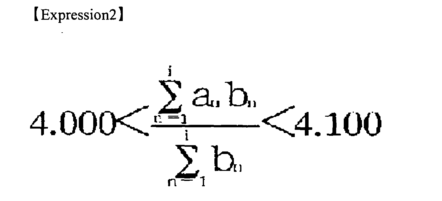
- the B site component may further contain Ti, Zr, and ions other than Ti and Zr; with the piezoelectric ceramic powdered raw material generated by controlling the average valence of the B site component so as to satisfy
- the average valence of the B site component is greater than quadrivalent which is the stoichiometric composition, but less than 4.100, so the A site loss can be formed more effectively with no loss in sinterability, and the A site loss compensates for the dispersion of Ag and the oxygen pores generated by sintering in the low-oxygen atmosphere, whereby reduction in the piezoelectric d constant and deterioration of the insulation resistance can be suppressed even more effectively.
- the molar quantity of Pb included in the A site component may be reduced by 0.5 mol% to 5.0 mol% from that of the stoichiometric composition.
- the pores are formed at the Pb position of the crystal structure (hereafter, these pores will be referred to as "Pb pores”) by reducing the molar quantity of Pb by a predetermined amount, and the Pb pores compensate for the oxygen pores generated by sintering in the low-oxygen atmosphere and dispersion of the internal electrode material, whereby reduction in the piezoelectric d constant can be suppressed.
- the B site component may also contain Nb, and the B site component may contain also Nb and Ni.
- the B site component may also contain at least one or more components selected from Nb, Sb, Ta and W, and the B site component may also contain at least one or more components selected from Ni, Cr, Co and Mg.
- the layered article fabrication step may comprise a ceramic green sheet fabrication step for forming the piezoelectric ceramic powdered raw material into a sheet form so as to fabricate a ceramic green sheet, a step for forming an electrode pattern on the ceramic green sheet with an electroconductive paste for internal electrodes, and a step for layering the ceramic green sheets upon which the electrode patterns have been formed so as to form a layered article.
- the electroconductive paste may contain Ag as a primary component.
- the monolithic piezoelectric part according to the present invention may be manufactured by the above-described method.
- Fig. 1 is a cross-sectional diagram illustrating an embodiment (first embodiment) of a monolithic piezoelectric actuator serving as a monolithic piezoelectric part, manufactured by the manufacturing method according to the present invention.
- the monolithic piezoelectric actuator is configured of a monolithic piezoelectric device, comprises a piezoelectric ceramic body 1 of which the primary component is lead zirconate titanate (Pb (Zi, Ti) O 3 ; PZT) as the perovskite compound oxide expressed by the general formula of ABO 3 , external electrodes 2 (2a, 2b) made of Ag or the like and formed with an L-shaped cross-sectional shape over the top and bottom face to the sides of the piezoelectric ceramic body 1, and internal electrodes 3 (3a through 3f) embedded within the piezoelectric ceramic body 1 in a parallel-opposed array.
- the primary component is lead zirconate titanate (Pb (Zi, Ti) O 3 ; PZT) as the perovskite compound oxide expressed by the general formula of ABO 3
- external electrodes 2 (2a, 2b) made of Ag or the like and formed with an L-shaped cross-sectional shape over the top and bottom face to the sides of the piezoelectric ceramic body
- one end of the internal electrodes 3a, 3c, and 3e are electrically connected to one of the external electrodes, external electrode 2b, and one end of the internal electrodes 3b, 3d, and 3f are electrically connected to the other external electrode 2a.
- the direction of polarization of the monolithic piezoelectric actuator is perpendicular to the face of the internal electrodes 3, with each layer alternately polarized in the opposite direction. Then, by application of voltage between the external electrode 2a and 2b, the monolithic piezoelectric actuator is displaced in the longitudinal direction indicated by the arrow A due to piezoelectric transversal effects.
- the internal electrodes 3 are formed of a mixture of Ad and Pg, prepared so that the ratio by weight of Ag to Pd is 70/30 to 95/5.
- the content of Ag is preferably prepared to be 80 wt% or greater from the perspective of increasing the inclusion amount of less expensive Ag to reduce costs, and the content of Ag is more preferably prepared to be 85 wt% or greater.
- a pulverizing medium therein such as a zirconia ball or the like
- the mixed powder is subjected to calcination at 800°C to 1000°C, thereby making a PZT ceramic powder raw material of which the primary component is represented by the chemical formula of PB 0.950 ⁇ 0.995 (Zr, Ti) O 3 , i.e., a piezoelectric ceramic powdered raw material (hereafter, referred to simply as "ceramic powder raw material") wherein the molar quantity of Pb is reduced by 0.5 mol% to 5.0 mol% from that of the stoichiometric composition.
- a piezoelectric ceramic powdered raw material hereafter, referred to simply as "ceramic powder raw material
- the piezoelectric ceramic body 1 is formed by sintering a layered article formed of multiple piezoelectric ceramic layers and internal electrode layers introduced between the piezoelectric ceramic layers, and in the event that the thickness of each of the piezoelectric ceramic layers is reduced or the percentage of Ag contained as the electrode material which is the primary component of the internal electrode layers is increased, the amount of dispersion of Ag into the piezoelectric ceramic body 1 increases, which promotes formation of oxygen pores, to bring about reduction in the piezoelectric d constant.
- the molar quantity of Pb contained is reduced by 0.5 mol% to 5.0 mol% from that of the stoichiometric composition.
- ceramic sheets (hereafter, referred to simply as "ceramic sheets") are fabricated by the doctor blade method.
- the ceramic sheets which are formed 18 to 130 ⁇ m thick, are preferably made to be as thin as possible in order to allow application of high field emission with a constant application voltage and to obtain great displacement, and 64 ⁇ m or less (40 ⁇ m or less in the thickness after sintering) is preferable from the perspective of obtaining a small and/or high-performance monolithic piezoelectric actuator.
- screen printing is performed on the ceramic sheets with an electroconductive paste for internal electrodes prepared such that the ratio by weight of Ag as to Pd is 70/30 to 95/5 (preferably 80/20 or higher, and even more preferably 85/15 or higher).
- a predetermined number of the ceramic sheets upon which screen printing has been performed are layered, then sandwiched between ceramic sheets upon which screen printing has not been preformed, and compressed, so as to form a layered article. That is, a layered article is fabricated with internal electrode layers disposed between multiple piezoelectric ceramic layers.
- the layered article is stored in an alumina case, subjected to degreasing, and then subjected to sintering processing at a sintering temperature of 950°C to 1080°C for 4 to 32 hours, with the oxygen concentration set to 5 vol% or less but more than 0 vol%.
- the reason that the oxygen concentration has been controlled so as to be 5 vol% or lower is as follows.
- the molar quantity of Pb contained is reduced by 0.5 mol% to 5.0 mol% from that of the stoichiometric composition, so that Pb pores formed thereby compensate for the oxygen pore generation reaction, and decrease in the piezoelectric d constant can be avoided even in a low-oxygen atmosphere.
- the piezoelectric d constant deteriorates and grain growth occurs which aggravates the density of the sintered article in the event that the layers are made thinner or in the event that the percentage of Ag contained in the internal electrode material is increased, which can lead to deterioration in insulation reliability and in strength.
- the oxygen concentration is controlled at 5 vol% or less but more than 0 vol%, and preferably at 0.01 vol% or more but 1.0 vol% or less, for sintering.
- the piezoelectric ceramic body 1 has electroconductive paste for external electrodes applied on predetermined positions on the surface thereof, and sintered, so as to form the external electrodes 3, whereby the monolithic piezoelectric actuator is formed.
- a ceramic powder raw material wherein the primary component thereof is represented by the chemical formula of PB 0.950 ⁇ 0.995 (Zr, Ti) O 3 is generated by reducing the molar quantity of Pb contained by 0.5 mol% to 5.0 mol% from that of the stoichiometric composition, and by forming the piezoelectric ceramic body 1 with this ceramic powder raw material Pb pores can be formed.
- the Pb pores compensate for the dispersion of Ag and for the oxygen pores generated by sintering in the low-oxygen atmosphere, which suppresses decrease in the piezoelectric d constant and deterioration in insulation resistance, so a highly reliable monolithic piezoelectric actuator with excellent piezoelectric properties can be manufactured.
- Nb 5+ , Sb 5+ , Ta 5+ and W 6+ which have a greater valence than Ti 4+ or Zr 4+
- part of the Zr for example is substituted with the donor ions to have a donor excess effect, which results in formation of Pb pores, and the Pb pores compensate for the dispersion of Ag and the oxygen pores generated by sintering in the low-oxygen atmosphere, and thereby decrease in the piezoelectric d constant and deterioration in insulation resistance can be suppressed even more effectively.
- the effects are even greater when Nb 5+ is included as a donor ion, in particular.
- the reason that the average valence of the B site component has been set to 4.100 or less in the above Expression is that the sinterability deteriorates when the average valence is 4.100 or greater, and in the process of co-sintering with internal electrode materials containing a high percentage of Ag, insufficient sintering or deformation of the sintered article may occur at sintering temperatures where normal co-sintering can be performed.
- the average valence of the B site component can be controlled by measuring a predetermined molar amount of the ions contained, in the form of metal oxides, along with the above-described ceramic raw material.
- a predetermined molar quantity of one or more selected from together with Pb 3 O 4 , ZrO 2 , and TiO 2 , Nb 2 O 5 , Sb 2 O 5 , Ta 2 O 5 , WO 3 (preferably including Nb 2 O 5 ) and, if necessary, one or more selected from NiO, CoO, MgO, and Cr 2 O 3 , (preferably including NiO) is measured so as to set the average valence of the B site component to a predetermined value of quadrivalent or greater (but less than 4.100), and then by the same method and procedures as described above a monolithic piezoelectric actuator wherein donor excess has been effected can be readily manufactured.
- the present invention is not restricted to the above-described embodiment. While the above embodiment has been described with reference to an example of a monolithic piezoelectric actuator as the monolithic piezoelectric part, it is needless to say that this may be applied in the same manner to other monolithic piezoelectric parts such as piezoelectric audio emitters, piezoelectric sensors, and so forth, which require a high piezoelectric d constant, neither the layered structure, device shape, direction of displacement and force, polarization direction, and voltage application direction are restricted to the above embodiment.
- Fig. 2 is a cross-sectional diagram illustrating a monolithic piezoelectric audio emitter as a second embodiment of the monolithic piezoelectric part.
- the monolithic piezoelectric audio emitter has a monolithic piezoelectric device 4 and a diaphragm 5 bonded one to another. Also, the monolithic piezoelectric device 4 has external electrodes 7a and 7b formed on the surface of the piezoelectric ceramic body 6 of which PZT is the primary component, and further, internal electrodes 6a through 6c are embedded within the piezoelectric ceramic body 6 in a parallel-opposed array.
- the monolithic piezoelectric device 4 has one end of the internal electrodes 6a and 6c electrically connected to one of the external electrodes, external electrode 7b, and one end of the internal electrode 6b is electrically connected to the other external electrode 7a.
- the monolithic piezoelectric device 4 is displaced in the longitudinal direction indicated by the arrow B due to piezoelectric transversal effects, and this displacement causes excitation of flexion vibrations at the diaphragm 5, to emit sound.
- manufacturing the piezoelectric ceramic body 6 by the above-described manufacturing method allows decrease in the piezoelectric d constant and deterioration in insulation resistance to be effectively suppressed, so a monolithic piezoelectric audio emitter with excellent reliability is manufactured.
- Fig. 3 is a cross-sectional diagram illustrating a monolithic piezoelectric sensor as a third embodiment of the monolithic piezoelectric part.
- the monolithic piezoelectric sensor is made up of the monolithic piezoelectric device and has external electrodes 10a and 10b formed on the surface of a piezoelectric ceramic body 9 of which PZT is the primary component, and further, internal electrodes 11a through 11e are embedded within the piezoelectric ceramic body 9 in a parallel-opposed array.
- the monolithic piezoelectric sensor has one end of the internal electrodes 1 1a, 11c, and 11e electrically connected to one of the external electrodes, external electrode 10b, and one end of the internal electrodes 11b and 11d electrically connected to the other external electrode 10a.
- Application of force in the direction indicated by the arrow C generates a charge between the external electrode 10a and the external electrode 10b due to piezoelectric longitudinal effects, and force is detected by this charge.
- manufacturing the piezoelectric ceramic body 9 by the above-described manufacturing method allows decrease in the piezoelectric d constant and deterioration in insulation resistance to be effectively suppressed, so a monolithic piezoelectric sensor with excellent reliability can be manufactured.
- the process for forming the layered article is not restricted to the sheet method. It is needless to say that similar effects can be obtained by using other layered article formation processes, such as print-laminating process or the like, for example.
- the inventors prepared test pieces of monolithic piezoelectric parts with different composition ratios of ceramic powder raw materials (Examples 1 through 18 and Comparative examples 1 through 9), and evaluated the amount of Ag dispersion, piezoelectric d 31 constant, and insulation resistance.
- Pb 3 O 4 , TiO 2 , and ZrO 2 were prepared as ceramic raw material, and Pb 3 O 4 was measured such that the molar quantity of Pb contained making up the A site would be less than that of the stoichiometric composition by 0.5 mol% to 5.0 mol%, while TiO 2 and ZrO 2 were measured such that the molar quantity contained in Ti and Zr making up the B site would be 44.5 to 45.5 mol% and 54.5 to 55.5 mol%, respectively.
- the measured materials were placed in a ball mill with a zirconia ball therein as a pulverizing medium, mixed and pulverized for 16 to 64 hours, and then the obtained mixed powder was subjected to calcination at 800°C to 1000°C, to make a ceramic powder raw material.
- the ceramic sintered article was diced into 3 mm vertically and 13 mm horizontally, and external electrodes were formed with the electroconductive paste for external electrodes, and then polarization processing was performed for 5 to 30 minutes in an insulating oil at 40 to 80°C with an electric field of 2 to 3 kV applied, to fabricate the test pieces for the Examples 1 through 3.
- Pb 3 O 4 , TiO 2 , ZrO 2 , and Nb 2 O 5 were prepared as ceramic raw material, and Pb 3 O 4 was measured such that the molar quantity of Pb contained would be less than that of the stoichiometric composition by 0.5 mol% to 5.0 mol%, and TiO 2 , ZrO 2 and Nb 2 O 5 were measured such that the molar quantity of Ti, Zr, and Nb contained making up the B site would be 44.0 to 45.0 mol%, 54.0 to 55.0 mol%, and 1.0 mol%, respectively, then they were subjected to wet mixing pulverization, and to calcination, to make a ceramic powder raw material with an average valence of the B site at 4.010.
- test pieces for Examples 4 through 7 were fabricated by the same method and procedures as for the above Examples 1 through 3.
- Pb 3 O 4 , TiO 2 , ZrO 2 , Nb 2 O 5 and NiO were prepared as ceramic raw material, and Pb 3 O 4 was measured such that the molar quantity of Pb contained would be less than that of the stoichiometric composition by 0.5 mol% to 5.0 mol%, and TiO 2 , ZrO 2 Nb 2 O 5 , and NiO were measured such that the molar quantity of Ti, Zr, Nb, and Ni contained making up the B site would be 38.0 to 39.0 mol%, 35.5 to 36.5 mol%, 17.0 to 17.3 mol%, and 8.2 to 8.5 mol%, respectively, then they were subjected to wet mixing pulverization, and to calcination, to make a ceramic powder raw material with an average valence of the B site between 4.000 and 4.009.
- ceramic sheets were fabricated with the same method and procedures as for the above Examples 1 through 3, screen printing was performed on the ceramic sheets with an electroconductive paste for internal electrodes prepared such that the ratio by weight of Ag to Pd was 90/10, to form a layered article.
- the layered article was stored in an alumina case, subjected to degreasing, and then to sintering processing at a sintering temperature of 980°C for 4 to 32 hours, with the oxygen concentration set to 0.2 vol%, thereby a ceramic sintered article was fabricated.
- test pieces for Examples 8 through 14 were fabricated by the same method and procedures as for the above Examples 1 through 3.
- Pb 3 O 4 TiO 2 , ZrO 2 , Nb 2 O 5 , NiO, Sb 2 O 5 , Ta 2 O 5 , WO 3 , Cr 2 O 3 , CoO and MgO were prepared as ceramic raw material, Pb 3 O 4 was measured such that the molar quantity of Pb contained would be less than that of the stoichiometric composition by 0.5 to 1.5 mol%, and TiO 2 , ZrO 2 , Nb 2 O 5 , NiO, Sb 2 O 5 , Ta 2 O 5 , WO 3 , Cr 2 O 3 , CoO, and MgO were measured such that the molar quantity of Ti, Zr, Nb, Ni, Sb, Ta, W, Cr, Co, and Mg contained making up the B site would be 34.0 to 39.0 mol%, 16.0 to 35.5 mol%, 13.0 to 35.0 mol%, 6.0 to 15.0 mol%, 0 to 3.3 mol%, 0 to 0.5 mol
- ceramic sheets were fabricated by the same method and procedures as in the above Examples 1 through 3, screen printing was performed on the ceramic sheets with an electroconductive paste for internal electrodes prepared such that the ratio by weight of Ag to Pd was 80/20 to 85/15, to form a layered article.
- the layered article was stored in an alumina case, subjected to degreasing, and then to sintering processing at a sintering temperature of 1020 to 1040°C for 4 to 32 hours, with the oxygen concentration set to 0.2 vol%, to fabricate a ceramic sintered article.
- test pieces for Examples 15 through 18 were fabricated by the same method and procedures as in the above Examples 1 through 3.
- Test pieces for Comparative examples 1 and 2 were fabricated by the same method and procedures as in Examples 1 through 3, except that the molar quantity of Pb contained was the same as that of the stoichiometric composition or less than that of the stoichiometric composition by 8 mol%.
- Test pieces for the Comparative examples 3 and 4 were fabricated with the same method and procedures as for the Examples 4 through 7, except that the molar quantity of Pb contained was the same as that of the stoichiometric composition or less than that of the stoichiometric composition by 8 mol%.
- Test pieces for Comparative examples 5 through 8 were fabricated by the same method and procedures as in Examples 8 through 14, except that the molar quantity of Pb contained was the same as that of the stoichiometric composition or less than that of the stoichiometric composition by 8 mol%.
- a test piece for Comparative example 9 was fabricated by the same method and procedures as in Examples 15 through 18, except that the molar quantity of Pb contained was that of the stoichiometric composition, and the amount of Nb and Ni contained was 36.7 mol% and 13.3 mol% respectively, and the average valence of the B site was set to 4.101.
- the inventors measured the amount of Ag dispersed into the ceramic body, the piezoelectric d 31 constant, and the resistivity log ⁇ for each test piece.
- Measurement of the dispersion amount of Ag was performed by quantitative analysis by an X-ray micro-analyzer (Wave Dispersive X-ray; hereafter referred to as "WDX") Measurement of the amount of Ag contained in the analysis region was performed by an analytical curve created by use of a sample where the amount of Ag contained is known.
- WDX Wide Dispersive X-ray
- the piezoelectric d 31 constant was measured by the resonance-antiresonance method, with an impedance analyzer (Model HP4194, manufactured by Hewlett-Packard Company).
- the resistivity log ⁇ was calculated by measurement of the insulation resistance by applying a DC electric field of 100 to 300 V/mm for 30 seconds to 1 minute at a temperature of 25°C, with an Ultra-High Resistance/Micro Current Meter (Model R8240A, manufactured by Advantest Corporation),.
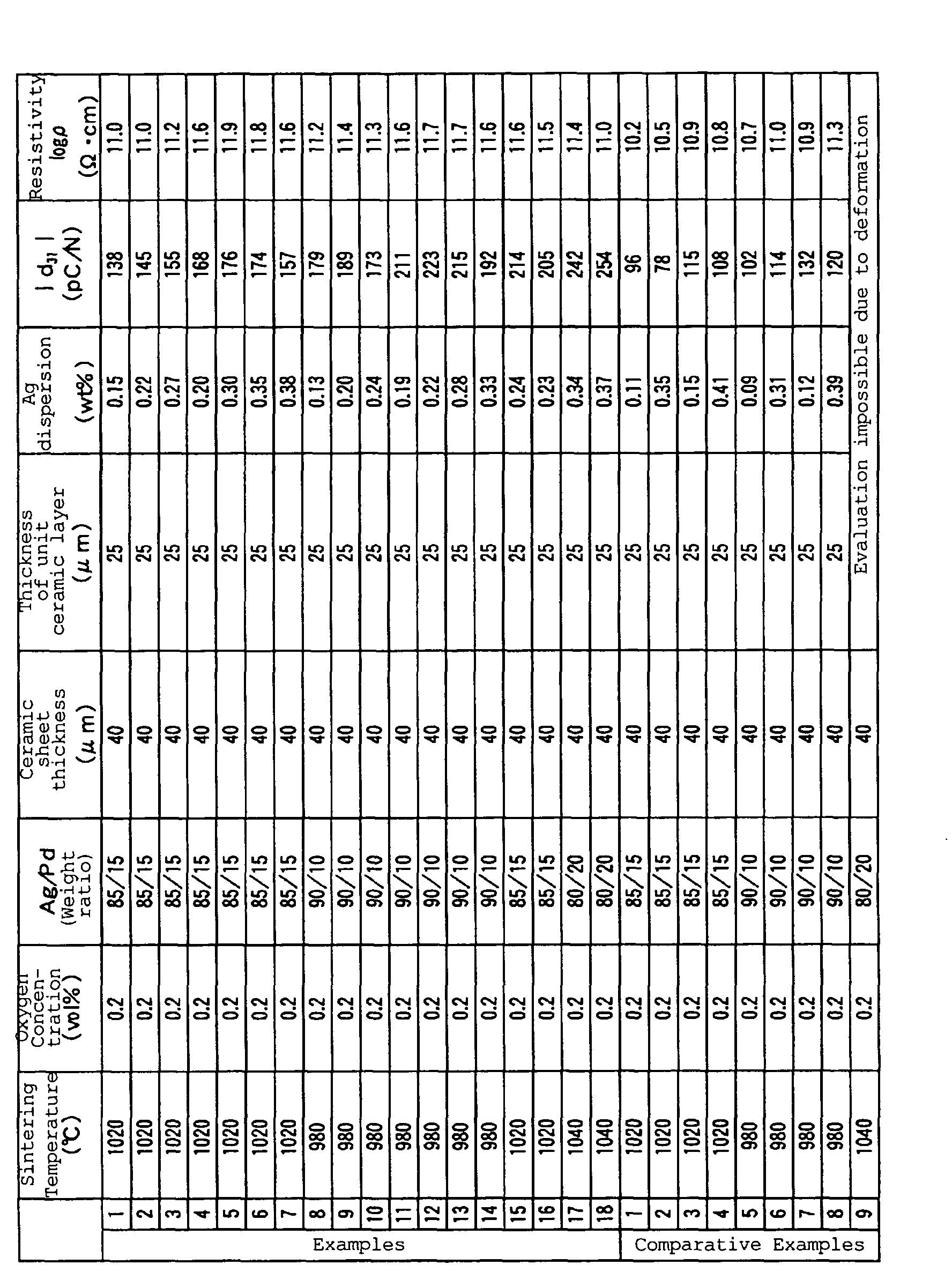
- Table 1 illustrates the component compositions of the Examples 1 through 18 and Comparative examples 1 through 9, and Table 2 illustrates the sintering temperature, oxygen concentration in the atmosphere at the time of sintering, the ratio by weight of Ag to Pd which are the internal electrode material, the thickness of the ceramic sheets, the thickness of each unit ceramic layer after sintering, and the results of the above measurement.
- the average value was calculated through observation of the cross-sectional surface of the ceramic sintered article after sintering with an optical microscope.
- the average valence of the B site was 4.101, meaning a donor excess, and/or the molar quantity of Pb contained is the same as that of the stoichiometric composition (100 mol%), so deformation after sintering was serious and sintering was insufficient to the extent that its evaluation was impossible.
- the inventors fabricated test pieces of the monolithic piezoelectric part in the same way as with the first embodiment using the ceramic powder raw material of the same composition as with Example 12 and Comparative example 5, changing the oxygen concentration of the sintering atmosphere in various ways.
- Ceramic sheets were fabricated with the same method and procedures as in the first embodiment with the ceramic powder raw material of the same composition as in Example 12, and screen printing was performed on the ceramic sheets with an electroconductive paste for internal electrodes prepared such that the ratio by weight of Ag to Pd was 90/10, and then a layered article was formed.
- the layered article was stored in an alumina case, subjected to degreasing, and then subjected to sintering processing at a sintering temperature of 980°C for 4 to 32 hours, with the oxygen concentration set to 0.01 to 5.0 vol%, and thereby a ceramic sintered article was fabricated.
- test pieces for Examples 21 through 25 were fabricated by the same method and procedures as in the first embodiment.
- Test pieces for Comparative examples 21 and 22 were fabricated with the ceramic powder raw material of the same composition as in Examples 21 through 25, by sintering with the oxygen concentration at 10.0 vol% and 21.0 vol%, respectively.
- Ceramic sheets were fabricated by the same method and procedures as in the first embodiment with the ceramic powder raw material of the same composition as in Comparative example 5, and screen printing was performed on the ceramic sheets with an electroconductive paste for internal electrodes prepared so that the ratio by weight of Ag to Pd was 90/10, to form a layered article.
- the layered article was stored in an alumina case, subjected to degreasing, and then test pieces for Comparative examples 23 through 28 were fabricated by the same method and procedures as in Examples 21 through 24, with the oxygen concentration set to 0.05 to 21.0 vol%.
- the inventors measured, as in the first embodiment, the amount of Ag dispersion into the ceramic body, the piezoelectric d 31 constant, and the resistivity log ⁇ , for each test piece. Further, the average grain diameter was calculated by the intercept method through observation of the cross-sectional surface of the ceramic sintered article after sintering with a scanning electron microscope.
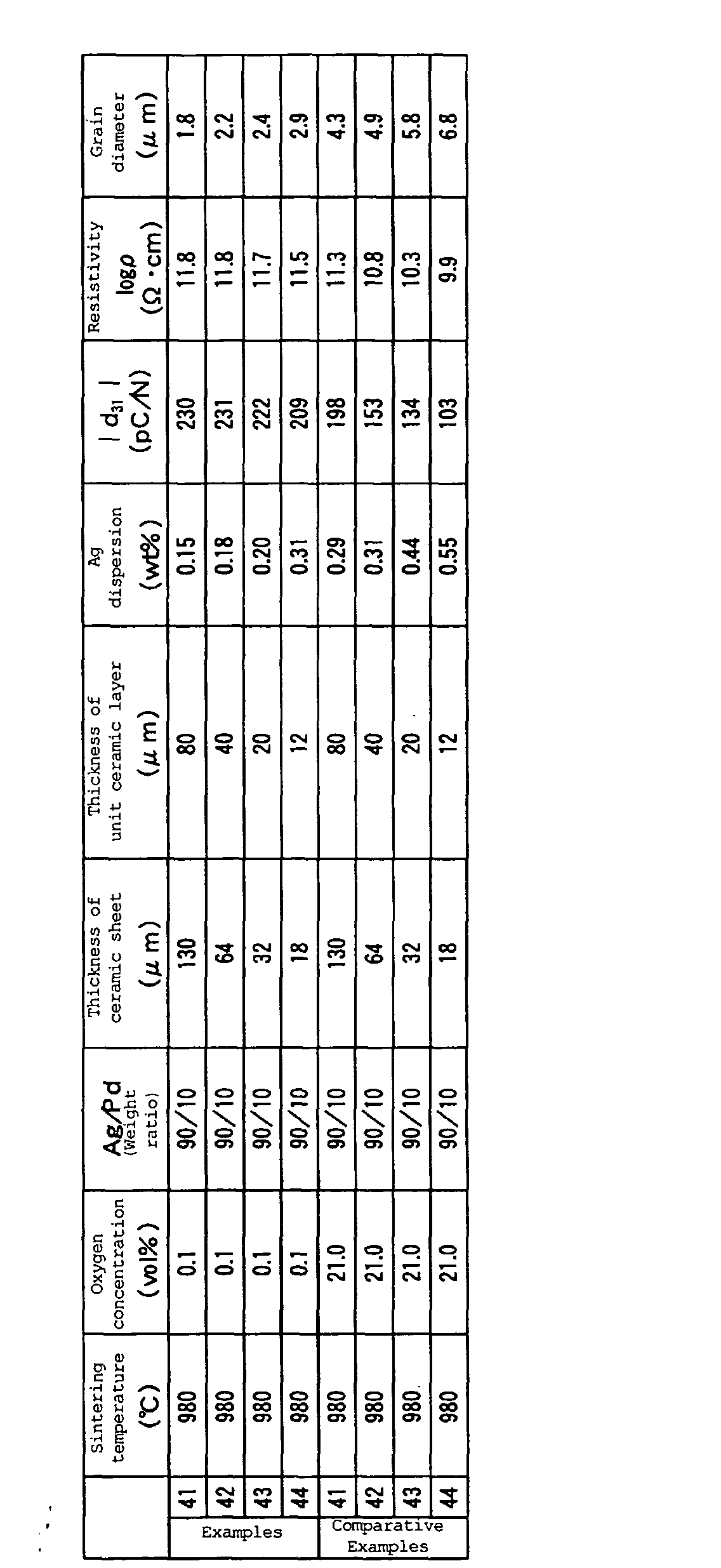
- Table 3 illustrates the sintering temperature, oxygen concentration in the atmosphere at the time of sintering, the ratio by weight Ag/Pd of the internal electrodes, the thickness of the ceramic sheets, the thickness of each unit ceramic layer after sintering, and the results of the above measurement, in Examples 21 through 25 and Comparative examples 21 through 28.
- Comparative examples 23 through 26 the molar quantity of Pb contained is the same as that of the stoichiometric composition, and moreover, sintering is performed within a low-oxygen atmosphere, so generation of oxygen pores is promoted, and decrease in piezoelectric d 31 constant was observed.
- Comparative examples 27 and 28 the oxygen concentration is high at 10.0 vol% and 21.0 vol%, respectively, so grain growth was observed as in Comparative examples 21 and 22, and decrease in insulation resistance was confirmed by the result that the resistivity log ⁇ was less than 11.0 ⁇ cm.
- the inventors fabricated test pieces of the monolithic piezoelectric part in the same way as in the first embodiment with the ceramic powder raw material of the same composition as in Example 12 and Comparative example 5, by changing the Ag/Pd weight ratio of the internal electrodes in various ways.
- Ceramic sheets with a thickness of 32 ⁇ m were fabricated, as in the second embodiment, with the ceramic powder raw material of the same composition as in Example 12, and screen printing was performed on the ceramic sheets with an electroconductive paste for internal electrodes prepared so that the ratio by weight of Ag to Pd was 95/5 to 70/30, to form a layered article.
- the layered article was stored in an alumina case, subjected to degreasing, and then to sintering processing at a sintering temperature of 950 to 1080°C for 4 to 32 hours, with the oxygen concentration set to 0.2 vol%, and thereby a ceramic sintered article with a unit ceramic layer thickness following sintering of 20 ⁇ m was fabricated.
- test pieces for Examples 31 through 35 were fabricated in the same way as in the first embodiment.
- Ceramic sheets with a thickness of 32 ⁇ m were fabricated by the same method and procedures as in the second embodiment with the ceramic powder raw material of the same composition as in Comparative example 5, and screen printing was performed on the ceramic sheets with an electroconductive paste for internal electrodes prepared so that the ratio by weight Ag to Pd was 95/5 to 70/30, to form a layered article.
- the layered article was stored in an alumina case, subjected to degreasing, and then to sintering processing at a sintering temperature of 950 to 1080°C for 4 to 32 hours, with the oxygen concentration set to 21.0 vol%, and thereby a ceramic sintered article was fabricated.
- test pieces for Comparative Examples 31 through 35 were fabricated in the same way as in the first embodiment.
- the inventors measured the amount of Ag dispersion into the ceramic body, the piezoelectric d 31 constant, the resistivity log ⁇ , and the grain diameter after sintering.
- Table 4 illustrates the sintering temperature, oxygen concentration in the atmosphere at the time of sintering, the ratio by weight of Ag to Pd, the thickness of the ceramic sheets, the thickness of each unit ceramic layer after sintering, and the results of the above measurement, in Examples 31 through 35 and Comparative examples 31 through 35.
- the inventors fabricated test pieces of the monolithic piezoelectric part in the same way as in the first embodiment with the ceramic powder raw material of the same composition as in Example 12 and Comparative example 5, to fabricate ceramic sheets with different in thickness.
- Ceramic sheets in a thickness of 18 to 130 ⁇ m were fabricated by the same method and procedures as in the second embodiment with the ceramic powder raw material of the same composition as in Example 12, and screen printing was performed on the ceramic sheets with an electroconductive paste for internal electrodes prepared so that the ratio by weight of Ag to Pd was 90/10, to form a layered article, of which the number of layers was between 4 to 30.
- the layered article was stored in an alumina case, and subjected to degreasing and sintering processing at a sintering temperature of 980°C for 4 to 32 hours, with the oxygen concentration set to 0.1 vol%, to fabricate a ceramic sintered article with unit ceramic layers of 12 to 80 ⁇ m after sintering.
- test pieces for Examples 41 through 44 were fabricated in the same way as in the first embodiment.
- Ceramic sheets in a thickness of 18 to 130 ⁇ m were fabricated by the same method and procedures as in the second embodiment with the ceramic powder raw material of the same composition as in Comparative Example 5, and screen printing was performed on the ceramic sheets with an electroconductive paste for internal electrodes prepared so that the ratio by weight of Ag to Pd was 90/10, to form a layered article of which the number of layers was between 4 to 30.
- the layered article was stored in an alumina case, and subjected to degreasing and sintering processing at a sintering temperature of 980°C for 4 to 32 hours, with the oxygen concentration set to 21.0 vol%, to fabricate a ceramic sintered article with unit ceramic layers of 12 to 80 ⁇ m.
- test pieces for Comparative Examples 41 through 44 were fabricated in the same way as in the first embodiment.
- the inventors measured the amount of Ag dispersion into the ceramic body, the piezoelectric d 31 constant, the resistivity log ⁇ , and the grain diameter after sintering.
- Table 5 illustrates the sintering temperature, oxygen concentration in the atmosphere at the time of sintering, the ratio by weight of Ag to Pd, the thickness of the ceramic sheets, the thickness of each unit ceramic layer after sintering, and the results of the above measurement, in Examples 41 through 44 and Comparative examples 41 through 44.
- Examples 41 through 44 it was confirmed that a high piezoelectric d 31 constant of 209 to 230 pC/N could be obtained, without dependence on the thickness of the unit ceramic layer (or thickness of the ceramic sheet).
- the thickness of the unit ceramic layer was 40 ⁇ m or less (or the thickness of the ceramic sheet was 64 ⁇ m or less)
- the piezoelectric d 31 constant and the insulation resistance was markedly improved in comparison with Comparative examples 42 through 44 wherein the thickness of the unit ceramic layer (or thickness of the ceramic sheet) was the same as in the above examples.
Landscapes
- Engineering & Computer Science (AREA)
- Chemical & Material Sciences (AREA)
- Manufacturing & Machinery (AREA)
- Ceramic Engineering (AREA)
- Composite Materials (AREA)
- Materials Engineering (AREA)
- Structural Engineering (AREA)
- Organic Chemistry (AREA)
- Compositions Of Oxide Ceramics (AREA)
- Piezo-Electric Transducers For Audible Bands (AREA)
- Piezo-Electric Or Mechanical Vibrators, Or Delay Or Filter Circuits (AREA)
Abstract
Description




Claims (11)
- A method for manufacturing a monolithic piezoelectric part which has a plurality of piezoelectric ceramic layers and internal electrode layers disposed with said piezoelectric ceramic layers introduced therebetween, wherein said piezoelectric ceramic making up said piezoelectric ceramic layers is formed of a perovskite compound oxide expressed by the general formula of ABO3, and contains at least Pb for the A site component and at least Ti for the B site component; said method comprises:a powdered raw material generation step for generating a piezoelectric ceramic powdered raw material wherein the molar quantity of said A site component has been reduced by 0.5 mol% to 5.0 mol% from that of the stoichiometric composition;a layered article fabrication step for fabricating a layered article with said piezoelectric ceramic powdered raw material; anda sintering step for subjecting said layered article to sintering processing within an atmosphere wherein the oxygen concentration is 5% by volume or less but more than 0% by volume.
- A method for manufacturing a monolithic piezoelectric part according to Claim 1, wherein, in said powdered raw material generating step, the ceramic raw material making up said A site component and the ceramic raw material making up said B site component are combined so that the average valence of said B site component is greater than that of the stoichiometric composition.
- A method for manufacturing a monolithic piezoelectric part according to Claim 2, wherein said B site component further contains Ti, Zr, and ions other than Ti and Zr;
and wherein said piezoelectric ceramic powdered raw material is generated by controlling the average valence of said B site component so as to satisfy Expression 1wherein the valence of ions Mn (n = 1, 2, 3, ..., i) included in said B site component is represented as an (n = 1, 2, 3, ..., i), and the molar ratio of said Mn is represented as bn (n = 1, 2, 3, ..., i).
- A method for manufacturing a monolithic piezoelectric part according to any of the Claims 1 through 3, wherein, in said powdered raw material generation step, the molar quantity of Pb included in said A site component has been reduced by 0.5 mol% to 5.0 mol% from that of the stoichiometric composition.
- A method for manufacturing a monolithic piezoelectric part according to any of the Claims 1 through 4, wherein said B site component further contains Nb.
- A method for manufacturing a monolithic piezoelectric part according to any of the Claims 1 through 4, wherein said B site component further contains Nb and Ni.
- A method for manufacturing a monolithic piezoelectric part according to any of the Claims 1 through 4, wherein said B site component further contains at least one or more components selected from Nb, Sb, Ta and W.
- A method for manufacturing a monolithic piezoelectric part according to Claim 7, wherein said B site component further contains at least one or more components selected from Ni, Cr, Co and Mg.
- A method for manufacturing a monolithic piezoelectric part according to any of the Claims 1 through 8, wherein said layered article fabrication step comprises a ceramic green sheet fabrication step for forming said piezoelectric ceramic powdered raw material into a sheet form so as to fabricate a ceramic green sheet, a step for forming an electrode pattern on said ceramic green sheet with an electroconductive paste for internal electrodes, and a step for layering ceramic green sheets upon which said electrode patterns have been formed so as to form a layered article.
- A method for manufacturing a monolithic piezoelectric part according to any of the Claims 1 through 9, wherein said electroconductive paste contains Ag as a primary component.
- A monolithic piezoelectric part, manufactured by a method according to any of the Claims 1 through 10.
Applications Claiming Priority (4)
| Application Number | Priority Date | Filing Date | Title |
|---|---|---|---|
| JP2002216120 | 2002-07-25 | ||
| JP2002216120 | 2002-07-25 | ||
| JP2003002988 | 2003-01-09 | ||
| JP2003002988A JP3678234B2 (en) | 2002-07-25 | 2003-01-09 | Method for manufacturing multilayer piezoelectric component and multilayer electronic component |
Publications (3)
| Publication Number | Publication Date |
|---|---|
| EP1387417A2 true EP1387417A2 (en) | 2004-02-04 |
| EP1387417A3 EP1387417A3 (en) | 2006-02-15 |
| EP1387417B1 EP1387417B1 (en) | 2007-02-07 |
Family
ID=30117486
Family Applications (1)
| Application Number | Title | Priority Date | Filing Date |
|---|---|---|---|
| EP20030016741 Expired - Lifetime EP1387417B1 (en) | 2002-07-25 | 2003-07-22 | Manufacturing method for monolithic piezoelectric part |
Country Status (8)
| Country | Link |
|---|---|
| US (1) | US7431785B2 (en) |
| EP (1) | EP1387417B1 (en) |
| JP (1) | JP3678234B2 (en) |
| KR (1) | KR100553226B1 (en) |
| CN (1) | CN100382352C (en) |
| AT (1) | ATE353477T1 (en) |
| DE (1) | DE60311613T2 (en) |
| TW (1) | TWI226714B (en) |
Cited By (1)
| Publication number | Priority date | Publication date | Assignee | Title |
|---|---|---|---|---|
| WO2005051862A1 (en) | 2003-11-26 | 2005-06-09 | Kyocera Corporation | Piezoelectric ceramic and laminated piezoelectric device |
Families Citing this family (30)
| Publication number | Priority date | Publication date | Assignee | Title |
|---|---|---|---|---|
| WO2005029602A1 (en) * | 2003-09-24 | 2005-03-31 | Kyocera Corporation | Multilayer piezoelectric device |
| CN100587989C (en) * | 2004-06-24 | 2010-02-03 | 京瓷株式会社 | Multilayer electronic component and ejection device using the same |
| JP4925825B2 (en) * | 2004-06-24 | 2012-05-09 | 京セラ株式会社 | Multilayer electronic component and injection device using the same |
| JP4997521B2 (en) * | 2004-11-15 | 2012-08-08 | 独立行政法人物質・材料研究機構 | Piezoelectric materials and nonlinear piezoelectric elements |
| JP4873327B2 (en) * | 2005-06-03 | 2012-02-08 | 株式会社村田製作所 | Piezoelectric element |
| KR100700349B1 (en) * | 2005-09-15 | 2007-03-29 | 재단법인서울대학교산학협력재단 | Multilayer Type 1-3 Piezo-Composite Ultrasonic Transducer Using Transverse Mode |
| JP2007314368A (en) * | 2006-05-25 | 2007-12-06 | Fujifilm Corp | Perovskite oxide, ferroelectric element, piezoelectric actuator, and liquid ejection device |
| KR100846052B1 (en) * | 2006-06-26 | 2008-07-11 | 재단법인서울대학교산학협력재단 | 2-2 Piezoelectric Composite Ultrasonic Oscillator and Manufacturing Method |
| WO2008068975A1 (en) * | 2006-12-06 | 2008-06-12 | Murata Manufacturing Co., Ltd. | Laminated piezoelectric device and process for manufacturing the same |
| JP5305263B2 (en) * | 2007-10-17 | 2013-10-02 | 独立行政法人産業技術総合研究所 | Piezoelectric material for power generation |
| CN101903308B (en) * | 2007-10-18 | 2017-04-19 | 陶瓷技术有限责任公司 | Piezoceramic multi-layer element |
| JP2010150126A (en) * | 2008-11-18 | 2010-07-08 | Ngk Insulators Ltd | Piezoelectric/electrostrictive ceramic composition, piezoelectric/electro-stric sintered compact, piezoelectric/electrostrictive element, method for producing piezoelectric/electrostrictive composition, and method for producing piezoelectric/electrostrictive element |
| JP2010245088A (en) * | 2009-04-01 | 2010-10-28 | Murata Mfg Co Ltd | Method for manufacturing multilayer ceramic electronic component |
| JP5859182B2 (en) * | 2009-08-28 | 2016-02-10 | 株式会社タムラ製作所 | Piezoelectric module |
| KR101109223B1 (en) * | 2010-01-20 | 2012-01-30 | 삼성전기주식회사 | Piezo Actuator |
| KR101009217B1 (en) * | 2010-02-23 | 2011-01-19 | 양병남 | Supporter device for floor |
| US9360938B2 (en) * | 2011-04-26 | 2016-06-07 | Blackberry Limited | Input device with tactile feedback |
| JP2013055085A (en) * | 2011-08-31 | 2013-03-21 | Seiko Epson Corp | Liquid injection head manufacturing method, liquid injection head, piezoelectric element manufacturing method and piezoelectric element |
| US10011103B2 (en) | 2012-03-30 | 2018-07-03 | Nec Corporation | Sheet-laminating device and sheet-laminating method |
| TW201434789A (en) * | 2013-01-29 | 2014-09-16 | Canon Kk | Piezoelectric material, piezoelectric element, and electronic equipment |
| EP2946419B1 (en) * | 2013-01-29 | 2017-11-08 | Canon Kabushiki Kaisha | Piezoelectric material, piezoelectric element, and electronic equipment |
| JP6106009B2 (en) * | 2013-04-03 | 2017-03-29 | 太陽誘電株式会社 | Ceramic electronic components |
| JP5679010B2 (en) * | 2013-05-07 | 2015-03-04 | Tdk株式会社 | Piezoelectric element and manufacturing method thereof |
| EP3099649B1 (en) * | 2014-01-29 | 2018-07-25 | Canon Kabushiki Kaisha | Piezoelectric ceramic, method for producing the same, piezoelectric element, multilayer piezoelectric element, liquid ejection head, liquid ejecting apparatus, ultrasonic motor, optical device, vibrating apparatus, dust-removing apparatus, imaging apparatus, and electronic device |
| KR101630606B1 (en) * | 2014-11-07 | 2016-06-15 | 포항공과대학교 산학협력단 | Manufacturing Method of Piezoelectric element using powder injection molding with Implantable electrode and Piezoelectric element |
| JP2016213410A (en) * | 2015-05-13 | 2016-12-15 | 日立金属株式会社 | Circuit board and method for manufacturing the same |
| DE112017005909T5 (en) * | 2016-11-22 | 2019-09-05 | Kansai University | PIEZOELECTRIC LAMINATE ELEMENT AND LOAD SENSOR, AND A POWER SUPPLY FOR THE USE THEREOF |
| JP7056669B2 (en) * | 2017-11-09 | 2022-04-19 | 株式会社村田製作所 | Piezoelectric components, sensors and actuators |
| JP7426875B2 (en) * | 2020-03-27 | 2024-02-02 | 太陽誘電株式会社 | Piezoelectric element and its manufacturing method |
| CN114773057B (en) * | 2022-05-25 | 2023-05-02 | 国网智能电网研究院有限公司 | Piezoelectric ceramic and contact ultrasonic sensor for partial discharge detection of transformer |
Family Cites Families (25)
| Publication number | Priority date | Publication date | Assignee | Title |
|---|---|---|---|---|
| JPS5939913B2 (en) * | 1978-08-17 | 1984-09-27 | 株式会社村田製作所 | Method of manufacturing piezoelectric porcelain |
| JPS60103079A (en) | 1983-11-05 | 1985-06-07 | 住友特殊金属株式会社 | Piezoelectric ceramic composition |
| JPH0620014B2 (en) | 1988-10-31 | 1994-03-16 | 太陽誘電株式会社 | Multilayer chip inductor and manufacturing method thereof |
| JP2676620B2 (en) | 1988-10-31 | 1997-11-17 | 太陽誘電 株式会社 | Multilayer ceramic capacitor and manufacturing method thereof |
| JPH02122598A (en) | 1988-10-31 | 1990-05-10 | Taiyo Yuden Co Ltd | Ceramic multilayer wiring board and manufacture thereof |
| JP2633442B2 (en) | 1992-06-19 | 1997-07-23 | 株式会社トミー | Ball toys |
| JP3119101B2 (en) | 1994-11-28 | 2000-12-18 | 株式会社村田製作所 | Piezoelectric ceramic composition |
| JPH10163779A (en) | 1996-12-04 | 1998-06-19 | Ngk Insulators Ltd | Method for manufacturing piezoelectric member |
| JPH11163433A (en) * | 1997-11-27 | 1999-06-18 | Hitachi Metals Ltd | Laminating piezoelectric ceramics vibrator and manufacture thereof |
| JPH11274595A (en) * | 1998-03-23 | 1999-10-08 | Hitachi Metals Ltd | Piezoelectric ceramics, lamination type piezoelectric ceramics vibrator and its manufacture |
| JP3341672B2 (en) * | 1998-04-13 | 2002-11-05 | 株式会社村田製作所 | Method for manufacturing piezoelectric ceramic element |
| JP3385999B2 (en) * | 1999-04-08 | 2003-03-10 | 株式会社村田製作所 | Piezoelectric ceramic composition, piezoelectric buzzer and piezoelectric actuator using the same |
| JP3874229B2 (en) * | 1999-07-02 | 2007-01-31 | Tdk株式会社 | Piezoelectric ceramics and piezoelectric device using the same |
| JP3562402B2 (en) * | 1999-09-29 | 2004-09-08 | 株式会社村田製作所 | Piezoelectric ceramic material and surface wave device using the same |
| US20020098333A1 (en) * | 1999-12-16 | 2002-07-25 | Adalbert Feltz | Piezoceramic device |
| JP4496579B2 (en) * | 1999-12-28 | 2010-07-07 | Tdk株式会社 | Piezoelectric ceramic composition |
| JP4683689B2 (en) * | 2000-03-29 | 2011-05-18 | 京セラ株式会社 | Multilayer piezoelectric element, piezoelectric actuator, and injection device |
| US6653762B2 (en) * | 2000-04-19 | 2003-11-25 | Murata Manufacturing Co., Ltd. | Piezoelectric type electric acoustic converter |
| JP2001302348A (en) | 2000-04-19 | 2001-10-31 | Tokin Corp | Piezoelectric ceramic composition |
| JP3991564B2 (en) * | 2000-08-25 | 2007-10-17 | 株式会社村田製作所 | Piezoelectric ceramic composition and piezoelectric element |
| DE10055241A1 (en) * | 2000-11-08 | 2002-05-29 | Epcos Ag | piezo actuator |
| US6964718B2 (en) * | 2000-11-16 | 2005-11-15 | The Penn State Research Foundation | Method of preparing multilayered piezoelectric ceramic material |
| JP2002193666A (en) | 2000-12-22 | 2002-07-10 | Nec Tokin Ceramics Corp | Piezoelectric ceramics component |
| DE10101188A1 (en) | 2001-01-12 | 2002-08-01 | Bosch Gmbh Robert | Piezoelectric ceramic material, process for its production and electroceramic multilayer component |
| US6878307B2 (en) * | 2002-07-16 | 2005-04-12 | Dongil Technology Co., Ltd. | Low temperature firable PZT compositions and piezoelectric ceramic devices using the same |
-
2003
- 2003-01-09 JP JP2003002988A patent/JP3678234B2/en not_active Expired - Lifetime
- 2003-07-10 KR KR20030046811A patent/KR100553226B1/en not_active Expired - Lifetime
- 2003-07-16 TW TW92119399A patent/TWI226714B/en not_active IP Right Cessation
- 2003-07-22 EP EP20030016741 patent/EP1387417B1/en not_active Expired - Lifetime
- 2003-07-22 AT AT03016741T patent/ATE353477T1/en not_active IP Right Cessation
- 2003-07-22 DE DE2003611613 patent/DE60311613T2/en not_active Expired - Lifetime
- 2003-07-23 US US10/624,537 patent/US7431785B2/en not_active Expired - Lifetime
- 2003-07-25 CN CNB031331882A patent/CN100382352C/en not_active Expired - Lifetime
Cited By (2)
| Publication number | Priority date | Publication date | Assignee | Title |
|---|---|---|---|---|
| WO2005051862A1 (en) | 2003-11-26 | 2005-06-09 | Kyocera Corporation | Piezoelectric ceramic and laminated piezoelectric device |
| EP1690844A4 (en) * | 2003-11-26 | 2009-07-01 | Kyocera Corp | PIEZOELECTRIC CERAMIC AND LAMINATED PIEZOELECTRIC DEVICE |
Also Published As
| Publication number | Publication date |
|---|---|
| DE60311613T2 (en) | 2007-11-22 |
| US20040129919A1 (en) | 2004-07-08 |
| DE60311613D1 (en) | 2007-03-22 |
| KR20040010144A (en) | 2004-01-31 |
| EP1387417B1 (en) | 2007-02-07 |
| TW200409390A (en) | 2004-06-01 |
| JP2004111895A (en) | 2004-04-08 |
| JP3678234B2 (en) | 2005-08-03 |
| US7431785B2 (en) | 2008-10-07 |
| ATE353477T1 (en) | 2007-02-15 |
| CN100382352C (en) | 2008-04-16 |
| TWI226714B (en) | 2005-01-11 |
| KR100553226B1 (en) | 2006-02-22 |
| EP1387417A3 (en) | 2006-02-15 |
| CN1474467A (en) | 2004-02-11 |
Similar Documents
| Publication | Publication Date | Title |
|---|---|---|
| EP1387417B1 (en) | Manufacturing method for monolithic piezoelectric part | |
| US8209828B2 (en) | Method for making a piezoceramic device | |
| US7056443B2 (en) | Piezoelectric ceramic production method and piezoelectric element production method | |
| EP1876155B1 (en) | Piezoelectric porcelain composition and piezoelectric ceramic electronic component | |
| US7498725B2 (en) | Piezoelectric ceramic composition and laminated piezoelectric element | |
| EP2431343B1 (en) | Piezoelectric ceramic, method for producing same, and piezoelectric device | |
| KR101051527B1 (en) | Piezoelectric Magnetic and Piezoelectric Elements | |
| US7507347B2 (en) | Piezoelectric ceramic composition and laminated piezoelectric element | |
| JP4298232B2 (en) | Piezoelectric ceramic composition and piezoelectric element | |
| EP4598328A1 (en) | Lead-free piezoelectric composition and piezoelectric element | |
| US7528531B2 (en) | Piezoelectric ceramic composition and laminated piezoelectric element | |
| EP2181976B1 (en) | Piezoelectric ceramic composition and laminated piezoelectric element | |
| JP2002255644A (en) | Ceramic material and piezoelectric element using the same | |
| EP4596521A1 (en) | Lead-free piezoelectric composition and piezoelectric element | |
| US20080067897A1 (en) | Production Method of Piezoelectric Ceramic, Production Method of Piezoelectric Element, and Piezoelectric Element | |
| JP5115342B2 (en) | Piezoelectric ceramic, piezoelectric element and multilayer piezoelectric element | |
| JP5196124B2 (en) | Piezoelectric ceramic composition and multilayer piezoelectric element | |
| US12232421B2 (en) | Piezoelectric composition and electronic component | |
| JP4793579B2 (en) | Piezoelectric ceramic composition and multilayer piezoelectric element |
Legal Events
| Date | Code | Title | Description |
|---|---|---|---|
| PUAI | Public reference made under article 153(3) epc to a published international application that has entered the european phase |
Free format text: ORIGINAL CODE: 0009012 |
|
| 17P | Request for examination filed |
Effective date: 20030722 |
|
| AK | Designated contracting states |
Kind code of ref document: A2 Designated state(s): AT BE BG CH CY CZ DE DK EE ES FI FR GB GR HU IE IT LI LU MC NL PT RO SE SI SK TR |
|
| AX | Request for extension of the european patent |
Extension state: AL LT LV MK |
|
| PUAL | Search report despatched |
Free format text: ORIGINAL CODE: 0009013 |
|
| AK | Designated contracting states |
Kind code of ref document: A3 Designated state(s): AT BE BG CH CY CZ DE DK EE ES FI FR GB GR HU IE IT LI LU MC NL PT RO SE SI SK TR |
|
| AX | Request for extension of the european patent |
Extension state: AL LT LV MK |
|
| GRAP | Despatch of communication of intention to grant a patent |
Free format text: ORIGINAL CODE: EPIDOSNIGR1 |
|
| RTI1 | Title (correction) |
Free format text: MANUFACTURING METHOD FOR MONOLITHIC PIEZOELECTRIC PART |
|
| AKX | Designation fees paid |
Designated state(s): AT BE BG CH CY CZ DE DK EE ES FI FR GB GR HU IE IT LI LU MC NL PT RO SE SI SK TR |
|
| GRAS | Grant fee paid |
Free format text: ORIGINAL CODE: EPIDOSNIGR3 |
|
| GRAA | (expected) grant |
Free format text: ORIGINAL CODE: 0009210 |
|
| AK | Designated contracting states |
Kind code of ref document: B1 Designated state(s): AT BE BG CH CY CZ DE DK EE ES FI FR GB GR HU IE IT LI LU MC NL PT RO SE SI SK TR |
|
| PG25 | Lapsed in a contracting state [announced via postgrant information from national office to epo] |
Ref country code: NL Free format text: LAPSE BECAUSE OF FAILURE TO SUBMIT A TRANSLATION OF THE DESCRIPTION OR TO PAY THE FEE WITHIN THE PRESCRIBED TIME-LIMIT Effective date: 20070207 Ref country code: AT Free format text: LAPSE BECAUSE OF FAILURE TO SUBMIT A TRANSLATION OF THE DESCRIPTION OR TO PAY THE FEE WITHIN THE PRESCRIBED TIME-LIMIT Effective date: 20070207 Ref country code: FI Free format text: LAPSE BECAUSE OF FAILURE TO SUBMIT A TRANSLATION OF THE DESCRIPTION OR TO PAY THE FEE WITHIN THE PRESCRIBED TIME-LIMIT Effective date: 20070207 Ref country code: LI Free format text: LAPSE BECAUSE OF FAILURE TO SUBMIT A TRANSLATION OF THE DESCRIPTION OR TO PAY THE FEE WITHIN THE PRESCRIBED TIME-LIMIT Effective date: 20070207 Ref country code: CH Free format text: LAPSE BECAUSE OF FAILURE TO SUBMIT A TRANSLATION OF THE DESCRIPTION OR TO PAY THE FEE WITHIN THE PRESCRIBED TIME-LIMIT Effective date: 20070207 Ref country code: SI Free format text: LAPSE BECAUSE OF FAILURE TO SUBMIT A TRANSLATION OF THE DESCRIPTION OR TO PAY THE FEE WITHIN THE PRESCRIBED TIME-LIMIT Effective date: 20070207 Ref country code: DK Free format text: LAPSE BECAUSE OF FAILURE TO SUBMIT A TRANSLATION OF THE DESCRIPTION OR TO PAY THE FEE WITHIN THE PRESCRIBED TIME-LIMIT Effective date: 20070207 Ref country code: BE Free format text: LAPSE BECAUSE OF FAILURE TO SUBMIT A TRANSLATION OF THE DESCRIPTION OR TO PAY THE FEE WITHIN THE PRESCRIBED TIME-LIMIT Effective date: 20070207 |
|
| REG | Reference to a national code |
Ref country code: GB Ref legal event code: FG4D |
|
| REG | Reference to a national code |
Ref country code: CH Ref legal event code: EP |
|
| REG | Reference to a national code |
Ref country code: IE Ref legal event code: FG4D |
|
| REF | Corresponds to: |
Ref document number: 60311613 Country of ref document: DE Date of ref document: 20070322 Kind code of ref document: P |
|
| PG25 | Lapsed in a contracting state [announced via postgrant information from national office to epo] |
Ref country code: SE Free format text: LAPSE BECAUSE OF FAILURE TO SUBMIT A TRANSLATION OF THE DESCRIPTION OR TO PAY THE FEE WITHIN THE PRESCRIBED TIME-LIMIT Effective date: 20070507 |
|
| PG25 | Lapsed in a contracting state [announced via postgrant information from national office to epo] |
Ref country code: BG Free format text: LAPSE BECAUSE OF EXPIRATION OF PROTECTION Effective date: 20070508 |
|
| PG25 | Lapsed in a contracting state [announced via postgrant information from national office to epo] |
Ref country code: ES Free format text: LAPSE BECAUSE OF FAILURE TO SUBMIT A TRANSLATION OF THE DESCRIPTION OR TO PAY THE FEE WITHIN THE PRESCRIBED TIME-LIMIT Effective date: 20070518 |
|
| PG25 | Lapsed in a contracting state [announced via postgrant information from national office to epo] |
Ref country code: PT Free format text: LAPSE BECAUSE OF FAILURE TO SUBMIT A TRANSLATION OF THE DESCRIPTION OR TO PAY THE FEE WITHIN THE PRESCRIBED TIME-LIMIT Effective date: 20070709 |
|
| NLV1 | Nl: lapsed or annulled due to failure to fulfill the requirements of art. 29p and 29m of the patents act | ||
| REG | Reference to a national code |
Ref country code: CH Ref legal event code: PL |
|
| RAP2 | Party data changed (patent owner data changed or rights of a patent transferred) |
Owner name: MURATA MANUFACTURING CO., LTD. |
|
| EN | Fr: translation not filed | ||
| PG25 | Lapsed in a contracting state [announced via postgrant information from national office to epo] |
Ref country code: SK Free format text: LAPSE BECAUSE OF FAILURE TO SUBMIT A TRANSLATION OF THE DESCRIPTION OR TO PAY THE FEE WITHIN THE PRESCRIBED TIME-LIMIT Effective date: 20070207 |
|
| PLBE | No opposition filed within time limit |
Free format text: ORIGINAL CODE: 0009261 |
|
| STAA | Information on the status of an ep patent application or granted ep patent |
Free format text: STATUS: NO OPPOSITION FILED WITHIN TIME LIMIT |
|
| PG25 | Lapsed in a contracting state [announced via postgrant information from national office to epo] |
Ref country code: RO Free format text: LAPSE BECAUSE OF FAILURE TO SUBMIT A TRANSLATION OF THE DESCRIPTION OR TO PAY THE FEE WITHIN THE PRESCRIBED TIME-LIMIT Effective date: 20070207 Ref country code: CZ Free format text: LAPSE BECAUSE OF FAILURE TO SUBMIT A TRANSLATION OF THE DESCRIPTION OR TO PAY THE FEE WITHIN THE PRESCRIBED TIME-LIMIT Effective date: 20070207 |
|
| 26N | No opposition filed |
Effective date: 20071108 |
|
| GBPC | Gb: european patent ceased through non-payment of renewal fee |
Effective date: 20070722 |
|
| PG25 | Lapsed in a contracting state [announced via postgrant information from national office to epo] |
Ref country code: MC Free format text: LAPSE BECAUSE OF NON-PAYMENT OF DUE FEES Effective date: 20070731 Ref country code: FR Free format text: LAPSE BECAUSE OF FAILURE TO SUBMIT A TRANSLATION OF THE DESCRIPTION OR TO PAY THE FEE WITHIN THE PRESCRIBED TIME-LIMIT Effective date: 20070928 Ref country code: GR Free format text: LAPSE BECAUSE OF FAILURE TO SUBMIT A TRANSLATION OF THE DESCRIPTION OR TO PAY THE FEE WITHIN THE PRESCRIBED TIME-LIMIT Effective date: 20070508 Ref country code: IT Free format text: LAPSE BECAUSE OF FAILURE TO SUBMIT A TRANSLATION OF THE DESCRIPTION OR TO PAY THE FEE WITHIN THE PRESCRIBED TIME-LIMIT Effective date: 20070207 |
|
| PG25 | Lapsed in a contracting state [announced via postgrant information from national office to epo] |
Ref country code: GB Free format text: LAPSE BECAUSE OF NON-PAYMENT OF DUE FEES Effective date: 20070722 |
|
| PG25 | Lapsed in a contracting state [announced via postgrant information from national office to epo] |
Ref country code: IE Free format text: LAPSE BECAUSE OF NON-PAYMENT OF DUE FEES Effective date: 20070723 |
|
| PG25 | Lapsed in a contracting state [announced via postgrant information from national office to epo] |
Ref country code: FR Free format text: LAPSE BECAUSE OF FAILURE TO SUBMIT A TRANSLATION OF THE DESCRIPTION OR TO PAY THE FEE WITHIN THE PRESCRIBED TIME-LIMIT Effective date: 20070207 |
|
| PG25 | Lapsed in a contracting state [announced via postgrant information from national office to epo] |
Ref country code: EE Free format text: LAPSE BECAUSE OF FAILURE TO SUBMIT A TRANSLATION OF THE DESCRIPTION OR TO PAY THE FEE WITHIN THE PRESCRIBED TIME-LIMIT Effective date: 20070207 |
|
| PG25 | Lapsed in a contracting state [announced via postgrant information from national office to epo] |
Ref country code: CY Free format text: LAPSE BECAUSE OF FAILURE TO SUBMIT A TRANSLATION OF THE DESCRIPTION OR TO PAY THE FEE WITHIN THE PRESCRIBED TIME-LIMIT Effective date: 20070207 |
|
| PG25 | Lapsed in a contracting state [announced via postgrant information from national office to epo] |
Ref country code: LU Free format text: LAPSE BECAUSE OF NON-PAYMENT OF DUE FEES Effective date: 20070722 |
|
| PG25 | Lapsed in a contracting state [announced via postgrant information from national office to epo] |
Ref country code: TR Free format text: LAPSE BECAUSE OF FAILURE TO SUBMIT A TRANSLATION OF THE DESCRIPTION OR TO PAY THE FEE WITHIN THE PRESCRIBED TIME-LIMIT Effective date: 20070207 Ref country code: HU Free format text: LAPSE BECAUSE OF FAILURE TO SUBMIT A TRANSLATION OF THE DESCRIPTION OR TO PAY THE FEE WITHIN THE PRESCRIBED TIME-LIMIT Effective date: 20070808 |
|
| PGFP | Annual fee paid to national office [announced via postgrant information from national office to epo] |
Ref country code: DE Payment date: 20220720 Year of fee payment: 20 |
|
| REG | Reference to a national code |
Ref country code: DE Ref legal event code: R071 Ref document number: 60311613 Country of ref document: DE |