EP1387409A1 - Commutateur optoélectronique ultra rapide à grand pouvoir d'isolement et large bande passante - Google Patents
Commutateur optoélectronique ultra rapide à grand pouvoir d'isolement et large bande passante Download PDFInfo
- Publication number
- EP1387409A1 EP1387409A1 EP03101866A EP03101866A EP1387409A1 EP 1387409 A1 EP1387409 A1 EP 1387409A1 EP 03101866 A EP03101866 A EP 03101866A EP 03101866 A EP03101866 A EP 03101866A EP 1387409 A1 EP1387409 A1 EP 1387409A1
- Authority
- EP
- European Patent Office
- Prior art keywords
- substrate
- illumination
- conductive
- zone
- conductive elements
- Prior art date
- Legal status (The legal status is an assumption and is not a legal conclusion. Google has not performed a legal analysis and makes no representation as to the accuracy of the status listed.)
- Granted
Links
- 230000005693 optoelectronics Effects 0.000 title claims abstract description 8
- 239000000758 substrate Substances 0.000 claims abstract description 100
- 238000005286 illumination Methods 0.000 claims abstract description 49
- 230000003287 optical effect Effects 0.000 claims abstract description 28
- 239000004065 semiconductor Substances 0.000 claims abstract description 16
- 230000003071 parasitic effect Effects 0.000 claims abstract description 15
- 238000004519 manufacturing process Methods 0.000 claims abstract description 5
- 230000009467 reduction Effects 0.000 claims description 12
- 238000010521 absorption reaction Methods 0.000 claims description 6
- 230000001902 propagating effect Effects 0.000 claims description 4
- 238000005070 sampling Methods 0.000 claims description 4
- 230000002829 reductive effect Effects 0.000 claims description 2
- 239000013307 optical fiber Substances 0.000 claims 2
- 238000002955 isolation Methods 0.000 abstract description 5
- 238000005516 engineering process Methods 0.000 abstract description 2
- 230000008901 benefit Effects 0.000 description 13
- 230000005540 biological transmission Effects 0.000 description 8
- 230000000694 effects Effects 0.000 description 8
- JBRZTFJDHDCESZ-UHFFFAOYSA-N AsGa Chemical compound [As]#[Ga] JBRZTFJDHDCESZ-UHFFFAOYSA-N 0.000 description 7
- 229910001218 Gallium arsenide Inorganic materials 0.000 description 7
- 230000005855 radiation Effects 0.000 description 7
- 239000003989 dielectric material Substances 0.000 description 4
- 238000000429 assembly Methods 0.000 description 3
- 230000000712 assembly Effects 0.000 description 3
- 239000000463 material Substances 0.000 description 3
- 230000004048 modification Effects 0.000 description 3
- 238000012986 modification Methods 0.000 description 3
- 244000045947 parasite Species 0.000 description 3
- 238000002834 transmittance Methods 0.000 description 3
- 239000003990 capacitor Substances 0.000 description 2
- 230000005284 excitation Effects 0.000 description 2
- 238000009413 insulation Methods 0.000 description 2
- 230000004044 response Effects 0.000 description 2
- GYHNNYVSQQEPJS-UHFFFAOYSA-N Gallium Chemical compound [Ga] GYHNNYVSQQEPJS-UHFFFAOYSA-N 0.000 description 1
- 239000004952 Polyamide Substances 0.000 description 1
- 230000006978 adaptation Effects 0.000 description 1
- 230000002411 adverse Effects 0.000 description 1
- 229910052785 arsenic Inorganic materials 0.000 description 1
- RQNWIZPPADIBDY-UHFFFAOYSA-N arsenic atom Chemical compound [As] RQNWIZPPADIBDY-UHFFFAOYSA-N 0.000 description 1
- 230000008859 change Effects 0.000 description 1
- 239000004020 conductor Substances 0.000 description 1
- 230000003247 decreasing effect Effects 0.000 description 1
- 230000000593 degrading effect Effects 0.000 description 1
- 238000000151 deposition Methods 0.000 description 1
- 229910052733 gallium Inorganic materials 0.000 description 1
- 229910052738 indium Inorganic materials 0.000 description 1
- APFVFJFRJDLVQX-UHFFFAOYSA-N indium atom Chemical compound [In] APFVFJFRJDLVQX-UHFFFAOYSA-N 0.000 description 1
- 230000003993 interaction Effects 0.000 description 1
- 230000000670 limiting effect Effects 0.000 description 1
- 238000005259 measurement Methods 0.000 description 1
- 239000000203 mixture Substances 0.000 description 1
- 150000004767 nitrides Chemical class 0.000 description 1
- 229920002647 polyamide Polymers 0.000 description 1
- 230000002441 reversible effect Effects 0.000 description 1
Images

Classifications
-
- H—ELECTRICITY
- H10—SEMICONDUCTOR DEVICES; ELECTRIC SOLID-STATE DEVICES NOT OTHERWISE PROVIDED FOR
- H10F—INORGANIC SEMICONDUCTOR DEVICES SENSITIVE TO INFRARED RADIATION, LIGHT, ELECTROMAGNETIC RADIATION OF SHORTER WAVELENGTH OR CORPUSCULAR RADIATION
- H10F30/00—Individual radiation-sensitive semiconductor devices in which radiation controls the flow of current through the devices, e.g. photodetectors
- H10F30/10—Individual radiation-sensitive semiconductor devices in which radiation controls the flow of current through the devices, e.g. photodetectors the devices being sensitive to infrared radiation, visible or ultraviolet radiation, and having no potential barriers, e.g. photoresistors
-
- H—ELECTRICITY
- H10—SEMICONDUCTOR DEVICES; ELECTRIC SOLID-STATE DEVICES NOT OTHERWISE PROVIDED FOR
- H10F—INORGANIC SEMICONDUCTOR DEVICES SENSITIVE TO INFRARED RADIATION, LIGHT, ELECTROMAGNETIC RADIATION OF SHORTER WAVELENGTH OR CORPUSCULAR RADIATION
- H10F55/00—Radiation-sensitive semiconductor devices covered by groups H10F10/00, H10F19/00 or H10F30/00 being structurally associated with electric light sources and electrically or optically coupled thereto
- H10F55/20—Radiation-sensitive semiconductor devices covered by groups H10F10/00, H10F19/00 or H10F30/00 being structurally associated with electric light sources and electrically or optically coupled thereto wherein the electric light source controls the radiation-sensitive semiconductor devices, e.g. optocouplers
- H10F55/205—Radiation-sensitive semiconductor devices covered by groups H10F10/00, H10F19/00 or H10F30/00 being structurally associated with electric light sources and electrically or optically coupled thereto wherein the electric light source controls the radiation-sensitive semiconductor devices, e.g. optocouplers wherein the radiation-sensitive semiconductor devices have no potential barriers, e.g. photoresistors
Definitions
- the present invention relates to the production of a high speed optoelectronic switch with high breaking capacity.
- This switch is implemented as an integrated circuit, microstrip technology for example. It makes it possible in particular to carry out, by means of optical control signals, the switching of electrical signals in microwave or MMIC integrated circuits according to the Anglosaxon designation.
- This device is for example intended to be associated with active microwave circuits.
- Photoconduction is a phenomenon known to manufacturers that makes it possible to control the propagation of an electrical signal in an electronic device, by using an optical signal. Its application consists, for example, in inserting into a circuit a photoconductive element whose property is to have a variable conductance as a function of the illumination to which it is subjected. By illuminating this element more or less intensively by means of a suitable light source there is a variable conductance whose value can be controlled.
- During the illumination of a photoconductive element there is an interaction between the photons emitted by the light source and the atoms constituting the photoconductive element. The excited atoms see their electrons in the valence band pass into the conduction band. This modification induces a modification of the conductivity of the element by photoconduction effect.
- the modification made to the element is by nature reversible and ceases as soon as illumination ceases. Electrons that have changed their energy band then return to their original level.
- the photoconduction phenomenon is a discrete phenomenon that occurs in a semiconductor material subjected to an optical excitation whose wavelength respects the condition: ⁇ ⁇ 1.24 E boy Wut where ⁇ represents the wavelength of the optical excitation expressed in microns and E g the band gap energy of the semiconductor material in question, expressed in electron volts.
- Optoelectronic switching uses the phenomenon of photoconduction in an all-or-nothing logic.
- the insulating state or "OFF" state corresponds to the state in which the semiconductor element is located when it is not illuminated or when it receives an illumination whose wavelength does not satisfy the relation (1 ). In this state the photoconductive element has a constant conductance, very low or substantially zero.
- the conductive state or "ON” state corresponds to the opposite state in which the semiconductor element is located when it is properly illuminated. In this state the photoconductive element sees its conductance increase considerably. It behaves like a driver of low resistance. Generally, when switching to the "ON" state, the illumination received by the photoconductive element is sufficient to bring it to a conductance close to its maximum value.
- Photoconduction is notably used in the production of optoelectronic switches, also called photocwitches, implanted on microstrip type structures.
- optoelectronic switches also called photocwitches
- the photoconductive element is insulating. It then blocks the transmission of the signal conveyed by the transmission line in which it is inserted.
- the presence of illumination it becomes conductive and thus ensures the transmission of the signal.
- microstrip type structures it is known to produce optoelectronic switches using a photoconductive substrate.
- On this substrate are for example deposited conductive strips forming a transmission line and which have discontinuities. These discontinuities behave like open circuits that prevent the transmission of the signal.
- By illuminating the substrate zone at the location of a discontinuity it is possible to restore the continuity of the line by photoconduction.
- the signal then crosses the discontinuous zone through the substrate that has become locally conductive.
- Such photocwitches in principle have many advantages. They can in particular be implanted within microstructure-type structures and thus be easily integrated with active circuits. They also have very low switching times. They do not, unlike electromechanical switches, have moving mechanical parts and thus benefit from a smaller footprint and a longer service life.
- photocommutators currently produced have the disadvantage of offering insufficient insulation in the "OFF" state, when the frequency of the signal whose propagation is to be prevented exceeds eg a few Gigahertz. In this case there is a parasitic propagation of the signal in the discontinuity zone of the conductive strip. The cutoff function is then no longer assured properly.
- An object of the invention is to overcome this drawback.
- the object of the invention is to produce ultra-fast photocwitches that have a high breaking capacity.
- These devices comprise a semiconductor substrate, high resistivity for example, associated with a dielectric layer on which is deposited a conductive strip which has discontinuities also called Gaps. At these discontinuities the dielectric layer is absent and reveals the semiconductor layer.
- the device also comprises optical means for illuminating the semiconductor layer at the Gaps and thus create in the semiconductor local conduction zones or photoconduction zones.
- the device has the particular advantage of substantially reducing the value of parasitic capacitances induced in the discontinuity areas between the conductive elements and the substrate. It thus increases the frequency range in which an optoelectronic switch can be used.
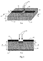
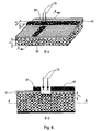
- Figure 1 schematically shows the structure conventional photocwitches, as they are currently produced.
- FIG. 1-a is a schematic overview of a photoc switch.
- This photocututor consists of a conductive strip of width w having a discontinuity 13 between its two conductive elements 11 and 12.
- This conductive strip is placed on a semiconductor substrate 14 of thickness "e".
- These conductive elements 11 and 12 are separated from each other by the discontinuity 13 of length I g , called Gap.
- the structure of the photocutter is completed by a ground plane 17 located on the face of the substrate opposite to that which carries the conductive strip.
- the face of the substrate carrying the conductive strip will be called “upper face", as opposed to the face bearing the ground plane to be called “lower face”.
- the semiconductor substrate has at rest a very low conductivity and the photoc switch then behaves as an open circuit preventing the propagation of a signal through the conductive strip.
- the conductive strip is an element of a transmission line
- the transmission of the signal on the line is then interrupted.
- the semiconductor substrate area located at the level of the Gap is subjected to illumination 15, the semiconductor sees its conduction properties change locally. In this zone, he becomes a conductor whose resistance varies with illumination.
- the photocommutator then behaves like a resistive circuit that lets the electrical signals propagate on the line.
- FIG. 1-b shows a diagrammatic sectional view of the same photocontr switch when it is subjected to illumination 15.
- This zone is created by photoconduction.
- Its thickness e c is in particular a function of the absorption coefficient value of the substrate, for the wavelength of the source responsible for the illumination.
- the photoconduction zone 16 may for example have a thickness e c of a few tens of microns for a substrate thickness of the order of a hundred microns.
- the value of the conductance of the photoconduction zone 16 is in particular a function of the value of the illumination to which it is subjected.
- the photoconduction phenomenon is of interest only if the photoconduction zone has a size at least equal to the length I g separating the conductive elements.
- the illumination must therefore be realized in this direction. In the remainder of the description, it is considered that this is the case and that, in the presence of illumination, the local conduction zone formed in the substrate ensures the connection of the conductive elements 11 and 12.
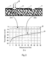
- FIG 2 illustrates the frequency behavior of Current photocwitches, in their two “ON” operating states and "OFF".
- Figure 2-a illustrates pictorially the function performed by a photocommutator when it is subjected to the level of the discontinuity zone at an illumination whose wavelength is absorbed by the substrate.
- the illumination of the substrate induces the appearance a conductive zone 16, or photoconduction zone, whose frequency behavior is substantially that of a resistance 21 put in series between the conductive elements 11 and 12 of the conductive strip. Since the value of the resistor 21 is not too high, the photocommutator can be likened to a short circuit, which represents the function performed by a closed switch.
- Curve 22 of FIG. 2-c gives us an example of this resistive behavior, for a photocut switch made on a Gallium Arsenide substrate and having a Gap of length I g equal to 100 ⁇ m.
- the switch In the state "ON" the switch is presented as a resistive element worth in the example a hundred ohms.
- the transmittance is substantially constant over the entire frequency band analyzed, between 0 Hz and 50 GHz.
- Figure 2-b illustrates the function performed by the same light switch when the Gap is not subjected to adequate illumination. This is for example the case when it is in the dark or when it is exposed to the light of the day.
- the function that one wishes to perform is an open circuit, having a substantially zero conductance.
- the measurements carried out show that we can assimilate the currently developed photocwitches, much more to capacitive elements 23 than to open circuits. Their frequency response is variable. Moreover, it is increasing according to the frequency.
- Curve 24 of FIG. 2-c gives us an example of this capacitive behavior, for a photocut switch made on a Gallium Arsenide substrate and having a Gap of length I g equal to 100 ⁇ m.
- the switch In the "OFF" state, the switch is a capacitive element.
- the transmittance is initially very low in the vicinity of the Giga Hertz then increases substantially with the frequency.
- the photocutter therefore has a behavior substantially closer to a high-pass circuit than an open circuit.
- This parasitic capacitive effect has the effect of degrading very strongly the breaking performance of the current photocwitches. It makes their use difficult or impossible in assemblies operating at frequencies above a few Giga Hertz. If we consider the example of Figure 2 - c, we see that at a frequency of 10 GHz the cutoff ratio which figures the difference in transmittance between the "ON" state and the "OFF” state presented by a Photocoupler is less than 40dB. It even becomes less than 30dB when the frequency is around 20GHz. The cutoff function is then poorly assured.
- the parasitic capacitive effect which becomes predominant as the frequency increases, has the effect of limiting the bandwidth of use of the current photocwitches.
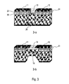
- Figure 3 presents two possible examples of realizations of photocwitches according to the invention.
- obtaining good isolation at frequencies is obtained by decreasing the value of the parasite capacity present in the Gap area.
- the result is achieved by minimizing the value of parasitic capacitance related to the proximity of the substrate on which is laid the conductive strip.
- the Gap is isolated from the substrate medium of a layer of air. It tends to reduce the influence of the substrate and to reduce the value of this parasitic capacitance to that of the capacity specific to the Gap structure, this capacity being of low value. For to obtain this result several structures are possible.
- Figure 3-a shows a possible embodiment in which a layer of dielectric material 31 is interposed between the conductive strip and the substrate.
- This layer whose permittivity is much lower than that of substrate, may consist of two sub-layers 32 and 33: a layer Nitride and a polyamide layer for example.
- This dielectric layer offers the advantage of reducing the value of the bonding capacitors existing between the elements 11 and 12 of the conductive strip and the substrate. It is equivalent in particular to a series of capacitances of lower values with the capacity induced by the substrate.
- the dielectric layer is locally interrupted in the area of the Gap and thus leaves room for an air layer 34 between the substrate and the Gap.
- the local interruption of the dielectric layer at the gap and its replacement by a layer of air advantageously reduces the value of the parasitic capacitance, the permittivity of the air being close to that of the vacuum.
- the local interruption of the dielectric layer at the Gap also has another advantage.
- the gap zone also corresponds to the photoconduction zone of the substrate.
- the presence in this zone of a layer of dielectric material can be a source of a strong reflection of the illuminating radiation, at the interface between the substrate 14 and the layer 31 of dielectric material. Removing the dielectric layer thus ensures optimum illumination conditions.
- Figure 3-b shows another possible embodiment of a photoc switch according to the invention.
- the elements 11 and 12 of the conductive strip rest on a layer of dielectric material.
- this dielectric layer is interrupted at the level of the Gap, thus making it possible, in the gap zone, to isolate the conductive strip from the substrate by means of an air layer 34.
- the thickness reduction of the portion 35 of the substrate located under the Gap is performed on the underside of the substrate. In this way it is possible to make a greater reduction in thickness than in the previous embodiment, without impairing the operation of the photoc switch, especially in the "ON" state.
- a substrate thickness substantially equal to the thickness of the photoconduction zone can be left. This embodiment notably makes it possible to significantly reduce the value of parasitic capacitance, directly related to the thickness of the substrate.
- This reduction in the thickness of the substrate in the Gap zone is also accompanied by a clipping of the ground plane.
- This clipping allows access to the substrate by the underside of the circuit. So, in the as the thickness of the substrate in the area of the Gap is reduced to the absorption thickness of the radiation that illuminates the substrate, it is possible to realize the illumination of the substrate by the lower face.
- the interruption of the dielectric layer extends over more important than in the previous mode.
- the dielectric layer thus leaves instead of a layer of air 34 which surrounds the Gap more widely and which reinforces advantageously, isolation of the Gap with respect to the substrate.
- the two embodiments described here are based on a multilayer structure which have the advantage of significantly reducing the parasitic capacitance value.
- This multilayer structure is advantageously completed by the reduction of the thickness of the substrate layer at the level of the substrate. Gap.
- this multilayer structure provides a greatly improved cutoff ratio.
- the operation of the photocommutator in the "OFF" state is comparable in terms of insulation to that of a conventional switch, of the mechanical type for example. Thanks to the type of structure according to the invention shown in FIG. 3, it is for example possible to produce ultra-fast photocwitches, having a cut-off ratio between the "ON" state and the "OFF" state of about one.
- photocwitches are controlled by optical signals generally from laser sources whose wavelength is a function of the material constituting the substrate. It is thus possible for example to produce photocwitches whose switching is controlled by illumination at a wavelength of around 860 nm.
- Such photocommutators are in particular made on substrates of simple gallium arsenide, obtained for example by simple epitaxial growth or on Gallium arsenide low temperature substrates (GaAs BT).
- GaAs BT Gallium arsenide low temperature substrate has the advantage of offering a higher absorption of the illuminating radiation than standard gallium arsenide as well as lower switching times, of the order of the femtosecond.
- photocwitches whose switching is controlled by illumination at a wavelength located for example around 1.55 microns.
- the substrate used is a mixture of Gallium and indium combined with Arsenic (In 0.53 Ga 0.47 As). This substrate has good absorption of radiation around this wavelength.
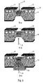
- Figure 4 shows typical examples of how photocwitches according to the invention. These exemplary embodiments the structure described in Figure 3-a and presents different solutions to illuminate the substrate in the area of the Gap.
- the illumination of the substrate zone situated at the level of the Gap is effected directly by the upper face of the circuit.
- the substrate receives all of the emitted radiation.
- This simple embodiment can for example be advantageously used in the case where it is desired to make a device comprising a single photocututor. Since the source is located near the gap, the transmission of the light signal can be done directly.
- the source may for example be positioned opposite the Gap by means of a structure not described here.
- FIG. 4-b shows another embodiment in which the illumination 15 of the substrate is made internally, by means of radiation guided to inside the substrate.
- the guidance of the radiation may for example be realized by integrating an optical waveguide structure into the substrate.
- This embodiment more complex than the previous one, has the advantage to integrate the illumination device with the structure of the circuit carrying the photoswitch.
- the light source can in particular be deported and connected to the circuit using the appropriate connector.
- FIG. 4-c presents an embodiment that makes it possible to illuminate a plurality of substrate zones with a single source. In this way, it is possible, in this way, to produce a plurality of photo-switches controlled from the same optical signal.
- This optical signal is for example guided to the different photocutters by an optical guiding device 42 located on the upper face of the circuit.
- This guiding device has the particularity of having semi-reflecting portions 43 in the zone of the Gaps of the different photocwitches.
- the light source is in this case connected to the structure integrating the photocwitches using appropriate connectors.
- this embodiment has the advantage of making it possible to control several photocwitches from the same optical signal. If the length of the optical paths is chosen judiciously, it is possible in particular to perform sampling of an electrical signal at different times in the same period of the signal.
- Figure 5 shows typical embodiments of photocwitches according to the invention which implement the structure described in Figure 3-b.
- This structure which involves a reduction of the thickness of the substrate in the area of the Gap, makes it possible to illumination which modifies in this zone the conductivity of the substrate on any its thickness.
- Illumination is here made directly by a suitable light source.
- Figure 5-c shows a more integrated structure which advantageously takes advantage of the accessibility of the substrate to illumination by the lower face.
- the illumination of the substrate is not directly achieved by the source but by means of a device 51 such as for example an optical waveguide.
- This type of embodiment has the particular advantage of integrating the illumination device, the structure of the circuit that carries the photocututor.
- such an embodiment advantageously makes it possible to control several photocwitches from a single optical signal.
- This type of embodiment also has the advantage of not covering the upper face of the circuit. It thus leaves free access to this face.
- FIGS. 4 and 5 The types of realization shown in FIGS. 4 and 5 are given here as an example and do not of course represent a state exhaustive. Other types of realization based on the structures presented Figure 3 is conceivable, in particular with regard to the way in which to expose the substrate to appropriate illumination. Moreover, for the sake of clarity, the representations in Figures 4 and 5 show isolated photocwitches. Nevertheless, the types of realization presented in examples are obviously intended to be integrated on the same circuit with other devices, including other photocwitches or other electronic devices.
- the photocwitches according to the invention allow very low switching times, a few hundreds of picoseconds for example, and a decoupling of the order of one fifty decibels between the "ON" state and the "OFF” state for a frequency around 20 GHz.
- They have a high bandwidth that can especially reach 50GHz. They can therefore advantageously be used in various fixtures in place of mechanical switches or electromechanical devices, such as in the case of structural circuits microstrip.
- the properties of the photocwitches according to the invention can be used in various electronic assemblies. These photocwitches can naturally be used as sampling circuits at very high speed and allow for example the direct sampling of a signal on a microwave carrier. They can still be inserted into the feedback loop of an amplifier circuit and play the role of a gain control circuit. In that case, the switch is for example used in the "ON" state. The variation of the value of the equivalent resistance of the switch as a function of the value of the illumination provided to the substrate is used to modify the value of the gain of the amplifier. An amplifier whose gain is controlled by an optical signal is thus obtained.
- the photocwitches according to the invention can also be used as tuning circuits that can be controlled in oscillator assemblies or else as phase-shifting elements. In both cases it is in particular the capacitive element related to the structure of the photocututor which is used.
- the use cases of photocwitches according to the invention mentioned here are given by way of examples. They are obviously not an exhaustive list.
- FIG. 6 illustrates a particular form of the device according to the invention.
- the photocurrent device according to the invention is used in particular to restore to order the continuity of a conductive line with a discontinuity 13.
- the device makes it possible, for example, to perform on controls the connection of two separate lines
- FIG. 6-a shows an exemplary structure with two perpendicular conducting lines 61 and 62 separated by a connection zone 63, of width substantially equivalent to that of the discontinuity zone 13 existing in the form of the device described above.
- the connection zone plays essentially the same role as the discontinuity zone. It is in this zone that illumination is applied.
- the role filled by the device according to the invention remains the same as in the form described above, as well as its mode of operation.
- the connection zone is an open circuit, the two lines being electrically insulated from each other.
- the connection zone is subjected to an appropriate illumination, it then appears as a short circuit connecting the two lines. The conduction is then performed through the substrate become locally conductive.
- the photoc switch set up at the connection zone 63 has a structure substantially identical to that of the photoc switch set up at the level of the discontinuity zone 13 of FIG. example.
- the device thus retains its advantageous properties mentioned in the foregoing description, particularly with regard to the isolation of the two lines in the absence of illumination.
- the relative arrangement of the two lines, perpendicular to each other, is presented here as an example and is in no way restrictive. The approximation of the two lines can be done in any angle, the only important characteristic being the existence of a connection zone
- This particular form of the device according to the invention advantageously finds its utility in the realization of certain electronic functions on MMIC circuits. It is for example possible to advantageously use the device according to the invention taken in this form, to achieve an attenuator whose attenuation value is controllable. To do this, it is sufficient, for example, to connect the end of the line 62 opposite the connection area to the ground of the circuit and to vary the value of the illumination to which the connection zone is subjected. Thus the level of the signal propagating on line 61 will be weakened by the signal level taken by line 62 and leads to ground. If the illumination becomes sufficient the signal propagating on the line 61 is then substantially grounded. It is also possible to advantageously use the device taken in this form as summing device. In this case the line 62 is of course not connected to the ground of the circuit but conveys a signal. This signal will be combined with the signal propagating on line 61, once the connection zone has been subjected to adequate illumination.
Landscapes
- Electronic Switches (AREA)
Abstract
Description
Ce dispositif est par exemple destiné à être associé à des circuits micro-ondes actifs.
Lors de l'illumination d'un élément photoconducteur il se produit une interaction entre les photons émis par la source de lumière et les atomes constituant l'élément photoconducteur. Les atomes ainsi excités voient leurs électrons situés dans la bande de valence passer dans la bande de conduction. Cette modification induit une modification de la conductivité de l'élément par effet de photoconduction. La modification apportée à l'élément est par nature réversible et cesse dès que l'illumination cesse. Les électrons ayant changé de bande d'énergie retournent alors à leur niveau initial.
L'état isolant ou état "OFF" correspond à l'état dans lequel se trouve l'élément semi-conducteur quand il n'est pas éclairé ou quand il reçoit un éclairement dont la longueur d'onde ne satisfait pas la relation (1). Dans cet état l'élément photoconducteur possède une conductance constante, très faible voire sensiblement nulle.
L'état conducteur ou état "ON" correspond à l'état opposé dans lequel se trouve l'élément semi-conducteur quand il est convenablement éclairé. Dans cet état l'élément photoconducteur voit sa conductance augmenter considérablement. Il se comporte donc comme un conducteur de faible résistance. Généralement, lors du passage à l'état "ON", l'éclairement reçu par l'élément photoconducteur est suffisant pour l'amener à une conductance proche de sa valeur maximum.
En l'absence d'éclairement à une longueur d'onde appropriée l'élément photoconducteur est isolant. Il bloque alors la transmission du signal véhiculé par la ligne de transmission dans laquelle il est inséré. En revanche, en présence d'éclairement il devient conducteur et assure ainsi la transmission du signal.
En éclairant la zone de substrat située à l'endroit d'une discontinuité, il est possible de rétablir par photoconduction la continuité de la ligne. Le signal franchit alors la zone discontinue au travers du substrat devenu localement conducteur.
De tels photocommutateurs présentent dans leur principe de nombreux avantages. Ils peuvent notamment être implantés au sein de stuctures de type microruban et donc être facilement intégrés à des circuits actifs. Ils ont de plus des temps de commutation très faibles. Ils ne comportent pas, à la différence des commutateurs électromécaniques, de pièces mécaniques en mouvement et bénéficient ainsi d'un encombrement plus réduit et d'une plus longue durée de vie. Ils sont en outre peu sensibles aux perturbations.
En revanche les photocommutateurs réalisés actuellement présentent l'inconvénient d'offrir un isolement insuffisant à l'état "OFF", lorsque la fréquence du signal dont on veut empêcher la propagation dépasse par exemple quelques Gigahertz. Dans ce cas on assiste à une propagation parasite du signal dans la zone de discontinuité de la bande conductrice. La fonction de coupure n'est alors plus assurée convenablement.
Le dispositif a notamment pour avantage de diminuer sensiblement la valeur des capacités parasites induites dans les zones de discontinuité entre les éléments conducteurs et le substrat. Il accroít ainsi la gamme de fréquence dans laquelle on peut utiliser un commutateur optoélectronique.
Par sa structure le dispositif permet de réaliser plusieurs commutateurs commandés à partir d'un même signal optique.
D'autres caractéristiques et avantages apparaítront au travers de la description qui suit. Cette description est réalisée en regard des figures qui sont annexées et qui représentent :
Le substrat semi-conducteur possède au repos une conductivité très faible et le photocommutateur se comporte alors comme un circuit ouvert empêchant la propagation d'un signal au travers de la bande conductrice. Dans le cas où la bande conductrice est un élément d'une ligne de transmission, la transmission du signal sur la ligne est alors interrompue.
Quand la zone de substrat semi-conducteur située au niveau du Gap est soumise à un éclairement 15, le semi-conducteur voit ses propriétés de conduction se modifier localement. Dans cette zone, il devient un conducteur dont la résistance varie avec l'éclairement. Le photocommutateur se comporte alors comme un circuit résistif qui laisse se propager les signaux électriques sur la ligne.
La valeur de la conductance de la zone de photoconduction 16 est notamment fonction de la valeur de l'éclairement auquel elle est soumise.
Dans ce cas, la fonction que l'on souhaite réaliser est un circuit ouvert, ayant une conductance sensiblement nulle. Or les mesures effectuées montrent qu'on peut assimiler les photocommutateurs actuellement développés, bien plus à des éléments capacitifs 23 qu'à des circuits ouverts.
Leur réponse en fréquence est variable. De plus, elle est croissante en fonction de la fréquence.
La courbe 24 de la figure 2-c nous donne un exemple de ce comportement capacitif, pour un photocommutateur réalisé sur un substrat en Arséniure de Gallium et présentant un Gap de longueur Ig égale à 100µm.
Cet effet capacitif parasite a pour effet de dégrader très fortement les performances de coupure des photocommutateurs actuels. Il rend leur emploi difficile voire impossible dans des montages fonctionnant à des fréquences supérieures à quelques Giga Hertz.
Si on considère l'exemple de la figure 2 - c, on constate qu'à une fréquence de 10 GHz le rapport de coupure qui chiffre la différence de transmittance entre l'état "ON" et l'état "OFF" présenté par un photocommutateur est inférieure à 40dB. Il devient même inférieur à 30dB quand la fréquence avoisine les 20GHz. La fonction de coupure est alors mal assurée. L'effet capacitif parasite qui devient prépondérant à mesure que la fréquence augmente, a pour conséquence de limiter la bande passante d'utilisation des photocommutateurs actuels.
- La structure même du Gap constitué des extrémités des deux éléments 11 et 12 de la bande conductrice et de la zone de discontinuité qui les sépare. Cette structure est celle d'un condensateur à air, dont la capacité est par ailleurs très faible.
- La nature du substrat semi-conducteur dont la permittivité relative εr est de l'ordre de 10. Cette valeur élevée de εr se traduit notamment par l'existence d'un effet capacitif parasite important au niveau du substrat.
La couche diélectrique est localement interrompue dans la zone du Gap et laisse ainsi sa place à une couche d'air 34 entre le substrat et le Gap.
L'interruption locale de la couche diélectrique au niveau du gap et son remplacement par une couche d'air contribue avantageusement à diminuer la valeur de la capacité parasite, la permittivité de l'air étant voisine de celle du vide.
L'interruption locale de la couche diélectrique au niveau du Gap présente également un autre avantage. La zone du gap correspond également à la zone de photoconduction du substrat. Or la présence dans cette zone d'une couche de matériau diélectrique peut être source d'une forte réflexion du rayonnement éclairant, à l'interface entre le substrat 14 et la couche 31 de matériau diélectrique. Supprimer la couche diélectrique permet donc de garantir des conditions d'éclairement optimales.
Dans ce mode de réalisation, la réduction de l'épaisseur du substrat dans la zone 35 est réalisée sur la face supérieure du substrat. La zone 36 correspondant à une réduction de l'épaisseur du substrat, forme une couche d'air supplémentaire qui accroít l'isolement de la zone du Gap vis à vis du substrat.
Dans ce mode de réalisation, la valeur maximale de la réduction de l'épaisseur du substrat est limitée par la nécessité de conserver les caractéristiques du photocommutateur. L'épaisseur de la zone 36 laissée vide ne doit en effet pas nuire au fonctionnement du commutateur notamment à l'état "ON". Une zone 36 de taille trop importante donnerait notamment un caractère capacitif à l'état "ON", état que l'on souhaite avant tout résistif.
Dans ce mode de réalisation comme dans celui de la figure 3-a, les éléments 11 et 12 de la bande conductrice reposent sur une couche de matériau diélectrique. De même, cette couche diélectrique est interrompue au niveau du Gap, permettant ainsi, dans la zone du gap, d'isoler la bande conductrice du substrat par l'intermédiaire d'une couche d'air 34.
En revanche, à la différence du mode de réalisation précédent, la réduction d'épaisseur de la partie 35 du substrat située sous le Gap est réalisée sur la face inférieure du substrat. De cette façon il est possible d'opérer une réduction d'épaisseur plus importante que dans le mode de réalisation précédent, sans altérer le fonctionnement du photocommutateur, en particulier à l'état "ON". On peut par exemple laisser une épaisseur de substrat sensiblement égale à l'épaisseur de la zone de photoconduction.
Ce mode de réalisation permet notamment de réduire de manière sensible la valeur de la capacité parasite, directement liée à l'épaisseur du substrat.
Grâce au type de structure selon l'invention présenté à la figure 3, il est par exemple possible de réaliser des photocommutateurs ultra rapides, présentant un rapport de coupure entre l'état "ON" et l'état "OFF" d'environ une cinquantaine de dB à une fréquence se situant autour de 20 GHz.
Ces photocommutateurs sont commandés par des signaux optiques généralement issus de sources laser dont la longueur d'onde est fonction du matériau constituant le substrat.
On peut ainsi par exemple réaliser des photocommutateurs dont la commutation est commandée par un éclairement à une longueur d'onde située autour de 860 nm. De tels photocommutateurs sont notamment réalisés sur des substrats d'arséniure de Gallium simple, obtenu par exemple par simple croissance épitaxiale ou encore sur des substrats d'arséniure de Gallium Basse Température (GaAs BT). Un substrat d'arséniure de Gallium Basse Température présent l'avantage d'offrir une absorption plus forte du rayonnement éclairant que l'arséniure de Gallium standard ainsi que de plus faibles temps de commutation, de l'ordre de la femtoseconde.
On peut également réaliser des photocommutateurs dont la commutation est commandée par un éclairement à une longueur d'onde située par exemple autour de 1.55 µm. Dans ce cas le substrat utilisé est un mélange de Gallium et d'indium combiné à l'Arsenic (In0.53Ga0.47As). Ce substrat présente une bonne absorption des rayonnements autour de cette longueur d'onde.
Ce mode simple de réalisation peut par exemple être avantageusement utilisé dans le cas où l'on souhaite réaliser un dispositif comportant un seul photocommutateur. La source étant située à proximité du gap, la transmission du signal lumineux peut se faire de manière directe. La source peut par exemple être positionnée en regard du Gap au moyen d'une structure non décrite ici.
Comme il a été dit précédemment, ce mode de réalisation présente l'avantage de rendre possible la commande de plusieurs photocommutateurs à partir d'un même signal optique. Si la longueur des chemins optiques est choisie judicieusement, il est notamment possible de réaliser un échantillonnage d'un signal électrique à des instants différents dans une même période du signal.
Ce type de réalisation présente notamment l'avantage d'intégrer le dispositif d'éclairement, à la structure du circuit qui porte le photocommutateur. De plus comme dans le mode de réalisation présenté à la figure 4-c, un tel mode de réalisation rend avantageusement possible la commande de plusieurs photocommutateurs à partir d'un seul signal optique. Ce type de réalisation présente encore l'avantage de ne pas recouvrir la face supérieure du circuit. Il laisse ainsi libre accès à cette face.
Ces photocommutateurs peuvent naturellement être utilisés comme circuits échantillonneurs à très grande rapidité et permettre par exemple l'échantillonnage direct d'un signal sur une porteuse hyperfréquence.
Ils peuvent encore être insérés dans la boucle de réaction d'un montage amplificateur et jouer le rôle d'un circuit de commande de gain. Dans ce cas,
le commutateur est par exemple employé à l'état "ON". La variation de la valeur de la résistance équivalente du commutateur en fonction de la valeur de l'éclairement apporté au substrat, est utilisée pour modifier la valeur du gain de l'amplificateur. On obtient ainsi un amplificateur dont le gain est commandé par un signal optique.
Les photocommutateurs selon l'invention peuvent également être utilisés comme circuits d'accord commandables dans des montages oscillateurs ou encore comme éléments déphaseurs. Dans ces deux cas c'est notamment l'élément capacitif lié à la structure du photocommutateur qui est mis à profit.
Les cas d'emploi de photocommutateurs selon l'invention cités ici sont donnés à titre d'exemples. Ils ne constituent évidemment pas une liste exhaustive.
Le rôle rempli par le dispositif selon l'invention reste le même que dans la forme décrite précédemment, ainsi que son mode de fonctionnement. En l'absence d'éclairement la zone de connexion se présente comme un circuit ouvert, les deux lignes étant électriquement isolées l'une de l'autre. En revanche si la zone de connexion est soumise à un éclairement approprié elle se présente alors comme un court circuit qui relie les deux lignes. La conduction est alors réalisée au travers du substrat devenu localement conducteur.
De ce fait, les modes de réalisation illustrés par les figures 3, 4 et 5 restent valables pour la réalisation du dispositif dans cette forme particulière, adaptée notamment à la connexion de deux lignes. Le dispositif conserve ainsi ses propriétés avantageuses citées dans la description qui précède, notamment en ce qui concerne l'isolement des deux lignes en l'absence d'éclairement.
La disposition relative des deux lignes, perpendiculairement l'une à l'autre, est présentée ici à titre d'exemple et n'est en rien restrictive. Le rapprochement des deux lignes peut notamment se faire sous un angle quelconque, la seule caractéristique importante étant l'existence d'une zone de connexion
Il est par exemple possible d'utiliser avantageusement le dispositif selon l'invention pris sous cette forme, pour réaliser un atténuateur dont la valeur de l'atténuation est commandable. Pour ce faire il suffit par exemple de relier à la masse du circuit l'extrémité de la ligne 62 opposée à la zone de connexion et de faire varier la valeur de l'éclairement auquel est soumise la zone de connexion. Ainsi le niveau du signal se propageant sur la ligne 61 se verra affaibli du niveau de signal prélevé par la ligne 62 et conduit à la masse. Si l'éclairement devient suffisant le signal se propageant sur la ligne 61 est alors sensiblement mis à la masse.
Il est également possible d'utiliser avantageusement le dispositif pris sous cette forme comme dispositif sommateur. Dans ce cas la ligne 62 n'est bien sûr pas reliée à la masse du circuit mais véhicule un signal. Ce signal sera combiné au signal se propageant sur la ligne 61, dès lors que la zone de connexion aura été soumise à un éclairement adéquat.
Claims (20)
- Dispositif de commutation optoélectronique, caractérisé en ce que sa structure comporte au moins :deux éléments conducteurs espacés l'un de l'autre,une couche diélectrique (31) à faible permittivité relative sur laquelle sont appliqués les éléments conducteurs,une couche de substrat semi-conducteur sur laquelle sont appliqués la couche diélectrique et les éléments conducteurs,des moyens d'éclairement qui illuminent au moins une partie l'espace séparant les deux éléments conducteurs sur une zone de photoconduction (16) s'étendant au moins d'un élément conducteur à l'autre et qui modifient la conductivité du substrat dans la zone de photoconduction pour le rendre localement conducteur.
- Dispositif selon la revendication 1, caractérisé en ce que les deux éléments conducteurs constituent les deux éléments (11 et 12) d'une ligne conductrice unique présentant une discontinuité (13), la zone de photoconduction (16) étant située au niveau de la discontinuité.
- Dispositif selon la revendication 1, caractérisé en ce les deux éléments conducteurs constituent deux lignes conductrices (61 et 62) distinctes bordant la zone de photoconduction (16).
- Dispositif selon l'une quelconque des revendications précédentes, caractérisé en ce qu'à l'endroit de la zone de photoconduction (16) la couche diélectrique est interrompue sur une zone incluant la zone de photoconduction et est remplacée par une couche d'air (34) permettant d'isoler les éléments conducteurs vis à vis substrat dans la zone d'éclairement.
- Dispositif selon la revendication précédente, caractérisé en ce que la couche d'air est transparente pour le signal optique et permet d'obtenir un éclairement du substrat sans réflexion.
- Dispositif selon l'une quelconque des revendications précédentes, caractérisé en ce qu'au niveau de la zone de photoconduction l'épaisseur du substrat est réduite afin de diminuer la valeur de la capacité parasite liée au substrat.
- Dispositif selon l'une quelconque des revendications précédentes, caractérisé en ce que la réduction de l'épaisseur du substrat est réalisée sur la face supérieure du substrat, l'espace libéré formant une couche d'air (36).
- Dispositif selon l'une quelconque des revendications précédentes, caractérisé en ce que l'éclairement (15) du substrat est réalisé par un signal optique issu d'une source éclairant directement le substrat par la face supérieure du circuit.
- Dispositif selon la revendication précédente, caractérisé en ce que la source éclairant le substrat est une fibre optique.
- Dispositif selon l'une quelconque des revendications 1 à 5, caractérisé en ce que l'éclairement (15) du substrat est réalisé par un signal optique véhiculé par un guide d'onde optique (42) placé sur la face supérieure du circuit.
- Dispositif selon la revendication précédente, caractérisé en ce que le guide d'onde optique (42) distribue le signal optique à plusieurs dispositifs.
- Dispositif selon l'une quelconque des revendications 1 à 5, caractérisé en ce que l'éclairement (15) du substrat est réalisé par un signal optique véhiculé par un guide d'onde optique (41) intégré au substrat, à une profondeur sensiblement égale à l'épaisseur d'absorption du substrat pour la longueur d'onde considérée.
- Dispositif selon l'une quelconque des revendications 1 à 4, caractérisé en ce que la réduction de l'épaisseur du substrat est réalisée sur la face inférieure du substrat, l'épaisseur du substrat dans la zone de photoconduction étant sensiblement égale à l'épaisseur d'absorption du substrat pour la longueur d'onde correspondant à l'éclairement.
- Dispositif selon la revendication précédente caractérisé en ce que l'éclairement (15) du substrat est réalisé par un signal optique issu d'une source éclairant directement le substrat indifféremment par la face supérieure ou la face inférieure du circuit.
- Dispositif selon la revendication précédente, caractérisé en ce que la source éclairant le substrat est une fibre optique.
- Dispositif selon la revendication 11, caractérisé en ce que l'éclairement (15) du substrat est réalisé par un signal optique véhiculé par un guide d'onde optique situé indifféremment sur la face supérieure ou la face inférieure du circuit.
- Application du dispositif selon l'une quelconque des revendications précédentes, à l'échantillonnage ultra rapide de signaux hyperfréquence se propageant sur la ligne conductrice.
- Application du dispositif selon l'une quelconque des revendications 1 à 14, à la commande de gain d'amplificateurs par exemple hyperfréquence.
- Application du dispositif selon l'une quelconque des revendications 1 à 14, à la réalisation de circuits déphaseurs par exemple hyperfréquence.
- Application du dispositif selon l'une quelconque des revendications 1 à 14, à la réalisation de circuits oscillateurs commandables en fréquence.
Applications Claiming Priority (2)
| Application Number | Priority Date | Filing Date | Title |
|---|---|---|---|
| FR0208129A FR2841708B1 (fr) | 2002-06-28 | 2002-06-28 | Commutateur optoelectronique ultra rapide a grand pouvoir d'isolement et large bande passante |
| FR0208129 | 2002-06-28 |
Publications (2)
| Publication Number | Publication Date |
|---|---|
| EP1387409A1 true EP1387409A1 (fr) | 2004-02-04 |
| EP1387409B1 EP1387409B1 (fr) | 2016-04-20 |
Family
ID=29724996
Family Applications (1)
| Application Number | Title | Priority Date | Filing Date |
|---|---|---|---|
| EP03101866.6A Expired - Lifetime EP1387409B1 (fr) | 2002-06-28 | 2003-06-25 | Commutateur optoélectronique ultra rapide à grand pouvoir d'isolement et large bande passante |
Country Status (2)
| Country | Link |
|---|---|
| EP (1) | EP1387409B1 (fr) |
| FR (1) | FR2841708B1 (fr) |
Cited By (1)
| Publication number | Priority date | Publication date | Assignee | Title |
|---|---|---|---|---|
| CN111492583A (zh) * | 2017-08-29 | 2020-08-04 | 意法半导体有限公司 | 集成光学开关 |
Families Citing this family (2)
| Publication number | Priority date | Publication date | Assignee | Title |
|---|---|---|---|---|
| US10802375B2 (en) | 2017-09-15 | 2020-10-13 | Samsung Electronics Co., Ltd. | Optically-controlled switch |
| RU2691593C1 (ru) | 2018-09-20 | 2019-06-14 | Самсунг Электроникс Ко., Лтд. | Высокочастотные коммутаторы с уменьшенным числом коммутирующих элементов |
Citations (4)
| Publication number | Priority date | Publication date | Assignee | Title |
|---|---|---|---|---|
| US4403239A (en) * | 1979-12-26 | 1983-09-06 | Shunpei Yamazaki | MIS Type semiconductor photoelectric conversion device |
| JPS60142578A (ja) * | 1983-12-28 | 1985-07-27 | Matsushita Electric Ind Co Ltd | 光センサ |
| US4843446A (en) * | 1986-02-27 | 1989-06-27 | Hitachi, Ltd. | Superconducting photodetector |
| US5514996A (en) * | 1992-12-04 | 1996-05-07 | Kabushiki Kaisha Toshiba | Photo-coupler apparatus |
-
2002
- 2002-06-28 FR FR0208129A patent/FR2841708B1/fr not_active Expired - Fee Related
-
2003
- 2003-06-25 EP EP03101866.6A patent/EP1387409B1/fr not_active Expired - Lifetime
Patent Citations (4)
| Publication number | Priority date | Publication date | Assignee | Title |
|---|---|---|---|---|
| US4403239A (en) * | 1979-12-26 | 1983-09-06 | Shunpei Yamazaki | MIS Type semiconductor photoelectric conversion device |
| JPS60142578A (ja) * | 1983-12-28 | 1985-07-27 | Matsushita Electric Ind Co Ltd | 光センサ |
| US4843446A (en) * | 1986-02-27 | 1989-06-27 | Hitachi, Ltd. | Superconducting photodetector |
| US5514996A (en) * | 1992-12-04 | 1996-05-07 | Kabushiki Kaisha Toshiba | Photo-coupler apparatus |
Non-Patent Citations (4)
| Title |
|---|
| ITATANI T ET AL: "ULTRAFAST METAL-SEMICONDUCTOR-METAL PHOTOCONDUCTIVE SWITCHES FABRICATED USING AN ATOMIC FORCE MICROSCOPE", JAPANESE JOURNAL OF APPLIED PHYSICS, PUBLICATION OFFICE JAPANESE JOURNAL OF APPLIED PHYSICS. TOKYO, JP, vol. 35, no. 2B, PART 1, 1 February 1996 (1996-02-01), pages 1387 - 1389, XP000614759, ISSN: 0021-4922 * |
| PATENT ABSTRACTS OF JAPAN vol. 009, no. 305 (E - 363) 3 December 1985 (1985-12-03) * |
| PFEIFER T ET AL: "Picosecond Optoelectronic On-Wafer Characterization of Coplanar Waveguides on High-Resistivity Si and Si/SiO2 Substrates", MICROELECTRONIC ENGINEERING, ELSEVIER PUBLISHERS BV., AMSTERDAM, NL, vol. 31, no. 1, 1 February 1996 (1996-02-01), pages 385 - 395, XP004006650, ISSN: 0167-9317 * |
| TWAROWSKI K J ET AL: "PHOTOCONDUCTIVITY EFFECTS IN POLYCRYSTALLINE SILICON AND OPTICALLY CONTROLLED COPLANAR WAVEGUIDE SWITCH PHOTOCONDUCTIVITE DANS LE SILICIUM POLYCRISTALLIN;COMMUTATEUR EN GUIDE COPLANAIRE INTEGRE ET COMMANDE OPTIQUEMENT", ANNALES DES TELECOMMUNICATIONS - ANNALS OF TELECOMMUNICATIONS, PRESSES POLYTECHNIQUES ET UNIVERSITAIRES ROMANDES, LAUSANNE, CH, vol. 56, no. 3/4, March 2001 (2001-03-01), pages 208 - 214, XP001034548, ISSN: 0003-4347 * |
Cited By (2)
| Publication number | Priority date | Publication date | Assignee | Title |
|---|---|---|---|---|
| CN111492583A (zh) * | 2017-08-29 | 2020-08-04 | 意法半导体有限公司 | 集成光学开关 |
| CN111492583B (zh) * | 2017-08-29 | 2023-09-29 | 意法半导体有限公司 | 集成光学开关 |
Also Published As
| Publication number | Publication date |
|---|---|
| EP1387409B1 (fr) | 2016-04-20 |
| FR2841708B1 (fr) | 2005-07-01 |
| FR2841708A1 (fr) | 2004-01-02 |
Similar Documents
| Publication | Publication Date | Title |
|---|---|---|
| EP2110881B1 (fr) | Circulateur radiofréquence a base de mems | |
| EP0511913B1 (fr) | Dispositif optoélectronique à guide optique et photodétecteur intégrés | |
| FR3011346A1 (fr) | Dephaseur electro-optique a capacite d'oxyde | |
| EP3465724B1 (fr) | Membrane mems à ligne de transmission intégrée | |
| EP2178152A1 (fr) | Dispositif de commutation électronique pour signaux a haute fréquence | |
| EP1387409B1 (fr) | Commutateur optoélectronique ultra rapide à grand pouvoir d'isolement et large bande passante | |
| EP2351218B1 (fr) | Sonde atomique tomographique comportant un generateur electro-optique d'impulsions electriques haute tension | |
| EP0978949B1 (fr) | Dispositif de commutation de signaux radio-fréquences | |
| EP2862022B1 (fr) | Composant hyperfréquence commandé par un système d'électrodes coplanaires blindées, et procédé de fabrication correspondant | |
| EP4350890A1 (fr) | Commutateur a base d'un materiau a changement de phase | |
| FR2871951A1 (fr) | Dispositif de transition rntre un guide d'ondes et deux circuits redondants chacun couple a une ligne coplanaire | |
| EP2015391B1 (fr) | Atténuateur coaxial | |
| FR2916086A1 (fr) | Coupleur de signaux hyperfrequences en technologie microruban. | |
| EP0287010A1 (fr) | Oscillateur à resonateur diélectrique et accord électronique de fréquence par varactor, notamment dans la gamme des 22 GHz | |
| EP0524878A1 (fr) | Absorbeur hyperfréquence à semiconducteur et à commande optique | |
| CA2316934A1 (fr) | Composant electro-optique multi-sections | |
| FR3144489A1 (fr) | Composant de connexion radiofréquence supraconducteur | |
| FR3066858B1 (fr) | Procede pour minimiser une distorsion d'un signal dans un circuit radiofrequence | |
| EP1856573A1 (fr) | Modulateur a guide d´onde et procede de modulation associe | |
| EP2648335B1 (fr) | Limiteur de puissance hyperfréquence à commutateurs MEMS radiofréquences capacitifs | |
| WO2014057090A1 (fr) | Dispositif d'échantillonnage électro-optique d'un signal hyperfréquence. | |
| FR2930373A1 (fr) | Limiteur de puissance a base de mems. | |
| FR3146766A1 (fr) | Transition améliorée entre un contact central d’un composant coaxial et une ligne de transmission, notamment radiofréquence (RF). | |
| FR3059838A1 (fr) | Composant micro-ondes et procede de reglage associe | |
| WO1989004969A1 (fr) | Dispositif de caracterisation electrique d'echantillons et application a la cartographie electrique d'echantillons semi-conducteurs de grande surface |
Legal Events
| Date | Code | Title | Description |
|---|---|---|---|
| PUAI | Public reference made under article 153(3) epc to a published international application that has entered the european phase |
Free format text: ORIGINAL CODE: 0009012 |
|
| AK | Designated contracting states |
Kind code of ref document: A1 Designated state(s): AT BE BG CH CY CZ DE DK EE ES FI FR GB GR HU IE IT LI LU MC NL PT RO SE SI SK TR |
|
| AX | Request for extension of the european patent |
Extension state: AL LT LV MK |
|
| AKX | Designation fees paid | ||
| REG | Reference to a national code |
Ref country code: DE Ref legal event code: 8566 |
|
| 17P | Request for examination filed |
Effective date: 20040803 |
|
| RBV | Designated contracting states (corrected) |
Designated state(s): AT BE BG CH CY CZ DE DK EE ES FI FR GB GR HU IE IT LI LU MC NL PT RO SE SI SK TR |
|
| 17Q | First examination report despatched |
Effective date: 20140402 |
|
| GRAP | Despatch of communication of intention to grant a patent |
Free format text: ORIGINAL CODE: EPIDOSNIGR1 |
|
| INTG | Intention to grant announced |
Effective date: 20151204 |
|
| GRAS | Grant fee paid |
Free format text: ORIGINAL CODE: EPIDOSNIGR3 |
|
| RAP1 | Party data changed (applicant data changed or rights of an application transferred) |
Owner name: THALES |
|
| GRAA | (expected) grant |
Free format text: ORIGINAL CODE: 0009210 |
|
| AK | Designated contracting states |
Kind code of ref document: B1 Designated state(s): AT BE BG CH CY CZ DE DK EE ES FI FR GB GR HU IE IT LI LU MC NL PT RO SE SI SK TR |
|
| REG | Reference to a national code |
Ref country code: GB Ref legal event code: FG4D Free format text: NOT ENGLISH |
|
| REG | Reference to a national code |
Ref country code: CH Ref legal event code: EP |
|
| REG | Reference to a national code |
Ref country code: AT Ref legal event code: REF Ref document number: 793276 Country of ref document: AT Kind code of ref document: T Effective date: 20160515 |
|
| REG | Reference to a national code |
Ref country code: IE Ref legal event code: FG4D Free format text: LANGUAGE OF EP DOCUMENT: FRENCH |
|
| REG | Reference to a national code |
Ref country code: FR Ref legal event code: PLFP Year of fee payment: 14 |
|
| REG | Reference to a national code |
Ref country code: DE Ref legal event code: R096 Ref document number: 60348842 Country of ref document: DE |
|
| REG | Reference to a national code |
Ref country code: AT Ref legal event code: MK05 Ref document number: 793276 Country of ref document: AT Kind code of ref document: T Effective date: 20160420 |
|
| REG | Reference to a national code |
Ref country code: NL Ref legal event code: MP Effective date: 20160420 |
|
| PG25 | Lapsed in a contracting state [announced via postgrant information from national office to epo] |
Ref country code: NL Free format text: LAPSE BECAUSE OF FAILURE TO SUBMIT A TRANSLATION OF THE DESCRIPTION OR TO PAY THE FEE WITHIN THE PRESCRIBED TIME-LIMIT Effective date: 20160420 Ref country code: FI Free format text: LAPSE BECAUSE OF FAILURE TO SUBMIT A TRANSLATION OF THE DESCRIPTION OR TO PAY THE FEE WITHIN THE PRESCRIBED TIME-LIMIT Effective date: 20160420 |
|
| PG25 | Lapsed in a contracting state [announced via postgrant information from national office to epo] |
Ref country code: SE Free format text: LAPSE BECAUSE OF FAILURE TO SUBMIT A TRANSLATION OF THE DESCRIPTION OR TO PAY THE FEE WITHIN THE PRESCRIBED TIME-LIMIT Effective date: 20160420 Ref country code: GR Free format text: LAPSE BECAUSE OF FAILURE TO SUBMIT A TRANSLATION OF THE DESCRIPTION OR TO PAY THE FEE WITHIN THE PRESCRIBED TIME-LIMIT Effective date: 20160721 Ref country code: PT Free format text: LAPSE BECAUSE OF FAILURE TO SUBMIT A TRANSLATION OF THE DESCRIPTION OR TO PAY THE FEE WITHIN THE PRESCRIBED TIME-LIMIT Effective date: 20160822 Ref country code: ES Free format text: LAPSE BECAUSE OF FAILURE TO SUBMIT A TRANSLATION OF THE DESCRIPTION OR TO PAY THE FEE WITHIN THE PRESCRIBED TIME-LIMIT Effective date: 20160420 Ref country code: AT Free format text: LAPSE BECAUSE OF FAILURE TO SUBMIT A TRANSLATION OF THE DESCRIPTION OR TO PAY THE FEE WITHIN THE PRESCRIBED TIME-LIMIT Effective date: 20160420 |
|
| PG25 | Lapsed in a contracting state [announced via postgrant information from national office to epo] |
Ref country code: BE Free format text: LAPSE BECAUSE OF NON-PAYMENT OF DUE FEES Effective date: 20160630 |
|
| REG | Reference to a national code |
Ref country code: DE Ref legal event code: R097 Ref document number: 60348842 Country of ref document: DE |
|
| PG25 | Lapsed in a contracting state [announced via postgrant information from national office to epo] |
Ref country code: MC Free format text: LAPSE BECAUSE OF FAILURE TO SUBMIT A TRANSLATION OF THE DESCRIPTION OR TO PAY THE FEE WITHIN THE PRESCRIBED TIME-LIMIT Effective date: 20160420 Ref country code: CZ Free format text: LAPSE BECAUSE OF FAILURE TO SUBMIT A TRANSLATION OF THE DESCRIPTION OR TO PAY THE FEE WITHIN THE PRESCRIBED TIME-LIMIT Effective date: 20160420 Ref country code: RO Free format text: LAPSE BECAUSE OF FAILURE TO SUBMIT A TRANSLATION OF THE DESCRIPTION OR TO PAY THE FEE WITHIN THE PRESCRIBED TIME-LIMIT Effective date: 20160420 Ref country code: EE Free format text: LAPSE BECAUSE OF FAILURE TO SUBMIT A TRANSLATION OF THE DESCRIPTION OR TO PAY THE FEE WITHIN THE PRESCRIBED TIME-LIMIT Effective date: 20160420 Ref country code: DK Free format text: LAPSE BECAUSE OF FAILURE TO SUBMIT A TRANSLATION OF THE DESCRIPTION OR TO PAY THE FEE WITHIN THE PRESCRIBED TIME-LIMIT Effective date: 20160420 Ref country code: SK Free format text: LAPSE BECAUSE OF FAILURE TO SUBMIT A TRANSLATION OF THE DESCRIPTION OR TO PAY THE FEE WITHIN THE PRESCRIBED TIME-LIMIT Effective date: 20160420 |
|
| REG | Reference to a national code |
Ref country code: CH Ref legal event code: PL |
|
| PLBE | No opposition filed within time limit |
Free format text: ORIGINAL CODE: 0009261 |
|
| STAA | Information on the status of an ep patent application or granted ep patent |
Free format text: STATUS: NO OPPOSITION FILED WITHIN TIME LIMIT |
|
| REG | Reference to a national code |
Ref country code: IE Ref legal event code: MM4A |
|
| 26N | No opposition filed |
Effective date: 20170123 |
|
| PG25 | Lapsed in a contracting state [announced via postgrant information from national office to epo] |
Ref country code: LI Free format text: LAPSE BECAUSE OF NON-PAYMENT OF DUE FEES Effective date: 20160630 Ref country code: CH Free format text: LAPSE BECAUSE OF NON-PAYMENT OF DUE FEES Effective date: 20160630 |
|
| REG | Reference to a national code |
Ref country code: FR Ref legal event code: PLFP Year of fee payment: 15 |
|
| PG25 | Lapsed in a contracting state [announced via postgrant information from national office to epo] |
Ref country code: IE Free format text: LAPSE BECAUSE OF NON-PAYMENT OF DUE FEES Effective date: 20160625 Ref country code: SI Free format text: LAPSE BECAUSE OF FAILURE TO SUBMIT A TRANSLATION OF THE DESCRIPTION OR TO PAY THE FEE WITHIN THE PRESCRIBED TIME-LIMIT Effective date: 20160420 |
|
| REG | Reference to a national code |
Ref country code: FR Ref legal event code: PLFP Year of fee payment: 16 |
|
| PG25 | Lapsed in a contracting state [announced via postgrant information from national office to epo] |
Ref country code: CY Free format text: LAPSE BECAUSE OF FAILURE TO SUBMIT A TRANSLATION OF THE DESCRIPTION OR TO PAY THE FEE WITHIN THE PRESCRIBED TIME-LIMIT Effective date: 20160420 Ref country code: HU Free format text: LAPSE BECAUSE OF FAILURE TO SUBMIT A TRANSLATION OF THE DESCRIPTION OR TO PAY THE FEE WITHIN THE PRESCRIBED TIME-LIMIT; INVALID AB INITIO Effective date: 20030625 |
|
| PG25 | Lapsed in a contracting state [announced via postgrant information from national office to epo] |
Ref country code: LU Free format text: LAPSE BECAUSE OF NON-PAYMENT OF DUE FEES Effective date: 20160625 Ref country code: TR Free format text: LAPSE BECAUSE OF FAILURE TO SUBMIT A TRANSLATION OF THE DESCRIPTION OR TO PAY THE FEE WITHIN THE PRESCRIBED TIME-LIMIT Effective date: 20160420 |
|
| PG25 | Lapsed in a contracting state [announced via postgrant information from national office to epo] |
Ref country code: BG Free format text: LAPSE BECAUSE OF FAILURE TO SUBMIT A TRANSLATION OF THE DESCRIPTION OR TO PAY THE FEE WITHIN THE PRESCRIBED TIME-LIMIT Effective date: 20160420 |
|
| PGFP | Annual fee paid to national office [announced via postgrant information from national office to epo] |
Ref country code: FR Payment date: 20200526 Year of fee payment: 18 Ref country code: DE Payment date: 20200609 Year of fee payment: 18 |
|
| PGFP | Annual fee paid to national office [announced via postgrant information from national office to epo] |
Ref country code: IT Payment date: 20200527 Year of fee payment: 18 Ref country code: GB Payment date: 20200610 Year of fee payment: 18 |
|
| REG | Reference to a national code |
Ref country code: DE Ref legal event code: R119 Ref document number: 60348842 Country of ref document: DE |
|
| GBPC | Gb: european patent ceased through non-payment of renewal fee |
Effective date: 20210625 |
|
| PG25 | Lapsed in a contracting state [announced via postgrant information from national office to epo] |
Ref country code: GB Free format text: LAPSE BECAUSE OF NON-PAYMENT OF DUE FEES Effective date: 20210625 Ref country code: DE Free format text: LAPSE BECAUSE OF NON-PAYMENT OF DUE FEES Effective date: 20220101 |
|
| PG25 | Lapsed in a contracting state [announced via postgrant information from national office to epo] |
Ref country code: FR Free format text: LAPSE BECAUSE OF NON-PAYMENT OF DUE FEES Effective date: 20210630 |
|
| PG25 | Lapsed in a contracting state [announced via postgrant information from national office to epo] |
Ref country code: IT Free format text: LAPSE BECAUSE OF NON-PAYMENT OF DUE FEES Effective date: 20210625 |
|
| P01 | Opt-out of the competence of the unified patent court (upc) registered |
Effective date: 20230427 |