EP1387174A1 - Contact probe - Google Patents
Contact probe Download PDFInfo
- Publication number
- EP1387174A1 EP1387174A1 EP02718523A EP02718523A EP1387174A1 EP 1387174 A1 EP1387174 A1 EP 1387174A1 EP 02718523 A EP02718523 A EP 02718523A EP 02718523 A EP02718523 A EP 02718523A EP 1387174 A1 EP1387174 A1 EP 1387174A1
- Authority
- EP
- European Patent Office
- Prior art keywords
- alloy
- contact probe
- nickel
- electroforming
- cobalt
- Prior art date
- Legal status (The legal status is an assumption and is not a legal conclusion. Google has not performed a legal analysis and makes no representation as to the accuracy of the status listed.)
- Granted
Links
Images


Classifications
-
- G—PHYSICS
- G01—MEASURING; TESTING
- G01R—MEASURING ELECTRIC VARIABLES; MEASURING MAGNETIC VARIABLES
- G01R1/00—Details of instruments or arrangements of the types included in groups G01R5/00 - G01R13/00 and G01R31/00
- G01R1/02—General constructional details
- G01R1/06—Measuring leads; Measuring probes
- G01R1/067—Measuring probes
- G01R1/073—Multiple probes
- G01R1/07307—Multiple probes with individual probe elements, e.g. needles, cantilever beams or bump contacts, fixed in relation to each other, e.g. bed of nails fixture or probe card
- G01R1/07314—Multiple probes with individual probe elements, e.g. needles, cantilever beams or bump contacts, fixed in relation to each other, e.g. bed of nails fixture or probe card the body of the probe being perpendicular to test object, e.g. bed of nails or probe with bump contacts on a rigid support
-
- H—ELECTRICITY
- H10—SEMICONDUCTOR DEVICES; ELECTRIC SOLID-STATE DEVICES NOT OTHERWISE PROVIDED FOR
- H10P—GENERIC PROCESSES OR APPARATUS FOR THE MANUFACTURE OR TREATMENT OF DEVICES COVERED BY CLASS H10
- H10P74/00—Testing or measuring during manufacture or treatment of wafers, substrates or devices
-
- C—CHEMISTRY; METALLURGY
- C22—METALLURGY; FERROUS OR NON-FERROUS ALLOYS; TREATMENT OF ALLOYS OR NON-FERROUS METALS
- C22C—ALLOYS
- C22C19/00—Alloys based on nickel or cobalt
- C22C19/03—Alloys based on nickel or cobalt based on nickel
-
- C—CHEMISTRY; METALLURGY
- C22—METALLURGY; FERROUS OR NON-FERROUS ALLOYS; TREATMENT OF ALLOYS OR NON-FERROUS METALS
- C22C—ALLOYS
- C22C19/00—Alloys based on nickel or cobalt
- C22C19/07—Alloys based on nickel or cobalt based on cobalt
-
- C—CHEMISTRY; METALLURGY
- C25—ELECTROLYTIC OR ELECTROPHORETIC PROCESSES; APPARATUS THEREFOR
- C25D—PROCESSES FOR THE ELECTROLYTIC OR ELECTROPHORETIC PRODUCTION OF COATINGS; ELECTROFORMING; APPARATUS THEREFOR
- C25D1/00—Electroforming
- C25D1/10—Moulds; Masks; Masterforms
-
- G—PHYSICS
- G01—MEASURING; TESTING
- G01R—MEASURING ELECTRIC VARIABLES; MEASURING MAGNETIC VARIABLES
- G01R1/00—Details of instruments or arrangements of the types included in groups G01R5/00 - G01R13/00 and G01R31/00
- G01R1/02—General constructional details
- G01R1/06—Measuring leads; Measuring probes
- G01R1/067—Measuring probes
- G01R1/06711—Probe needles; Cantilever beams; "Bump" contacts; Replaceable probe pins
- G01R1/06716—Elastic
Definitions
- the present invention relates to a contact probe to perform electrical testing on a semiconductor IC chip, a liquid crystal display device, and the like.
- Electrical testing on a circuit formed on a semiconductor substrate, a liquid crystal device, and the like is conducted using a tester formed of a probe card having a plurality of contact probes disposed corresponding to the arrangement of the circuit to be tested.
- a contact probe requires a leading end with contact capability and a spring with urging capability to ensure the contact with the pattern interconnection that is the subject of testing without damaging the interconnection and that allows repetitive usage.
- a contact probe formed integrally by electroforming is disclosed in, for example, Japanese Patent Laying-Open Nos. 2000-162241 and 11-337575. Such contact probes allow the usage of copper, nickel, aluminum, rhodium, palladium, tungsten, a nickel-cobalt alloy, and the like as the electroforming material.
- Japanese Patent Laying-Open No. 9-34286 discloses the technique of forming a fixation belt using, as the substrate, an endless electroforming sheet made from a nickel-manganese alloy containing 0.05-0.6 wt% manganese and having a Micro-Vickers hardness of 450-650 to provide a fixation belt for a photolithography apparatus having high thermal conductivity and rigidity as well as superior heat resistance and fatigue resistance.
- Japanese Patent Laying-Open No. 11-44708 discloses a contact probe having a plurality of pattern interconnections formed on a film with the tip protruding therefrom, using a nickel-manganese alloy as the material.
- This contact probe is composed of a first metal layer formed of a nickel-manganese alloy containing at least 0.05% by weight manganese, and a second metal layer having toughness and conductivity higher than those of the first metal layer.
- the contact probe has the second metal layer bent outwards partially.
- the publication teaches that such a contact probe has high hardness and high mechanical strength to allow repetitive usage.
- a contact probe For a contact probe, hardness, elasticity, and abrasion resistance are required as a contact that can be repeatedly used by being urged against a circuit to be tested.
- the contact probe must also be heat resistant to exhibit sufficient performance even when used under high temperature for application to burn-in testing.
- selection of the component of the alloy to improve the hardness and heat resistance, coverage by means of different types of material, and microscopic configurations have been employed.
- the hardness of the electroforming material was only 600-700 at most in Micro-Vickers hardness. The abrasion resistance was still not sufficient in view of repetitive scribing that will be conducted as a contact probe.
- An object of the present invention is to provide a contact probe superior in all the aspects of hardness, elasticity, abrasion resistance, and heat resistance.
- a contact probe according to an aspect of the present invention is fabricated by forming a resin mold on a substrate having conductivity, and filling the cavity of the resin mold with metal through electroforming.
- the metal is a nickel-manganese alloy.
- the average crystal grain size of nickel is not more than 70 nm.
- the contact probe is formed of a material in which the preferred orientation of the nickel crystal by X-ray diffraction is (111) towards the electroforming deposition direction. Such a contact probe has the required hardness and elasticity even when used under high temperature.
- a contact probe is fabricated by forming a resin mold with a cavity on a substrate having conductivity, and filling the cavity with metal through electroforming.
- the metal includes a cobalt-tungsten alloy.
- a contact probe 101 includes, as shown in Fig. 1 by way of example, a plunger unit 1 to establish contact with a circuit to be tested, a spring unit 2 supporting plunger unit 1 at one end, and a lead line connection unit 3 electrically connecting the other end of spring unit 2 with a lead line.
- Plunger unit 1, spring unit 2 and lead line connection unit 3 are formed in one piece.
- a probe card to which a contact probe is attached is configured as shown in Fig. 2.
- a plurality of guide holes 22 are formed in an insulation substrate 21 in accordance with the arrangement pitch of an under-test circuit 25.
- a contact probe 101 is disposed in each guide hole 22. The leading end of each contact probe 101 protrudes from the plane of insulation substrate 21 facing an under-test substrate 24.
- a flexible printed circuit (FPC) 23 or the like identified as a lead line is disposed to be electrically connected to lead line connection unit 3 of each contact probe 101.
- Under-test circuit 25 is to be tested using such a tester.
- the inventors of the present invention identified the values set forth below.
- the Young's modulus is preferably at least 180 GPa, and the elastic limit is preferably at least 1150 MPa, further preferably at least 1300 MPa.
- the hardness is preferably at least 5000 N/mm 2 , further preferably at least 5800 N/mm 2 .
- heat resistance it is required that these values are met under the usage of a high temperature up to approximately 150°C.
- the metal used as the material of the contact probe of the present invention is a nickel-manganese alloy.
- nickel (Ni) alone or a nickel type alloy such as Ni-Co or Ni-W can be thought of as the material of the contact probe, metal not containing manganese is disadvantageous in that sulfur brittleness is induced at high temperature to become fragile, and heat resistance will be degraded. Such tendency of degradation in heat resistance is significant in the range of a high temperature of 200°C and above.
- palladium (Pd), rhodium (Rh) or ruthenium (Ru) may be added to the metal identified as the material of the contact probe, there will be the drawback of the material cost being increased.
- the amount of manganese contained in the nickel-manganese alloy is preferably at least 0.01% by weight and less than 0.3% by weight, further preferably at least 0.01% by weight and less than 0.15% by weight. If the amount of manganese is less than 0.01% by weight, the effect of adding manganese is small, i.e., heat resistance is low. If the amount of manganese is 0.3% by weight or above, the elastic limit cannot be maintained at a high level although heat resistance is achieved.
- the nickel-manganese alloy can contain carbon from the standpoint of increasing hardness.
- the amount of carbon contained in the nickel-manganese alloy is preferably not more than 0.02% by weight, more preferably at least 0.001% by weight and not more than 0.02% by weight, and particularly preferably at least 0.001% by weight and not more than 0.01% by weight. If the amount of carbon exceeds 0.02% by weight, the elastic limit is degraded.
- the average crystal grain size of nickel in the nickel-manganese alloy must be not more than 70 nm, preferably not more than 50 nm. If the average crystal grain size of nickel exceeds 70 nm, both the elastic limit and hardness are degraded.
- the preferred orientation of the nickel crystal in the nickel-manganese alloy by X-ray diffraction is (111) towards the deposition direction liquid (surface direction) of the nickel-manganese alloy layer in electroforming. If the preferred orientation is not (111), the Young's modulus and elastic limit are so low that, when fabricated into a contact probe, it will be difficult to generate sufficient load.
- a fabrication method of a contact probe includes the step of forming a mold for electroforming, the step of forming a metal layer onto the mold for electroforming, and the step of removing the mold for electroforming.
- the electroforming mold formation step can be conducted by a lithography step, or a step using a framework such as a die.
- the step by lithography includes a resist formation step, an exposure step, and a resist removal step.
- a resist film is formed on the surface of a substrate having conductivity.
- a substrate a conductive substrate such as of SUS, Cu, Al and the like, or a substrate 30 as shown in Fig. 3, having the metal of Ti, Al, Cu or a combination thereof formed as a conductor layer 32 by sputtering on a substrate 31 made from Si, glass, or the like can be used.
- an X-ray 35 is directed to resist film 33 using a mask 34 corresponding to the configuration of the desired contact probe, as shown in Fig. 3. UV light may be used instead of X-ray 35 in some cases.
- resist 33 of an exposure region 36 is removed by development.
- a mold 51 for electroforming is formed as shown in Fig. 4.
- a mold for electroforming using a die molding such as injection molding is conducted using a die 41 having a convex portion as shown in Fig. 9 to form a resin mold 42 with a recess as shown in Fig. 10. Then, grinding is conducted to result in a resin pattern frame 43 with throughholes corresponding to the recess regions, as shown in Fig. 11. Resin pattern frame 43 is attached on substrate 30 having conductivity, as shown in Fig. 12. For a substrate 30 having conductivity, a substrate similar to that when a resin mold is to be fabricated by lithography can be used.
- a conductive substrate such as of SUS, Cu, Al and the like, or a substrate 30 having the metal of Ti, Al, Cu or a combination thereof formed as a conductor layer 32 by sputtering on a substrate 31 made from Si, glass, or the like can be used.
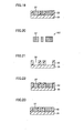
- a metal layer 37 is deposited on recess portion 38 (refer to Fig. 4) of a mold 51 for electroforming as shown in Fig. 5 in the metal layer formation step.
- Metal layer 37 is deposited by electroforming. Electroforming refers to formation of a metal layer on a substrate using a metal solution. Then, grinding or polishing is conducted to attain a desired thickness.
- resist film 33 on substrate 30 is removed by ashing using oxygen plasma or by development after irradiation through an X-ray or UV light. As a result, the configuration shown in Fig. 7 is obtained.
- contact probe 101 as shown in Fig. 8 is obtained. This corresponds to contact probe 101 shown in Fig. 1.
- a contact probe having the plunger unit, spring unit and lead line connection unit formed integrally can be readily fabricated, accommodating the aspects of microminiaturization and complexity of a contact probe. Furthermore, the assembly task is dispensable.
- a probe was fabricated in accordance with the above-described contact probe fabrication method.
- a mold for electroforming was formed by X-ray lithography on a resist applied on a copper plate sputtered with Ti, using a mask corresponding to a planar pattern as shown in Fig. 13. The thickness of all the probes was set to 50 ⁇ m.
- Alloys were prepared all having a nickel preferred orientation of (111) and a nickel average crystal grain size of 50 nm, differing only in the containing amount of manganese, as shown in Table 1. Probes were fabricated based on these alloys.
- a probe was fabricated with the features set similar to those of Examples 1-7 with the exception that manganese is not contained.
- a probe was fabricated with the features set similar to those of Example 4 with the exception that the average crystal grain size was 100 nm.
- a probe was fabricated with the features set similar to those of Example 4 with the exception that the preferred orientation was (200).
- a probe was fabricated with the features set similar to those of Example 5 with the exception that the preferred orientation was (200).
- Fig. 14 the result of X-ray diffraction on a probe fabricated in Example 5 is shown in Fig. 14. It is appreciated from Fig. 14 that the probe had the preferred orientation of (111), the peak intensity ratio of (111) diffraction/(220) diffraction was at least 2, and the peak intensity ratio of (111) diffraction /(220) diffraction was at least 5.
- the crystal grain size was obtained through the Willson scheme and Scherrer scheme based on the diffraction data obtained by XRD. For verification, the crystal grain size was directly confirmed from a TEM (Transmission Electron Microscopy) image.
- the hardness of the material was obtained by universal hardness (HU).
- the universal hardness was evaluated based on ISO Technical Report TR14577 or DIN50359 using a sclerometer by Fischer Instruments K.K.
- the Young's modulus was measured using the aforementioned sclerometer. Also, the Young's modulus was obtained from a load-displacement curve by producing a specimen of H 0.05 mm ⁇ W 0. 3mm ⁇ L 1mm and conducting a bending test. Both measurements were calculated with the Poisson's ratio as 0.3.
- the elastic limit was obtained from the aforementioned bending test result for Young's modulus evaluation.
- a heat resistance test was conducted by measuring the Young's modulus and elastic limit under the state where the sample was maintained at high temperature. The probe was rated as inferior when the Young's modulus or elastic limit was degraded by at least 30%. Any sample fractured during testing was also rated as inferior.
- the heat resistance was evaluated based on the following criteria. ⁇ : Inferiority was not recognized in the measurements under 150°C after being maintained at 150°C for 10 days. ⁇ : Inferiority was recognized in the measurements under 150°C after being maintained at 150°C for two days. ⁇ : The specimen was fractured during the measurement under 100°C after being maintained at 100°C for ten hours.
- Example 1 Concentration wt% Preferred Orientation Average Crystal Grain Size (nm) Hardness (HU) (N/mm 2 ) Young's Modulus (Gpa) Elastic Limit (Mpa) Heat Resistance Example 1 0.005 (111) 50 5800 200 at least 1300 ⁇ Example 2 0.01 (111) 50 5800 210 at least 1300 ⁇ Example 3 0.05 (111) 50 5900 210 at least 1300 ⁇ Example 4 0.1 (111) 50 5850 220 at least 1300 ⁇ Example 5 0.15 (111) 50 5800 225 at least 1300 ⁇ Example 6 0.3 (111) 50 5600 225 1000 ⁇ Example 7 0.4 (111) 50 5450 230 800 ⁇ Comparative Example 1 0 (111) 50 6000 220 at least 1300 ⁇ Comparative Example 2 0.1 (111) 100 4700 200 1100 ⁇ Comparative Example 3 0.1 (200) 50 5050 175
- a probe was fabricated with the features set similar to those of Example 4 with the exception that the average crystal grain size of nickel in the nickel-manganese alloy was set to 30 nm and 70 nm, respectively.
- Example 4 The evaluation results of the obtained probes are shown in Table 2, together with the results of Example 4 and Comparative Example 2.
- All probes were fabricated with 0.1% by weight as the manganese concentration and 50 nm as the average crystal grain size of nickel. Only the concentration of carbon in the nickel-manganese alloy was altered by adjusting the amount of butynediol that is an additive.
- Example 10 0.1 0 50 5800 220 at least 1300 ⁇
- Example 11 0.1 0.001 50 6000 210 at least 1300 ⁇
- Example 12 0.1 0.01 50 6300 230 at least 1300 ⁇
- Example 13 0.1 0.02 50 6600 225 1150 ⁇
- Example 14 0.1 0.03 50 7000 230 700 ⁇
- a contact probe superior in the required characteristics such as elasticity, hardness and the like as well as heat resistance can be provided.
- a contact probe 102 according to a second embodiment of the present invention is shown in Fig. 15.
- Contact probe 102 includes a plunger unit 1 to be brought into contact with an object to be tested, a spring unit 2 supporting plunger unit 1, and a lead line connection unit 3 fixed at the tester side, all formed integrally by a cobalt-tungsten alloy.
- Contact probe 102 is configured with the planar pattern shown in Fig. 13, having a predetermined thickness.
- a resist film 33 is formed on the surface of a substrate 29 having conductivity.
- a metal substrate such as of SUS, Cu, Al, and the like can be used for substrate 29.
- a Si substrate, a glass substrate, and the like can be used instead of substrate 29.
- the metal of Ti, Al, Cu, or a combination thereof is sputtered in advance on the top surface of the Si substrate, glass substrate, and the like to form an underlying conductive layer at the surface.
- an X-ray 35 is directed onto the surface of resist film 33 through mask 34.
- the method of X-ray lithography is employed.
- the method of UV lithography using UV (ultraviolet ray) instead of an X-ray may be employed.
- the resist of exposure portion 36 is removed after development.
- a mold for electroforming 52 with a recess 38 is formed, as shown in Fig. 17.
- electroforming is conducted to fill recess 38 with a metal layer 37 of a cobalt-tungsten alloy.
- This electroforming step can be conducted with a metal-plating solution having cobalt sulfate, sodium tungstate, sodium gluconate, citric acid and other additives mixed appropriately.
- the top surface is ground or polished to be arranged to the desired thickness, as shown in Fig. 19.
- Resist film 33 remaining on substrate 29 is removed by ashing or by development after re-irradiation.
- Substrate 29 is removed by etching or the like.
- a unitary contact probe 102 can be obtained by taking out metal layer 37 alone as shown in Fig. 20. Removal of substrate 29 can be effected by both wet etching and dry etching.
- the hardness of the contact probe fabricated as described above was measured using a Micro-Vickers hardness tester.
- the general contact probe made from nickel or cobalt exhibits the hardness of 600 Hv at most whereas the contact probe of the present invention exhibits an appreciably high hardness of 720 Hv.
- the contact probe was subjected to an abrasion test for 10000 times by being urged against an aluminum plate for scribing. The amount of abrasion at the contact with the aluminum plate was measured. The abrasion amount was 19% the abrasion amount of a nickel contact probe.
- a contact probe is fabricated according to a fabrication method similar to that of the second embodiment, provided that, in the electroforming step of Fig. 18, recess 38 is filled with a metal layer of cobalt-molybdenum alloy instead of metal layer 37 formed of cobalt-tungsten alloy.
- This electroforming step can be conducted with a metal-plating solution having cobalt sulfate, sodium molybdate, citric acid and other additives mixed appropriately.
- a contact probe of a configuration as shown in Fig. 15 was formed with a cobalt-molybdenum alloy, likewise the second embodiment.
- the contact probe fabricated as described above was measured using a Micro-Vickers hardness tester, and exhibited the hardness of 700 Hv.
- the contact probe was subjected to an abrasion test similar to that of the second embodiment.
- the measured amount of abrasion was 14% the abrasion amount of a nickel contact probe.
- a contact probe was fabricated in accordance with the fabrication method of the second embodiment with the electroforming condition altered.
- the percentage content of tungsten in the cobalt-tungsten alloy was increased. It was confirmed that a crack was generated in the contact probe when the percentage content of tungsten exceeds 25% by weight.
- Spring unit 2 cannot function as a spring. Therefore, it is desirable that the percentage content of tungsten is greater than 0% by weight and not more than 25% by weight.
- a probe was fabricated in accordance with the fabrication method of the third embodiment with the electroforming condition altered.
- the amount of molybdenum in the cobalt-molybdenum alloy was increased. It was confirmed that a crack was generated in the contact probe when the content of molybdenum exceeds 18% by weight.
- Spring unit 2 could not function as a spring. Therefore, it is desirable that the percentage content of molybdenum is greater than 0% by weight and not more than 18% by weight.
- Two nickel contact probes were fabricated in accordance with the fabrication method of the second embodiment. These contact probes exhibited the measurement of 550 Hv in hardness. One of these contact probes was coated with a 0.5 ⁇ m-thick film of cobalt-molybdenum alloy on its surface. An abrasion test similar to that of the second embodiment was conducted on the contact probe with the coat film and the contact probe without the coat film, and the amount of abrasion was measured. The amount of abrasion of the contact probe with the coat film was 35% the abrasion amount of the contact probe without the coat film. It is therefore appreciated that formation of a cobalt-molybdenum alloy film on the surface serves to increase the abrasion resistance.
- a similar effect can be achieved even if the coat film is of cobalt-tungsten alloy.
- the metal used for the interior may be cobalt, copper, and the like in addition to nickel.
- a fabrication method of a contact probe according to a seventh embodiment of the present invention will be described with reference to Figs. 9-11, Figs. 21-23, and Fig. 20.
- a resin mold 42 is formed by injection molding or the like using a die 41 having a convex configuration of a contact probe.
- resin mold 42 with a concave configuration corresponding to that of a contact probe is obtained, as shown in Fig. 10.
- Resin mold 42 is subjected to grinding to have the recess portion pierced.
- a resin pattern frame 43 as shown in Fig. 11 is obtained.
- a substrate 29 similar to that used in the second embodiment is prepared, and resin pattern frame 43 is attached thereon, as shown in Fig. 21.
- electroforming is conducted to fill recess 38 with a metal layer 37 of cobalt-tungsten alloy or cobalt-molybdenum alloy. Then, the top surface is ground or polished to be arranged to a predetermined thickness, as shown in Fig. 23.
- Resin pattern frame 43 remaining on substrate 29 is removed by ashing or by development after re-irradiation.
- Substrate 29 is removed by etching or the like. The removal of substrate 29 can be carried out through both wet etching and dry etching. As a result, contact probe 102 shown in Fig. 20 is obtained by taking out only metal layer 37.
- a contact probe of high abrasion resistance can be obtained by employing cobalt-tungsten alloy or cobalt-molybdenum alloy as the material.
- the difference in the percentage content between the plane of initiating electroforming and the plane of ending electroforming is preferably within 25% of the percentage content at the plane of ending electroforming.
- a contact probe is fabricated according to a fabrication method similar to that of the second embodiment, provided that, in the electroforming step of Fig. 18, recess 38 is filled with a metal layer of nickel-molybdenum alloy instead of metal layer 37 formed of cobalt-tungsten alloy.
- This electroforming step can be conducted with a metal-plating solution having nickel sulfate, sodium molybdate, sodium gluconate, citric acid and other additives mixed appropriately.
- a contact probe of a configuration as shown in Fig. 15 was formed with a nickel-molybdenum alloy.
- the contact probe fabricated as described above was measured using a Micro-Vickers hardness tester, and exhibited the hardness of 700 Hv.
- the general contact probe made from nickel or cobalt exhibits the hardness of 600 Hv whereas the contact probe of the present embodiment exhibits a higher hardness.
- the contact probe was subjected to an abrasion test similar to that of the second embodiment, and the abrasion amount was measured.
- the abrasion amount was 20% the abrasion amount of a nickel contact probe.
- a contact probe was fabricated in accordance with the above fabrication method with the electroforming condition altered.
- the percentage content of molybdenum in the nickel-molybdenum alloy was increased. It was confirmed that a crack was generated in the contact probe when the content of molybdenum exceeds 25% by weight, and spring unit 2 cannot function as a spring. Therefore, it is desirable that the percentage content of molybdenum is greater than 0% by weight and not more than 25% by weight.
- a contact probe is fabricated according to a fabrication method similar to that of the seventh embodiment, provided that, in the electroforming step of Fig. 22, recess 38 is filled with a metal layer of nickel-molybdenum alloy instead of metal layer 37 formed of cobalt-tungsten alloy or cobalt-nickel-molybdenum alloy.
- a contact probe of a configuration as shown in Fig. 15 was formed with a nickel-molybdenum alloy.
- a contact probe fabricated as described above offers advantages similar to those of the eighth embodiment.
- a contact probe is coated with a 0.5 ⁇ m-thick film of nickel-molybdenum alloy on its surface.
- An abrasion test similar to that of the second embodiment was conducted on the contact probe with the coat film and the contact probe without the coat film, and the amount of abrasion was measured.
- the amount of abrasion of the contact probe with the coat film was 38% the abrasion amount of the contact probe without the coat film. It is therefore appreciated that formation of a nickel-molybdenum alloy coat film on the surface serves to increase the abrasion resistance.
- the metal used for the interior may be cobalt, copper, and the like in addition to nickel.
- a contact probe of nickel-molybdenum alloy containing 20% by weight molybdenum was fabricated in accordance with the fabrication method of the eighth embodiment.
- the electrical resistance of this contact probe was measured.
- the electrical resistance of this contact probe was 3.5 ⁇ , which is approximately 7 times that of a nickel contact probe.
- This contact probe made from nickel-molybdenum alloy was subjected to a heat treatment of 300°C, whereby the metal crystal of the nickel-molybdenum alloy was partially rendered into ordered alloy. It is found that the electrical resistance is lowered to 0.6 ⁇ , which is substantially equal to that of a nickel contact probe.
- the hardness which was 720 Hv in Vickers hardness prior to the heat treatment is increased to 780 Hv.
- the present embodiment is extremely preferable in that the hardness of the contact probe is maintained at least 600 Hv while the electrical resistance is suppressed to a level equal to that of a nickel contact probe.
- the difference in the percentage content between the plane of initiating electroforming and the plane of ending electroforming is preferably within 25% the percentage content at the plane of ending electroforming.
- the present invention is applicable to a contact probe for use to electrically test a semiconductor IC chip, a liquid crystal display, and the like.
Landscapes
- Chemical & Material Sciences (AREA)
- Engineering & Computer Science (AREA)
- Materials Engineering (AREA)
- Metallurgy (AREA)
- Organic Chemistry (AREA)
- Physics & Mathematics (AREA)
- General Physics & Mathematics (AREA)
- Mechanical Engineering (AREA)
- Chemical Kinetics & Catalysis (AREA)
- Electrochemistry (AREA)
- Measuring Leads Or Probes (AREA)
- Testing Or Measuring Of Semiconductors Or The Like (AREA)
Abstract
Description
○ : Inferiority was not recognized in the measurements under 150°C after being maintained at 150°C for 10 days.
Δ : Inferiority was recognized in the measurements under 150°C after being maintained at 150°C for two days.
× : The specimen was fractured during the measurement under 100°C after being maintained at 100°C for ten hours.
| Mn Concentration wt% | Preferred Orientation | Average Crystal Grain Size (nm) | Hardness (HU) (N/mm2) | Young's Modulus (Gpa) | Elastic Limit (Mpa) | Heat Resistance | |
| Example 1 | 0.005 | (111) | 50 | 5800 | 200 | at least 1300 | Δ |
| Example 2 | 0.01 | (111) | 50 | 5800 | 210 | at least 1300 | ○ |
| Example 3 | 0.05 | (111) | 50 | 5900 | 210 | at least 1300 | ○ |
| Example 4 | 0.1 | (111) | 50 | 5850 | 220 | at least 1300 | ○ |
| Example 5 | 0.15 | (111) | 50 | 5800 | 225 | at least 1300 | ○ |
| Example 6 | 0.3 | (111) | 50 | 5600 | 225 | 1000 | ○ |
| Example 7 | 0.4 | (111) | 50 | 5450 | 230 | 800 | ○ |
| Comparative Example 1 | 0 | (111) | 50 | 6000 | 220 | at least 1300 | × |
| Comparative Example 2 | 0.1 | (111) | 100 | 4700 | 200 | 1100 | ○ |
| Comparative Example 3 | 0.1 | (200) | 50 | 5050 | 175 | 700 | ○ |
| Comparative Example 4 | 0.15 | (200) | 50 | 4500 | 170 | 750 | ○ |
| Mn Concentration wt% | Preferred Orientation | Average Crystal Grain Size (nm) | Hardness (HU) (N/mm2) | Young's Modulus (Gpa) | Elastic Limit (Mpa) | Heat Resistance | |
| Example 8 | 0.1 | (111) | 30 | 5900 | 220 | at least 1300 | ○ |
| Example 4 | 0.1 | (111) | 50 | 5800 | 220 | at least 1300 | ○ |
| Example 9 | 0.1 | (111) | 70 | 5150 | 200 | 1150 | ○ |
| Comparative Example 2 | 0.1 | (111) | 100 | 4700 | 200 | 1100 | ○ |
| Mn Concentration wt% | C Concentration wt% | Average Crystal Grain Size (nm) | Hardness (HU) (N/mm2) | Young's Modulus (Gpa) | Elastic Limit (MPa) | Heat Resistance | |
| Example 10 | 0.1 | 0 | 50 | 5800 | 220 | at least 1300 | ○ |
| Example 11 | 0.1 | 0.001 | 50 | 6000 | 210 | at least 1300 | ○ |
| Example 12 | 0.1 | 0.01 | 50 | 6300 | 230 | at least 1300 | ○ |
| Example 13 | 0.1 | 0.02 | 50 | 6600 | 225 | 1150 | ○ |
| Example 14 | 0.1 | 0.03 | 50 | 7000 | 230 | 700 | ○ |
Claims (15)
- A contact probe fabricated by forming a resin mold on a substrate having conductivity, and filling a cavity of said resin mold with metal through electroforming, wherein said metal is a nickel-manganese alloy, and an average crystal grain size of nickel is not more than 70 nm, and a preferred orientation of a nickel crystal by X-ray diffraction is (111) towards a deposition direction of electroforming.
- The contact probe according to claim 1, wherein said nickel has an average crystal grain size of not more than 50 nm.
- The contact probe according to claim 1, wherein said nickel-manganese alloy contains at least 0.01% by weight and less than 0.3% by weight manganese.
- The contact probe according to claim 1, wherein said nickel-manganese alloy contains carbon.
- The contact probe according to claim 4, wherein said nickel-manganese alloy contains not more than 0.02% by weight carbon.
- A contact probe fabricated by forming a resin mold with a cavity on a substrate having conductivity, and filling said cavity with metal through electroforming, wherein said metal is an alloy for a probe selected from the group consisting of a cobalt-tungsten alloy, cobalt-molybdenum alloy, and nickel-molybdenum alloy.
- The contact probe according to claim 6, wherein said alloy of the probe is a cobalt-tungsten alloy, and a percentage content of tungsten is greater than 0% by weight and 25% by weight at most.
- The contact probe according to claim 6, wherein said alloy of the probe is a cobalt-tungsten alloy, and a difference of the tungsten content of a portion formed by electroforming between an electroforming initiating plane and an electroforming ending plane is within 25% of said content at said ending plane.
- The contact probe according to claim 6, wherein said alloy of the probe is a cobalt-molybdenum alloy, and a percentage content of molybdenum is greater than 0% by weight and 18% by weight at most.
- The contact probe according to claim 6, wherein said alloy of the probe is a cobalt-molybdenum tungsten alloy, and a difference of the molybdenum content of a portion formed by said electroforming between an electroforming initiating plane and an electroforming ending plane is within 25% of said content at said ending plane.
- The contact probe according to claim 6, wherein said alloy of the probe is a nickel-molybdenum alloy, and a percentage content of molybdenum is greater than 0% by weight and 25% by weight at most.
- The contact probe according to claim 6, wherein said alloy of the probe is a nickel-molybdenum tungsten alloy, and a difference of the molybdenum content of a portion formed by said electroforming between an electroforming initiating plane and a an electroforming ending plane is within 25% of said content at said ending plane.
- The contact probe according to claim 6, wherein said alloy of the probe is a nickel-molybdenum alloy, and at least a portion of a metal crystal of said nickel-molybdenum alloy is rendered into ordered alloy by heat treatment.
- A contact probe fabricated by forming a resin mold with a cavity on a substrate having conductivity, and filling said cavity with metal through electroforming, wherein a coat film of at least any alloy selected from the group consisting of a cobalt-tungsten alloy, cobalt-molybdenum alloy and nickel-molybdenum alloy is applied at a surface.
- The contact probe according to claim 14, wherein said metal includes a material selected from the group consisting of nickel, cobalt and copper.
Applications Claiming Priority (5)
| Application Number | Priority Date | Filing Date | Title |
|---|---|---|---|
| JP2001115312 | 2001-04-13 | ||
| JP2001115312 | 2001-04-13 | ||
| JP2001372542 | 2001-12-06 | ||
| JP2001372542 | 2001-12-06 | ||
| PCT/JP2002/003585 WO2002084306A1 (en) | 2001-04-13 | 2002-04-10 | Contact probe |
Publications (3)
| Publication Number | Publication Date |
|---|---|
| EP1387174A1 true EP1387174A1 (en) | 2004-02-04 |
| EP1387174A4 EP1387174A4 (en) | 2005-09-28 |
| EP1387174B1 EP1387174B1 (en) | 2010-05-19 |
Family
ID=26613557
Family Applications (1)
| Application Number | Title | Priority Date | Filing Date |
|---|---|---|---|
| EP02718523A Expired - Lifetime EP1387174B1 (en) | 2001-04-13 | 2002-04-10 | Contact probe |
Country Status (8)
| Country | Link |
|---|---|
| US (1) | US7190179B2 (en) |
| EP (1) | EP1387174B1 (en) |
| JP (1) | JPWO2002084306A1 (en) |
| KR (1) | KR100594074B1 (en) |
| CN (2) | CN1228638C (en) |
| DE (1) | DE60236426D1 (en) |
| TW (1) | TWI276804B (en) |
| WO (1) | WO2002084306A1 (en) |
Cited By (3)
| Publication number | Priority date | Publication date | Assignee | Title |
|---|---|---|---|---|
| EP1685415A4 (en) * | 2003-10-24 | 2011-07-20 | Wentworth Lab Inc | METHOD FOR FORMING ELECTRIC MICROCONTACTS PHOTODEFINIS |
| EP2980278A4 (en) * | 2013-08-02 | 2016-04-13 | Omron Tateisi Electronics Co | ELECTROFORMED COMPONENT AND METHOD FOR MANUFACTURING THE SAME |
| DE102019123205B4 (en) | 2018-09-28 | 2023-01-19 | Advantest Corporation | Pore chip housing and small particle measurement system |
Families Citing this family (38)
| Publication number | Priority date | Publication date | Assignee | Title |
|---|---|---|---|---|
| JP3714262B2 (en) * | 2002-02-20 | 2005-11-09 | 住友電気工業株式会社 | Fine electroforming mold and its manufacturing method |
| KR100443999B1 (en) | 2003-02-28 | 2004-08-21 | 주식회사 파이컴 | Interconnector for Printed Circuit Board, method thereby and interconnector assembly having it |
| KR100573089B1 (en) | 2003-03-17 | 2006-04-24 | 주식회사 파이컴 | Probe and its manufacturing method |
| JP3745744B2 (en) * | 2003-04-16 | 2006-02-15 | 住友電気工業株式会社 | Method for producing metal structure and metal structure produced by the method |
| JP2005127952A (en) * | 2003-10-27 | 2005-05-19 | Sumitomo Electric Ind Ltd | Contact probe and manufacturing method thereof |
| KR100653636B1 (en) * | 2005-08-03 | 2006-12-05 | 주식회사 파이컴 | Vertical probe, manufacturing method thereof and bonding method of probe |
| KR200411355Y1 (en) * | 2005-12-26 | 2006-03-15 | 송광석 | Probe Card for Semiconductor Inspection |
| KR100852514B1 (en) * | 2006-07-31 | 2008-08-18 | 한국과학기술연구원 | Vertical probes for semiconductor inspection, probe cards having the probes and a method of manufacturing the same |
| US7687304B2 (en) * | 2006-11-29 | 2010-03-30 | Innovative Micro Technology | Current-driven device using NiMn alloy and method of manufacture |
| JP2009002845A (en) * | 2007-06-22 | 2009-01-08 | Micronics Japan Co Ltd | Contact and connection device |
| US20090144970A1 (en) * | 2007-12-06 | 2009-06-11 | Winmems Technologies Holdings Co., Ltd. | Fabricating an array of mems parts on a substrate |
| US7811849B2 (en) * | 2008-01-30 | 2010-10-12 | Winmems Technologies Co., Ltd. | Placing a MEMS part on an application platform using a guide mask |
| US8089294B2 (en) * | 2008-08-05 | 2012-01-03 | WinMENS Technologies Co., Ltd. | MEMS probe fabrication on a reusable substrate for probe card application |
| US7737714B2 (en) * | 2008-11-05 | 2010-06-15 | Winmems Technologies Holdings Co., Ltd. | Probe assembly arrangement |
| US7928751B2 (en) * | 2009-02-18 | 2011-04-19 | Winmems Technologies Holdings Co., Ltd. | MEMS interconnection pins fabrication on a reusable substrate for probe card application |
| TWI429789B (en) * | 2010-03-11 | 2014-03-11 | Omron Tateisi Electronics Co | Composition for making contact, contact made therewith, connector, and method for producing the composition for making contact |
| TW201135239A (en) * | 2010-04-02 | 2011-10-16 | Pleader Yamaichi Co Ltd | High-frequency vertical elastic probe structure |
| JP5798315B2 (en) * | 2010-11-19 | 2015-10-21 | 株式会社神戸製鋼所 | Contact probe pin |
| JP5839798B2 (en) * | 2010-12-17 | 2016-01-06 | 株式会社オプトニクス精密 | Probe card |
| TWI458985B (en) * | 2011-02-23 | 2014-11-01 | King Yuan Electronics Co Ltd | A hard and wear-resisting probe and manufacturing method thereof |
| US10006938B2 (en) * | 2012-01-04 | 2018-06-26 | Formfactor, Inc. | Probes with programmable motion |
| CN104254781B (en) * | 2012-03-07 | 2021-10-15 | 爱德万测试公司 | Transfer Electron Probe Assembly to Space Transformer |
| US9494618B2 (en) * | 2012-12-26 | 2016-11-15 | Translarity, Inc. | Designed asperity contactors, including nanospikes, for semiconductor test using a package, and associated systems and methods |
| JP6487813B2 (en) * | 2015-09-01 | 2019-03-20 | 住友電気工業株式会社 | Nickel tungsten alloy and contact probe |
| JP1558740S (en) * | 2015-11-12 | 2016-09-12 | ||
| JP1558199S (en) * | 2015-11-12 | 2016-09-12 | ||
| JP1558200S (en) * | 2015-11-12 | 2016-09-12 | ||
| US10168357B2 (en) * | 2015-12-21 | 2019-01-01 | Intel Corporation | Coated probe tips for plunger pins of an integrated circuit package test system |
| CN105807213A (en) * | 2016-05-30 | 2016-07-27 | 青岛港湾职业技术学院 | Testing device for flat lead chip |
| SG11201911857UA (en) | 2017-06-14 | 2020-01-30 | Nhk Spring Co Ltd | Conductive contactor unit |
| JP7191078B2 (en) * | 2017-07-12 | 2022-12-16 | ヒル・アンド・ミユラー・ゲゼルシヤフト・ミツト・ベシユレンクテル・ハフツング | Materials with low interfacial contact resistance, uses thereof, and methods of making same |
| CN108593980A (en) * | 2018-04-18 | 2018-09-28 | 强半导体(苏州)有限公司 | A kind of manufacturing method of contact probe, measuring head and contact probe |
| CN110205660B (en) * | 2019-06-24 | 2020-11-03 | 东莞市连威电子有限公司 | Manual control electroplating method for transverse section of wire needle jig |
| KR102795790B1 (en) * | 2021-06-28 | 2025-04-15 | 백정균 | probe member for test, manufacturing method thereof |
| JP2024058296A (en) | 2022-10-14 | 2024-04-25 | 株式会社アドバンテスト | Pore Devices and Particle Measurement Systems |
| JP2024081540A (en) | 2022-12-06 | 2024-06-18 | 株式会社アドバンテスト | Pore Tips and Particle Measurement Systems |
| IT202300008097A1 (en) * | 2023-04-26 | 2024-10-26 | Technoprobe Spa | Measuring head with contact probes having improved deformation properties |
| JP2025114004A (en) * | 2024-01-23 | 2025-08-04 | 松田産業株式会社 | Molybdenum-containing palladium-nickel alloy coating, method for producing the same, and molybdenum-containing palladium-nickel alloy plating solution |
Family Cites Families (32)
| Publication number | Priority date | Publication date | Assignee | Title |
|---|---|---|---|---|
| US4774462A (en) * | 1984-06-11 | 1988-09-27 | Black Thomas J | Automatic test system |
| EP0256541A3 (en) * | 1986-08-19 | 1990-03-14 | Feinmetall Gesellschaft mit beschrÀ¤nkter Haftung | Contacting device |
| DE8711110U1 (en) | 1986-08-19 | 1987-12-17 | Feinmetall Gmbh, 7033 Herrenberg | Contacting device |
| DE3643305A1 (en) | 1986-12-18 | 1988-06-30 | Feinmetall Gmbh | CONTACT ELEMENT FOR TEST ADAPTER |
| US5148810A (en) | 1990-02-12 | 1992-09-22 | Acuson Corporation | Variable origin-variable angle acoustic scanning method and apparatus |
| US5015947A (en) * | 1990-03-19 | 1991-05-14 | Tektronix, Inc. | Low capacitance probe tip |
| DE4029829A1 (en) | 1990-09-20 | 1992-04-02 | Dornier Medizintechnik | THREE-DIMENSIONAL REPRESENTATION OF ULTRASONIC IMAGES |
| EP0629867B1 (en) * | 1993-06-16 | 1999-01-27 | Nitto Denko Corporation | Probe structure |
| JPH0727789A (en) | 1993-07-09 | 1995-01-31 | Nitto Denko Corp | Circuit wiring board and manufacturing method thereof |
| US6835898B2 (en) * | 1993-11-16 | 2004-12-28 | Formfactor, Inc. | Electrical contact structures formed by configuring a flexible wire to have a springable shape and overcoating the wire with at least one layer of a resilient conductive material, methods of mounting the contact structures to electronic components, and applications for employing the contact structures |
| US5513430A (en) * | 1994-08-19 | 1996-05-07 | Motorola, Inc. | Method for manufacturing a probe |
| KR970707444A (en) * | 1994-10-28 | 1997-12-01 | 야마모토 히데키 | PROBE STRUCTURE |
| JP2706432B2 (en) | 1995-07-24 | 1998-01-28 | 日東工業株式会社 | Fixing belt and fixing device for electrophotographic apparatus |
| JPH09119945A (en) | 1995-10-24 | 1997-05-06 | S I I Micro Parts:Kk | Contact terminal for contact probe pin |
| US5667410A (en) * | 1995-11-21 | 1997-09-16 | Everett Charles Technologies, Inc. | One-piece compliant probe |
| JPH09279365A (en) | 1996-04-11 | 1997-10-28 | Mitsubishi Materials Corp | Method for manufacturing microstructured parts |
| JPH10303258A (en) | 1997-04-22 | 1998-11-13 | Sumitomo Electric Ind Ltd | Inspection equipment for electronic and electric circuits |
| JPH1144708A (en) * | 1997-07-24 | 1999-02-16 | Mitsubishi Materials Corp | Contact probe and manufacturing method thereof |
| JP3822722B2 (en) | 1997-08-12 | 2006-09-20 | ジェネシス・テクノロジー株式会社 | Contact probe, method of manufacturing the same, and probe device including the contact probe |
| JP3458684B2 (en) * | 1997-11-28 | 2003-10-20 | 三菱マテリアル株式会社 | Contact probe |
| JPH11191453A (en) | 1997-12-25 | 1999-07-13 | Oputonikusu Seimitsu:Kk | Terminal board and method of manufacturing the same |
| JPH11269587A (en) | 1998-03-24 | 1999-10-05 | Toru Yamazaki | Alloy by electrolytic deposition, and micro-arry connector using the same |
| JP3446607B2 (en) | 1998-05-18 | 2003-09-16 | 三菱マテリアル株式会社 | Method of manufacturing contact pin and contact probe |
| JP3281601B2 (en) | 1998-05-26 | 2002-05-13 | 武田産業株式会社 | Method of manufacturing probe needle and spring for spring probe |
| SG75186A1 (en) | 1998-11-30 | 2000-09-19 | Advantest Corp | Method for producing contact structures |
| US5989994A (en) * | 1998-12-29 | 1999-11-23 | Advantest Corp. | Method for producing contact structures |
| JP2001013166A (en) | 1999-06-28 | 2001-01-19 | Toshiba Corp | Probe structure for semiconductor device evaluation and method of manufacturing the same |
| NL1012695C2 (en) * | 1999-07-23 | 2001-01-24 | Berg Electronics Mfg | Contact element, method of manufacturing it, and connector comprising the same. |
| JP2001174482A (en) | 1999-12-21 | 2001-06-29 | Toshiba Corp | Contact needle for electrical property evaluation, probe structure, probe card, and method of manufacturing contact needle for electrical property evaluation |
| JP2001342591A (en) * | 2000-03-27 | 2001-12-14 | Takayasu Mochizuki | High strength alloy and manufacturing method, and coated metal with high strength alloy and micro structural body using it |
| JP3773396B2 (en) | 2000-06-01 | 2006-05-10 | 住友電気工業株式会社 | Contact probe and manufacturing method thereof |
| KR100576898B1 (en) | 2001-01-29 | 2006-05-03 | 스미토모덴키고교가부시키가이샤 | Contact probe, method of manufacturing the contact probe, and device and method for inspection |
-
2002
- 2002-04-10 US US10/472,571 patent/US7190179B2/en not_active Expired - Fee Related
- 2002-04-10 KR KR1020037013278A patent/KR100594074B1/en not_active Expired - Fee Related
- 2002-04-10 CN CNB028102886A patent/CN1228638C/en not_active Expired - Fee Related
- 2002-04-10 WO PCT/JP2002/003585 patent/WO2002084306A1/en not_active Ceased
- 2002-04-10 DE DE60236426T patent/DE60236426D1/en not_active Expired - Lifetime
- 2002-04-10 CN CNB2005100764016A patent/CN100339715C/en not_active Expired - Fee Related
- 2002-04-10 EP EP02718523A patent/EP1387174B1/en not_active Expired - Lifetime
- 2002-04-10 JP JP2002582008A patent/JPWO2002084306A1/en active Pending
- 2002-04-11 TW TW091107359A patent/TWI276804B/en not_active IP Right Cessation
Cited By (3)
| Publication number | Priority date | Publication date | Assignee | Title |
|---|---|---|---|---|
| EP1685415A4 (en) * | 2003-10-24 | 2011-07-20 | Wentworth Lab Inc | METHOD FOR FORMING ELECTRIC MICROCONTACTS PHOTODEFINIS |
| EP2980278A4 (en) * | 2013-08-02 | 2016-04-13 | Omron Tateisi Electronics Co | ELECTROFORMED COMPONENT AND METHOD FOR MANUFACTURING THE SAME |
| DE102019123205B4 (en) | 2018-09-28 | 2023-01-19 | Advantest Corporation | Pore chip housing and small particle measurement system |
Also Published As
| Publication number | Publication date |
|---|---|
| US20040104739A1 (en) | 2004-06-03 |
| DE60236426D1 (en) | 2010-07-01 |
| CN1696709A (en) | 2005-11-16 |
| EP1387174B1 (en) | 2010-05-19 |
| CN1228638C (en) | 2005-11-23 |
| EP1387174A4 (en) | 2005-09-28 |
| US7190179B2 (en) | 2007-03-13 |
| TWI276804B (en) | 2007-03-21 |
| KR20030093307A (en) | 2003-12-06 |
| CN1511260A (en) | 2004-07-07 |
| CN100339715C (en) | 2007-09-26 |
| WO2002084306A1 (en) | 2002-10-24 |
| KR100594074B1 (en) | 2006-06-30 |
| JPWO2002084306A1 (en) | 2004-08-05 |
Similar Documents
| Publication | Publication Date | Title |
|---|---|---|
| EP1387174B1 (en) | Contact probe | |
| KR101453474B1 (en) | Electrical Test Probe | |
| US7586321B2 (en) | Electrical test probe and electrical test probe assembly | |
| US9116173B2 (en) | Contact probe having carbon film on surface thereof | |
| US20020153913A1 (en) | Probe for the probe card | |
| US8410367B2 (en) | Electric contact member | |
| KR101153288B1 (en) | Probe for electrical test, electrical connecting apparatus using the same, and method for manufacturing probe | |
| US8159248B2 (en) | Interposer structures and methods of manufacturing the same | |
| US20080280542A1 (en) | Cleaning apparatus for a probe | |
| EP2762898A1 (en) | Method for manufacturing contact probe | |
| JP2006064511A (en) | Metal structure | |
| KR101034828B1 (en) | Metal structure and method of manufacturing the same | |
| JP2001116765A (en) | Probe card pin | |
| KR100349614B1 (en) | Miniscale probe and the vertically operating probe card that uses it | |
| Zhou et al. | Usability of silver plating and silver bismuth alloy plating on electrical contacts | |
| KR20250146452A (en) | High wear resistance micro-conductive ball with outermost PtAu alloy thin film | |
| TW202603369A (en) | Tip structure and contact pin | |
| HK1083536A (en) | Contact probe | |
| JP2005300391A (en) | Metal structure and manufacturing method thereof | |
| JP2005008986A (en) | Metal structure and manufacturing method thereof |
Legal Events
| Date | Code | Title | Description |
|---|---|---|---|
| PUAI | Public reference made under article 153(3) epc to a published international application that has entered the european phase |
Free format text: ORIGINAL CODE: 0009012 |
|
| 17P | Request for examination filed |
Effective date: 20031023 |
|
| AK | Designated contracting states |
Kind code of ref document: A1 Designated state(s): AT BE CH CY DE DK ES FI FR GB GR IE IT LI LU MC NL PT SE TR |
|
| A4 | Supplementary search report drawn up and despatched |
Effective date: 20050817 |
|
| 17Q | First examination report despatched |
Effective date: 20071011 |
|
| GRAP | Despatch of communication of intention to grant a patent |
Free format text: ORIGINAL CODE: EPIDOSNIGR1 |
|
| RBV | Designated contracting states (corrected) |
Designated state(s): DE |
|
| GRAS | Grant fee paid |
Free format text: ORIGINAL CODE: EPIDOSNIGR3 |
|
| GRAA | (expected) grant |
Free format text: ORIGINAL CODE: 0009210 |
|
| AK | Designated contracting states |
Kind code of ref document: B1 Designated state(s): DE |
|
| REF | Corresponds to: |
Ref document number: 60236426 Country of ref document: DE Date of ref document: 20100701 Kind code of ref document: P |
|
| PLBE | No opposition filed within time limit |
Free format text: ORIGINAL CODE: 0009261 |
|
| STAA | Information on the status of an ep patent application or granted ep patent |
Free format text: STATUS: NO OPPOSITION FILED WITHIN TIME LIMIT |
|
| 26N | No opposition filed |
Effective date: 20110222 |
|
| REG | Reference to a national code |
Ref country code: DE Ref legal event code: R097 Ref document number: 60236426 Country of ref document: DE Effective date: 20110221 |
|
| PGFP | Annual fee paid to national office [announced via postgrant information from national office to epo] |
Ref country code: DE Payment date: 20140430 Year of fee payment: 13 |
|
| REG | Reference to a national code |
Ref country code: DE Ref legal event code: R119 Ref document number: 60236426 Country of ref document: DE |
|
| PG25 | Lapsed in a contracting state [announced via postgrant information from national office to epo] |
Ref country code: DE Free format text: LAPSE BECAUSE OF NON-PAYMENT OF DUE FEES Effective date: 20151103 |