EP1381054A1 - Organic memory device - Google Patents
Organic memory device Download PDFInfo
- Publication number
- EP1381054A1 EP1381054A1 EP03014548A EP03014548A EP1381054A1 EP 1381054 A1 EP1381054 A1 EP 1381054A1 EP 03014548 A EP03014548 A EP 03014548A EP 03014548 A EP03014548 A EP 03014548A EP 1381054 A1 EP1381054 A1 EP 1381054A1
- Authority
- EP
- European Patent Office
- Prior art keywords
- organic
- electrode lines
- memory
- memory device
- layer
- Prior art date
- Legal status (The legal status is an assumption and is not a legal conclusion. Google has not performed a legal analysis and makes no representation as to the accuracy of the status listed.)
- Granted
Links
- 239000004065 semiconductor Substances 0.000 claims abstract description 39
- 230000004044 response Effects 0.000 claims description 3
- 239000012071 phase Substances 0.000 description 35
- 239000000463 material Substances 0.000 description 23
- 238000000034 method Methods 0.000 description 13
- 239000011368 organic material Substances 0.000 description 10
- 230000007704 transition Effects 0.000 description 10
- 239000002019 doping agent Substances 0.000 description 7
- 239000000758 substrate Substances 0.000 description 7
- 229910052751 metal Inorganic materials 0.000 description 5
- 239000002184 metal Substances 0.000 description 5
- RBTKNAXYKSUFRK-UHFFFAOYSA-N heliogen blue Chemical compound [Cu].[N-]1C2=C(C=CC=C3)C3=C1N=C([N-]1)C3=CC=CC=C3C1=NC([N-]1)=C(C=CC=C3)C3=C1N=C([N-]1)C3=CC=CC=C3C1=N2 RBTKNAXYKSUFRK-UHFFFAOYSA-N 0.000 description 3
- 238000012986 modification Methods 0.000 description 3
- 230000004048 modification Effects 0.000 description 3
- IEQIEDJGQAUEQZ-UHFFFAOYSA-N phthalocyanine Chemical compound N1C(N=C2C3=CC=CC=C3C(N=C3C4=CC=CC=C4C(=N4)N3)=N2)=C(C=CC=C2)C2=C1N=C1C2=CC=CC=C2C4=N1 IEQIEDJGQAUEQZ-UHFFFAOYSA-N 0.000 description 3
- 229920000642 polymer Polymers 0.000 description 3
- 229910052725 zinc Inorganic materials 0.000 description 3
- 239000011701 zinc Substances 0.000 description 3
- HCHKCACWOHOZIP-UHFFFAOYSA-N Zinc Chemical compound [Zn] HCHKCACWOHOZIP-UHFFFAOYSA-N 0.000 description 2
- 230000004075 alteration Effects 0.000 description 2
- 229910052782 aluminium Inorganic materials 0.000 description 2
- XAGFODPZIPBFFR-UHFFFAOYSA-N aluminium Chemical compound [Al] XAGFODPZIPBFFR-UHFFFAOYSA-N 0.000 description 2
- MWPLVEDNUUSJAV-UHFFFAOYSA-N anthracene Chemical compound C1=CC=CC2=CC3=CC=CC=C3C=C21 MWPLVEDNUUSJAV-UHFFFAOYSA-N 0.000 description 2
- 230000001747 exhibiting effect Effects 0.000 description 2
- 239000011521 glass Substances 0.000 description 2
- 239000010931 gold Substances 0.000 description 2
- 239000011159 matrix material Substances 0.000 description 2
- 239000002861 polymer material Substances 0.000 description 2
- 238000006116 polymerization reaction Methods 0.000 description 2
- 239000011734 sodium Substances 0.000 description 2
- -1 zinc phthalocyanine porphyrin Chemical class 0.000 description 2
- 229910001218 Gallium arsenide Inorganic materials 0.000 description 1
- DGAQECJNVWCQMB-PUAWFVPOSA-M Ilexoside XXIX Chemical compound C[C@@H]1CC[C@@]2(CC[C@@]3(C(=CC[C@H]4[C@]3(CC[C@@H]5[C@@]4(CC[C@@H](C5(C)C)OS(=O)(=O)[O-])C)C)[C@@H]2[C@]1(C)O)C)C(=O)O[C@H]6[C@@H]([C@H]([C@@H]([C@H](O6)CO)O)O)O.[Na+] DGAQECJNVWCQMB-PUAWFVPOSA-M 0.000 description 1
- 239000002841 Lewis acid Substances 0.000 description 1
- 229920000265 Polyparaphenylene Polymers 0.000 description 1
- ZLMJMSJWJFRBEC-UHFFFAOYSA-N Potassium Chemical compound [K] ZLMJMSJWJFRBEC-UHFFFAOYSA-N 0.000 description 1
- XBDYBAVJXHJMNQ-UHFFFAOYSA-N Tetrahydroanthracene Natural products C1=CC=C2C=C(CCCC3)C3=CC2=C1 XBDYBAVJXHJMNQ-UHFFFAOYSA-N 0.000 description 1
- 239000002253 acid Substances 0.000 description 1
- 229910052783 alkali metal Inorganic materials 0.000 description 1
- 150000001340 alkali metals Chemical class 0.000 description 1
- 125000005210 alkyl ammonium group Chemical group 0.000 description 1
- 238000013459 approach Methods 0.000 description 1
- 230000015572 biosynthetic process Effects 0.000 description 1
- 229910052797 bismuth Inorganic materials 0.000 description 1
- 238000005266 casting Methods 0.000 description 1
- 239000002131 composite material Substances 0.000 description 1
- 150000001875 compounds Chemical class 0.000 description 1
- 239000000470 constituent Substances 0.000 description 1
- 238000012937 correction Methods 0.000 description 1
- 230000007423 decrease Effects 0.000 description 1
- 230000003247 decreasing effect Effects 0.000 description 1
- 238000000151 deposition Methods 0.000 description 1
- 230000005684 electric field Effects 0.000 description 1
- 230000002349 favourable effect Effects 0.000 description 1
- 230000006870 function Effects 0.000 description 1
- PCHJSUWPFVWCPO-UHFFFAOYSA-N gold Chemical compound [Au] PCHJSUWPFVWCPO-UHFFFAOYSA-N 0.000 description 1
- 229910052737 gold Inorganic materials 0.000 description 1
- 229910052736 halogen Inorganic materials 0.000 description 1
- 150000002367 halogens Chemical class 0.000 description 1
- 125000001072 heteroaryl group Chemical group 0.000 description 1
- AMGQUBHHOARCQH-UHFFFAOYSA-N indium;oxotin Chemical compound [In].[Sn]=O AMGQUBHHOARCQH-UHFFFAOYSA-N 0.000 description 1
- 238000005468 ion implantation Methods 0.000 description 1
- 150000007517 lewis acids Chemical class 0.000 description 1
- 239000007791 liquid phase Substances 0.000 description 1
- 238000002844 melting Methods 0.000 description 1
- 230000008018 melting Effects 0.000 description 1
- 238000001451 molecular beam epitaxy Methods 0.000 description 1
- 238000005232 molecular self-assembly Methods 0.000 description 1
- SLIUAWYAILUBJU-UHFFFAOYSA-N pentacene Chemical compound C1=CC=CC2=CC3=CC4=CC5=CC=CC=C5C=C4C=C3C=C21 SLIUAWYAILUBJU-UHFFFAOYSA-N 0.000 description 1
- 125000002080 perylenyl group Chemical group C1(=CC=C2C=CC=C3C4=CC=CC5=CC=CC(C1=C23)=C45)* 0.000 description 1
- 229920003023 plastic Polymers 0.000 description 1
- 239000004033 plastic Substances 0.000 description 1
- 229920001467 poly(styrenesulfonates) Polymers 0.000 description 1
- 229920001197 polyacetylene Polymers 0.000 description 1
- 229920000767 polyaniline Polymers 0.000 description 1
- 239000005518 polymer electrolyte Substances 0.000 description 1
- 229920000128 polypyrrole Polymers 0.000 description 1
- 229960002796 polystyrene sulfonate Drugs 0.000 description 1
- 239000011970 polystyrene sulfonate Substances 0.000 description 1
- 229920000123 polythiophene Polymers 0.000 description 1
- 229910052700 potassium Inorganic materials 0.000 description 1
- 239000011591 potassium Substances 0.000 description 1
- 230000008569 process Effects 0.000 description 1
- 230000005855 radiation Effects 0.000 description 1
- 238000012827 research and development Methods 0.000 description 1
- 229910052708 sodium Inorganic materials 0.000 description 1
- 238000009987 spinning Methods 0.000 description 1
- 239000000126 substance Substances 0.000 description 1
- BDHFUVZGWQCTTF-UHFFFAOYSA-M sulfonate Chemical compound [O-]S(=O)=O BDHFUVZGWQCTTF-UHFFFAOYSA-M 0.000 description 1
- IFLREYGFSNHWGE-UHFFFAOYSA-N tetracene Chemical compound C1=CC=CC2=CC3=CC4=CC=CC=C4C=C3C=C21 IFLREYGFSNHWGE-UHFFFAOYSA-N 0.000 description 1
- 229910021381 transition metal chloride Inorganic materials 0.000 description 1
- 238000001771 vacuum deposition Methods 0.000 description 1
- 238000007740 vapor deposition Methods 0.000 description 1
- 229920002554 vinyl polymer Polymers 0.000 description 1
Images






Classifications
-
- G—PHYSICS
- G11—INFORMATION STORAGE
- G11C—STATIC STORES
- G11C13/00—Digital stores characterised by the use of storage elements not covered by groups G11C11/00, G11C23/00, or G11C25/00
- G11C13/0002—Digital stores characterised by the use of storage elements not covered by groups G11C11/00, G11C23/00, or G11C25/00 using resistive RAM [RRAM] elements
- G11C13/0009—RRAM elements whose operation depends upon chemical change
- G11C13/0014—RRAM elements whose operation depends upon chemical change comprising cells based on organic memory material
-
- B—PERFORMING OPERATIONS; TRANSPORTING
- B82—NANOTECHNOLOGY
- B82Y—SPECIFIC USES OR APPLICATIONS OF NANOSTRUCTURES; MEASUREMENT OR ANALYSIS OF NANOSTRUCTURES; MANUFACTURE OR TREATMENT OF NANOSTRUCTURES
- B82Y10/00—Nanotechnology for information processing, storage or transmission, e.g. quantum computing or single electron logic
-
- G—PHYSICS
- G11—INFORMATION STORAGE
- G11C—STATIC STORES
- G11C13/00—Digital stores characterised by the use of storage elements not covered by groups G11C11/00, G11C23/00, or G11C25/00
- G11C13/0002—Digital stores characterised by the use of storage elements not covered by groups G11C11/00, G11C23/00, or G11C25/00 using resistive RAM [RRAM] elements
- G11C13/0009—RRAM elements whose operation depends upon chemical change
- G11C13/0014—RRAM elements whose operation depends upon chemical change comprising cells based on organic memory material
- G11C13/0016—RRAM elements whose operation depends upon chemical change comprising cells based on organic memory material comprising polymers
Definitions
- the present invention relates to an organic switching memory device that permits writing and rewriting and in which organic material is employed, and to a memory apparatus or the like having the memory device.
- Examples of conventional memory devices employing organic materials include, for example, a mask ROM (Read Only Memory) that utilizes an organic diode as disclosed by Japanese Patent Kohyo No. 2001-516964. Because the memory device does not permit electrical writing, the use of the memory device is limited to a mask ROM and the memory element cannot therefore be applied to a memory device that is capable of performing electrical writing or rewriting operations.
- a mask ROM Read Only Memory
- examples of other memory devices include the memory device disclosed by Japanese Patent Kokai No. 08-116109.
- the memory device utilizes a material which changes in resistance in accordance with the application of a voltage and retains the resistance value even upon removal of the application voltage.
- a switching element for increasing the capacity of a memory device, a straightforward method has not been proposed in which the characteristics of the organic material are utilized.
- the prior art has therefore been confronted by a problem such that it is difficult to implement a large-capacity organic memory device and a memory apparatus that permits electrical writing or rewriting in a high-performance organic memory device or memory apparatus.
- the problem mentioned above is cited as one example of the problems which the present invention is intended to resolve.
- an organic switching memory device which comprises a plurality of first electrode lines; an organic memory layer formed on the plurality of first electrode lines, the organic memory layer exhibiting a voltage-current hysteresis characteristic; a semiconductor diode layer stacked on the organic memory layer; and a plurality of second electrode lines formed on the semiconductor diode layer, the plurality of second electrode lines being disposed in a direction so as to intersect the plurality of first electrode lines.
- a memory apparatus which comprises a organic switching memory device having a plurality of first electrode lines, an organic memory layer formed on the plurality of first electrode lines, the organic memory layer exhibiting a voltage-current hysteresis characteristic; a semiconductor diode layer stacked on the organic memory layer; and a plurality of second electrode lines formed on the semiconductor diode layer, the plurality of second electrode lines being disposed in a direction so as to intersect the plurality of first electrode lines, a receiver section for receiving an address designation signal, data and a write command signal, the address designation signal designating addresses which correspond to intersecting positions of the plurality of first electrode lines and the plurality of second electrode lines, and a control section which writes the data to the organic switching memory device on the basis of the address designation signal, in response to the write command signal.
- Fig. 1 is a plan view of part of a memory device 10 according to a first embodiment of the present invention
- Fig. 2 is a cross-sectional view of a region that comprises a memory cell portion of the memory device 10 shown in Fig. 1.
- the memory device 10 is constituted by stacking, on a substrate 11, a lower electrode (hereinafter, also referred to as bit lines Bi) 12, a memory layer 14, a semiconductor layer 15, and an upper electrode (hereinafter, also referred to as word lines Wj) 16, in this order.
- bit lines Bi lower electrode
- Wj upper electrode
- the substrate 11 is constituted by alkali-free glass, for example.
- the memory layer 14 is formed by an organic memory material such as zinc phthalocyanine (ZnPc) or zinc phthalocyanine porphyrin, for example.
- the semiconductor layer 15 is a p-n junction organic semiconductor diode in which copper phthalocyanine is used as the p-type material and a perylene derivative is used as the n-type material, for example.
- the p-type organic semiconductor layer is connected to the memory layer 14 and the n-type organic semiconductor layer is connected to the upper electrode 16 described hereinafter.
- a plurality of second electrode lines provided by a metal such as aluminum (Al), that is, stripe-shaped word lines Wj (j 1, 2, . . .n), are arranged on the semiconductor layer 15 so as to be mutually parallel and lie in a direction that sterically intersects bit lines Bi, in a direction orthogonal to bit lines Bi, for example.
- An ohmic contact is formed between the upper electrode (word lines Wj) 16 and the semiconductor layer 15 (n-type organic semiconductor layer).
- the lower electrode (bit lines Bi) 12, the memory layer 14, the semiconductor layer 15 and the upper electrode (word lines Wj) 16 are formed by means of vacuum vapor deposition.
- memory cells C(j,i) are formed in the regions of intersections between the word lines Wj and the bit lines Bi. More particularly, each of the memory cells C(j,i) has a structure in which the word line (Wj) 16, the semiconductor layer (diode junction) 15, the memory layer 14 and the bit line (Bi) 12 are connected in series. Further, the memory cells C(j,i) are arranged in the form of a matrix. As will be described later, the memory cells C(j,i) serve as switching memory composite elements.
- Fig. 3 corresponds to Fig. 1 and shows an electrical equivalent circuit corresponding to a part of the memory device 10.
- the diodes Di corresponds to the diode junction of the semiconductor layer 15 and the resistors R corresponds to the memory layer 14 (Fig. 2).
- Each of the memory cells C(j,i) can be represented as a serial connection of the diode Di and the resistor R.
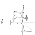
- Fig. 4 shows an example of the current-voltage characteristic (I-V characteristic) of the organic memory material (zinc phthalocyanine: ZnPc) employed for the memory layer 14 .
- Such an organic memory material exhibits a hysteresis loop characteristic. More particularly, when the memory material is in a high-resistance phase state (reset state), the current value increases in accordance with the resistance value of the high-resistance phase region as the voltage applied to the memory material is increased. As the application voltage approaches V w , the current value starts to increase rapidly, and the memory material makes a phase transition to a low resistance phase when the application voltage reaches +V w (V w >0).
- the current value decreases in accordance with the resistance value in the low resistance phase region as the application voltage is decreased from the transition voltage V w .
- the application voltage is reduced further and the application voltage reaches -V E (V E >0)
- the current value increases abruptly and the memory material makes the phase transition to a high resistance phase.
- a memory material may also be used that has an I-V hysteresis characteristic such that current variations have the form of a curve.
- the memory material makes the phase transition to the low resistance phase by an application of a voltage that is equal to or greater than +V w (V w >0), and makes the phase transition to the high resistance phase by an application of a voltage that is equal to or less than -V E (V E >0). Therefore, writing of binary data can be performed by varying the voltage which is applied to the memory cells through the use of the I-V characteristic of the memory material. Furthermore, as shown in Fig. 4, the data thus written can be read out by applying a voltage V R that lies between -V E and +V w to the memory device or cell to detect the difference in the electric current values (that is, for example, I0 and I1).
- Fig. 5 shows the configuration of a memory apparatus 20 that uses a memory device 10.
- the memory apparatus 20 comprises a memory device 10, which includes the above-mentioned matrix memory array, a controller 21, an address selection circuit 23, and a write/read control circuit (hereinafter, simply referred to as a 'write/read circuit') 24.
- Address designation signals are supplied from the controller 21 to the address selection circuit 23, and a write control signal or a read control signal is supplied from the controller 21 to the write/read circuit 24.
- the address selection circuit 23 may include an address register (not shown).
- the write/read circuit 24 may include a write register/read register (not shown).
- the controller 21 performs writing to the memory device 10 on the basis of external data and control signals or on the basis of control signals and data which are generated internally, and outputs data read out from the memory device 10. Further, the controller 21 performs an erase operation and a total reset operation of written data to the memory cells.
- the memory device 20 may include circuits for providing an increased speed or increased functionality such as an error correction circuit, a refresh circuit, and a buffer circuit.
- the controller 21 need not be provided as a separate circuit as shown in Fig. 5.
- a configuration is also possible in which the apparatus does not include the controller 21.
- the address selection circuit 23 and the write/read circuit 24 are configured to operate in accordance with commands supplied via a data bus or the like from an external processor such as a microprocessor (CPU), for example so as to perform the write/read and erase operations of the memory device 10.
- CPU microprocessor
- a case in which data is written to the memory device 10 a word at a time i.e., word-by-word
- the voltage of a word line for performing a write operation is set to -V L (V L >0) , and a voltage V 1 (V 1 >0) is applied to cells to be written with "1", and a voltage V 0 (V 0 >0) is applied to cells to be written with "0".
- the voltages V 1 and V 0 are set so that V 1 -V L > V w , and V 0 - V 1 ⁇ V w .
- a voltage (0V in the present embodiment) is applied to the word lines which are not to undergo writing, the voltage being sufficiently high in order to avoid a phase transition as a result of the application of the voltage V 1 .
- the word lines which are not to undergo writing may be held at a high impedance.
- the voltage -V L is applied to the j-th word line (Wj) which is to undergo writing at time t j .
- the application of the voltage to the word line (Wj) takes place during the period ⁇ t.
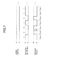
- Fig. 7 schematically illustrates the bit data (B1 to Bm) to be written to the word line (Wj), as well as the states of the memory cells (hereinafter, referred to as the resistance phases).
- the voltage V 1 is applied to B1, B4, B6 and B7 and the voltage V 0 is applied to B2, B3, and B5, since B1, B4, B6 and B7 correspond to a logic value of "1" and B2, B3, and B5 correspond to "0".
- the cells to which the voltage V 1 is applied make a phase transition from a high resistance phase (P H ) to a low resistance phase (P L ).
- the cells to which the voltage V 0 is applied retain a high resistance phase (P H ) since no phase transition takes place by the application of the voltage V 0 .
- the application voltage for the word line W j at time t j + ⁇ t is made 0V, and the voltage -V L is applied to the next word line W j+1 during the period ⁇ t.
- Data is also written to word lines W j+2 and beyond for each word in a similar manner.
- a read voltage V R is applied to all of the bit lines (B1-Bm). Further, a voltage V H that is equal to or more than V R is applied to the word lines. Alternatively, the word lines may be set at a high impedance. Also, as shown in Fig. 4, the read voltage V R is set to be a voltage so as not to cause a phase transition, that is, a voltage between the phase transition voltage +V w and 0V (0 ⁇ V R ⁇ +V W ).
- the written bit data can be read out by discriminating the resistance phase of each cell (that is, the high resistance phase or the low resistance phase thereof) from the current values.
- desired data can be read out by sequentially scanning the word lines at 0V.
- an erase voltage -V ER which is a voltage equal to or less than -V E , is applied to all of the word lines (W1-Wn) and all of the bit lines (B1 to Bm) at time t0. Then, at time t1, the voltage of all of the bit lines (B1 to Bm) is set to 0V.
- V E absolute value
- Fig. 10 is a cross-sectional view of a region which includes a memory cell portion of the memory device 10 according to a second embodiment of the present invention.
- the semiconductor layer 15 is formed as a p-type organic semiconductor for which the material used is copper phthalocyanine.
- a Schottky diode junction is formed at the interface with the semiconductor layer 15 by using a metal having a work function that is smaller than that of copper phthalocyanine, such as aluminum (Al), for example, for the upper electrode (word line Wj) 16.
- Al aluminum
- word line Wj upper electrode
- the Schottky diode exhibits a favorable switching characteristic and the cells C(j+1,i) thus operate as switching memory cells.
- Fig. 11 is a cross-sectional view of a region which includes a memory cell portion of the memory device 10 according to a third embodiment of the present invention.
- the configuration is produced by changing the position of the memory layer and the semiconductor layer of the first embodiment. More particularly, a bit line 12, a semiconductor layer 15, an organic memory layer 14, and a word line 16 are formed in this order on a substrate 11. Further, in this case, the semiconductor layer 15 is a p-n junction diode, for example, and is constituted such that the p-type semiconductor layer thereof makes contact with the lower electrode (bit line) 12.
- bit line lower electrode
- the word line and bit line are switched. More particularly, the lower electrode on the substrate 11 may constitute the word line, while the upper electrode may constitute the bit line.
- the diode polarity could also be the reverse of that of the above embodiment. In this case, the polarity of the application voltage may also be suitably selected in accordance with the polarity of the diode.
- the semiconductor layer 15 is not limited to an organic semiconductor.
- An inorganic semiconductor can also be used.
- a covalent bond semiconductor such as Si and a compound semiconductor such as GaAs can also be employed.
- the substrate 11 is not limited to alkali-free glass.
- plastics, organic materials and the like can also be employed. More particularly, because an organic material can be formed in a low temperature process, the material can be formed on a variety of substrates and the above configuration can therefore be implemented by means of a combination of a variety of materials.
- the first and second electrode lines need not be made of metal alone.
- the first and second electrode lines may be transparent electrodes made of an organic material or an ITO film (indium tin oxide film) or similar.
- the memory layer 14 can be formed by a variety of methods depending on the material used. Examples of other materials which can be used for the memory layer 14 include polymer materials such as hetero-aromatic polymers such as polythiophene and polypyrrole, polyphenylene polymers, polyaniline polymers, and polyacetylene polymers. Usage is not restricted to polymer materials, it also being possible to employ low molecular materials such as pentacene, tetracene, and anthracene. Further, the diode layer 15 can be formed using a material like that for the memory layer 14.
- the organic memory layer 14 and the organic semiconductor layer 15 are formed by vacuum deposition is described by way of example, but formation is not restricted to such a method.
- a variety of other deposition methods for organic materials can also be used.
- methods which can be employed include the Langmuir-Blodgett (LB) method, molecular self-assembly, molecular beam epitaxy (MBE), casting, spinning, melting, field polymerization, plasma polymerization, and the like.
- n-type (donor) dopant of the semiconductor layer 15 an alkali metal such as sodium (Na), potassium (K), and alkyl ammonium and the like can be used.
- an alkali metal such as sodium (Na), potassium (K), and alkyl ammonium and the like
- the semiconductor layer 15 is constituted by a p-type organic semiconductor, a variety of substances can be employed as the p-type (acceptor) dopant, such as halogens, Lewis acid, protic acid, transition metal chlorides, and the like.
- polymer dopants can be used as the dopant in addition to the above-mentioned dopants.
- a polymer electrolyte such as polystyrene sulfonate and polyvinyl sulfonate can be used.
- ion implantation which involves accelerating ionized dopant by means of an electric field to inject the dopant into organic material
- induced doping which employs light and radiation to perform doping
Landscapes
- Engineering & Computer Science (AREA)
- Chemical & Material Sciences (AREA)
- Nanotechnology (AREA)
- Physics & Mathematics (AREA)
- Mathematical Physics (AREA)
- Theoretical Computer Science (AREA)
- Crystallography & Structural Chemistry (AREA)
- Semiconductor Memories (AREA)
- Read Only Memory (AREA)
Abstract
Description
- The present invention relates to an organic switching memory device that permits writing and rewriting and in which organic material is employed, and to a memory apparatus or the like having the memory device.
- In recent years, research and development has vigorously pursued developing functional devices or electronic elements employing organic material. Examples of conventional memory devices employing organic materials include, for example, a mask ROM (Read Only Memory) that utilizes an organic diode as disclosed by Japanese Patent Kohyo No. 2001-516964. Because the memory device does not permit electrical writing, the use of the memory device is limited to a mask ROM and the memory element cannot therefore be applied to a memory device that is capable of performing electrical writing or rewriting operations.
- Furthermore, examples of other memory devices include the memory device disclosed by Japanese Patent Kokai No. 08-116109. The memory device utilizes a material which changes in resistance in accordance with the application of a voltage and retains the resistance value even upon removal of the application voltage. Although such a memory device must be combined with a switching element for increasing the capacity of a memory device, a straightforward method has not been proposed in which the characteristics of the organic material are utilized.
- The prior art has therefore been confronted by a problem such that it is difficult to implement a large-capacity organic memory device and a memory apparatus that permits electrical writing or rewriting in a high-performance organic memory device or memory apparatus. The problem mentioned above is cited as one example of the problems which the present invention is intended to resolve.
- According to the present invention, there is provided an organic switching memory device, which comprises a plurality of first electrode lines; an organic memory layer formed on the plurality of first electrode lines, the organic memory layer exhibiting a voltage-current hysteresis characteristic; a semiconductor diode layer stacked on the organic memory layer; and a plurality of second electrode lines formed on the semiconductor diode layer, the plurality of second electrode lines being disposed in a direction so as to intersect the plurality of first electrode lines.
- Further, according to the present invention, there is provided a memory apparatus which comprises a organic switching memory device having a plurality of first electrode lines, an organic memory layer formed on the plurality of first electrode lines, the organic memory layer exhibiting a voltage-current hysteresis characteristic; a semiconductor diode layer stacked on the organic memory layer; and a plurality of second electrode lines formed on the semiconductor diode layer, the plurality of second electrode lines being disposed in a direction so as to intersect the plurality of first electrode lines, a receiver section for receiving an address designation signal, data and a write command signal, the address designation signal designating addresses which correspond to intersecting positions of the plurality of first electrode lines and the plurality of second electrode lines, and a control section which writes the data to the organic switching memory device on the basis of the address designation signal, in response to the write command signal.
-
- Fig. 1 is a plan view of part of a memory device according to the first embodiment of the present invention;
- Fig. 2 is a cross-sectional view of a region which comprises a memory cell portion of the memory device shown in Fig. 1;
- Fig. 3 corresponds to Fig. 1 and shows an electrical equivalent circuit for part of the memory device;
- Fig. 4 shows an example of the current-voltage characteristic (I-V characteristic) of the organic memory material employed for the memory layer;
- Fig. 5 shows the configuration of a memory device that uses the memory device;
- Fig. 6 is a time chart that serves to illustrate the procedure for a case where data is written to the memory device a word at a time;
- Fig. 7 schematically shows bit data (B1-Bm) written to a word line Wj when a voltage -VL is applied to the word line Wj at a time tj, as well as the states of the memory cells;
- Fig. 8 is a time chart that serves to illustrate the procedure in a case where data is read out from the memory device a word at a time;
- Fig. 9 is a time chart that serves to illustrate the procedure in a case where the contents of all of the memory cells are erased (reset);
- Fig. 10 is a cross-sectional view of a region which comprises a memory cell portion of the memory device according to a second embodiment of the present invention; and
- Fig. 11 is a cross-sectional view of a region which comprises a memory cell portion of the memory device according to a third embodiment of the present invention.
-
- Embodiments of the present invention will now be described in detail with reference to the drawings. In the figures which are referenced in the following description, the same reference numerals are assigned to the constituent elements which are substantially equivalent.
- Fig. 1 is a plan view of part of a
memory device 10 according to a first embodiment of the present invention, and Fig. 2 is a cross-sectional view of a region that comprises a memory cell portion of thememory device 10 shown in Fig. 1. As shown in Fig. 1, thememory device 10 is constituted by stacking, on asubstrate 11, a lower electrode (hereinafter, also referred to as bit lines Bi) 12, amemory layer 14, asemiconductor layer 15, and an upper electrode (hereinafter, also referred to as word lines Wj) 16, in this order. - In more detail, the
substrate 11 is constituted by alkali-free glass, for example. A plurality of first electrode lines made of a gold (Au) metal layer or other metal layer, that is, bit lines Bi (i=1, 2, . . .m). are arranged in the form of mutually parallel stripes or strips on thesubstrate 11. Thememory layer 14 is formed by an organic memory material such as zinc phthalocyanine (ZnPc) or zinc phthalocyanine porphyrin, for example. Thesemiconductor layer 15 is a p-n junction organic semiconductor diode in which copper phthalocyanine is used as the p-type material and a perylene derivative is used as the n-type material, for example. The p-type organic semiconductor layer is connected to thememory layer 14 and the n-type organic semiconductor layer is connected to theupper electrode 16 described hereinafter. - A plurality of second electrode lines provided by a metal such as aluminum (Al), that is, stripe-shaped word lines Wj (j=1, 2, . . .n), are arranged on the
semiconductor layer 15 so as to be mutually parallel and lie in a direction that sterically intersects bit lines Bi, in a direction orthogonal to bit lines Bi, for example. An ohmic contact is formed between the upper electrode (word lines Wj) 16 and the semiconductor layer 15 (n-type organic semiconductor layer). - The lower electrode (bit lines Bi) 12, the
memory layer 14, thesemiconductor layer 15 and the upper electrode (word lines Wj) 16 are formed by means of vacuum vapor deposition. - According to the above-mentioned configuration, memory cells C(j,i) are formed in the regions of intersections between the word lines Wj and the bit lines Bi. More particularly, each of the memory cells C(j,i) has a structure in which the word line (Wj) 16, the semiconductor layer (diode junction) 15, the
memory layer 14 and the bit line (Bi) 12 are connected in series. Further, the memory cells C(j,i) are arranged in the form of a matrix. As will be described later, the memory cells C(j,i) serve as switching memory composite elements. - Fig. 3 corresponds to Fig. 1 and shows an electrical equivalent circuit corresponding to a part of the
memory device 10. In the equivalent circuit, the diodes Di corresponds to the diode junction of thesemiconductor layer 15 and the resistors R corresponds to the memory layer 14 (Fig. 2). Each of the memory cells C(j,i) can be represented as a serial connection of the diode Di and the resistor R. - Fig. 4 shows an example of the current-voltage characteristic (I-V characteristic) of the organic memory material (zinc phthalocyanine: ZnPc) employed for the
memory layer 14 . Such an organic memory material exhibits a hysteresis loop characteristic. More particularly, when the memory material is in a high-resistance phase state (reset state), the current value increases in accordance with the resistance value of the high-resistance phase region as the voltage applied to the memory material is increased. As the application voltage approaches Vw, the current value starts to increase rapidly, and the memory material makes a phase transition to a low resistance phase when the application voltage reaches +Vw (Vw >0). Further, the current value decreases in accordance with the resistance value in the low resistance phase region as the application voltage is decreased from the transition voltage Vw. When the application voltage is reduced further and the application voltage reaches -VE (VE>0), the current value increases abruptly and the memory material makes the phase transition to a high resistance phase. It should be noted that a case is illustrated, for brevity of the description, in which the current value varies substantially linearly in the high resistance phase region and the low resistance phase region. However, a memory material may also be used that has an I-V hysteresis characteristic such that current variations have the form of a curve. - As described above, the memory material makes the phase transition to the low resistance phase by an application of a voltage that is equal to or greater than +Vw(Vw>0), and makes the phase transition to the high resistance phase by an application of a voltage that is equal to or less than -VE(VE>0). Therefore, writing of binary data can be performed by varying the voltage which is applied to the memory cells through the use of the I-V characteristic of the memory material. Furthermore, as shown in Fig. 4, the data thus written can be read out by applying a voltage VR that lies between -VE and +Vw to the memory device or cell to detect the difference in the electric current values (that is, for example, I0 and I1).
- Fig. 5 shows the configuration of a
memory apparatus 20 that uses amemory device 10. Thememory apparatus 20 comprises amemory device 10, which includes the above-mentioned matrix memory array, acontroller 21, anaddress selection circuit 23, and a write/read control circuit (hereinafter, simply referred to as a 'write/read circuit') 24. Address designation signals are supplied from thecontroller 21 to theaddress selection circuit 23, and a write control signal or a read control signal is supplied from thecontroller 21 to the write/read circuit 24. Theaddress selection circuit 23 may include an address register (not shown). The write/read circuit 24 may include a write register/read register (not shown). Thecontroller 21 performs writing to thememory device 10 on the basis of external data and control signals or on the basis of control signals and data which are generated internally, and outputs data read out from thememory device 10. Further, thecontroller 21 performs an erase operation and a total reset operation of written data to the memory cells. - In addition, the
memory device 20 may include circuits for providing an increased speed or increased functionality such as an error correction circuit, a refresh circuit, and a buffer circuit. Further, thecontroller 21 need not be provided as a separate circuit as shown in Fig. 5. Also, a configuration is also possible in which the apparatus does not include thecontroller 21. In such an apparatus, theaddress selection circuit 23 and the write/read circuit 24 are configured to operate in accordance with commands supplied via a data bus or the like from an external processor such as a microprocessor (CPU), for example so as to perform the write/read and erase operations of thememory device 10. - A detailed description is provided below with reference to the drawings with regards to the principles of the write, read and erase operations of the
memory device 10. Further, for the purpose of simplifying the description, the assumption is made that all of the memory cells C(j,i) are reset to "0" (logic value) when a write operation is performed. Here, the high resistance phase and the low resistance phase correspond to "0" and "1" (logic values), respectively. - A case in which data is written to the memory device 10 a word at a time (i.e., word-by-word) will be described by way of example. More particularly, the voltage of a word line for performing a write operation is set to -VL (VL>0) , and a voltage V1 (V1>0) is applied to cells to be written with "1", and a voltage V0 (V0>0) is applied to cells to be written with "0". In this instance, the voltages V1 and V0 are set so that V1-VL > Vw, and V0 - V1 < Vw. Further, a voltage (0V in the present embodiment) is applied to the word lines which are not to undergo writing, the voltage being sufficiently high in order to avoid a phase transition as a result of the application of the voltage V1. Alternatively, the word lines which are not to undergo writing may be held at a high impedance.
- More specifically, as shown in Fig. 6, the voltage -VL is applied to the j-th word line (Wj) which is to undergo writing at time tj. The application of the voltage to the word line (Wj) takes place during the period Δt. In this instance, the voltage V1 or V0 is applied in correspondence with each bit of the bit data to be written to the bit lines Bi (i= 1,2,... m). Fig. 7 schematically illustrates the bit data (B1 to Bm) to be written to the word line (Wj), as well as the states of the memory cells (hereinafter, referred to as the resistance phases). For example, when the bit data which is to be written to the word line (Wj) is "1001011..." , the voltage V1 is applied to B1, B4, B6 and B7 and the voltage V0 is applied to B2, B3, and B5, since B1, B4, B6 and B7 correspond to a logic value of "1" and B2, B3, and B5 correspond to "0". As described above, the cells to which the voltage V1 is applied make a phase transition from a high resistance phase (PH) to a low resistance phase (PL). Further, the cells to which the voltage V0 is applied retain a high resistance phase (PH) since no phase transition takes place by the application of the voltage V0. Accordingly, the memory cells C(j, i) on the word line Wj (where i= 1,2,3, ...), have resistance phases "LHHLHLL... " in correspondence with the bit data (here, PH is denoted by "H", and PL is denoted by "L").
- Then, as shown in Fig. 6, the application voltage for the word line Wj at time tj+Δt is made 0V, and the voltage -VL is applied to the next word line Wj+1 during the period Δt. The voltage V1 or V0 is applied to the bit lines Bi (i= 1,2,... m) in accordance with each bit of the bit data to be written to the cells on the word line Wj+1. As a result, in a similar manner as described above, the cells C(j+1,i) (where i= 1,2,3, . . .m) on the word line Wj+1 have resistance phases in accordance with the bit data. Data is also written to word lines Wj+2 and beyond for each word in a similar manner.
- A description will be provided next for the procedure for reading out data from the
memory device 10 for each word. More particularly, as shown in Fig. 8, a read voltage VR is applied to all of the bit lines (B1-Bm). Further, a voltage VH that is equal to or more than VR is applied to the word lines. Alternatively, the word lines may be set at a high impedance. Also, as shown in Fig. 4, the read voltage VR is set to be a voltage so as not to cause a phase transition, that is, a voltage between the phase transition voltage +Vw and 0V (0<VR<+VW). In this condition, the voltage of the word line (Wj) to be read out is changed to be 0V, whereby the respective values of the current flowing in the memory cells C(j+1,i) (where i=1,2,3...m) are detected. The written bit data can be read out by discriminating the resistance phase of each cell (that is, the high resistance phase or the low resistance phase thereof) from the current values. Similarly to a case in which data is written, desired data can be read out by sequentially scanning the word lines at 0V. - A description will be provided next for the procedure whereby data written to the
memory device 10 is erased. Further, a case in which the contents of all of the memory cells are erased (or reset) will be described by way of example. First of all, as shown in Fig. 9, an erase voltage -VER, which is a voltage equal to or less than -VE, is applied to all of the word lines (W1-Wn) and all of the bit lines (B1 to Bm) at time t0. Then, at time t1, the voltage of all of the bit lines (B1 to Bm) is set to 0V. Because a voltage that is equal to or greater than VE (absolute value) is applied across the memory cells at the instant the voltage of all the bit lines is set to 0V, the memory cells are reset to a high resistance phase irrespective of the state (resistance phase) prior to this erasure. Further, a case in which the contents of all of the memory cells are erased (reset) is described above, however, erasure could also be performed for each word or each cell. - Therefore, as described above, according to the present invention, it is possible to provide a switching memory device that is simple and inexpensive and permits electrical writing and readout, as well as a memory apparatus which employs the memory device.
- Fig. 10 is a cross-sectional view of a region which includes a memory cell portion of the
memory device 10 according to a second embodiment of the present invention. Thesemiconductor layer 15 is formed as a p-type organic semiconductor for which the material used is copper phthalocyanine. A Schottky diode junction is formed at the interface with thesemiconductor layer 15 by using a metal having a work function that is smaller than that of copper phthalocyanine, such as aluminum (Al), for example, for the upper electrode (word line Wj) 16. The configuration of the other portions of thememory device 10 is similar as that of the first embodiment. - Similarly to the case of the first embodiment described above, the Schottky diode exhibits a favorable switching characteristic and the cells C(j+1,i) thus operate as switching memory cells.
- Fig. 11 is a cross-sectional view of a region which includes a memory cell portion of the
memory device 10 according to a third embodiment of the present invention. In this embodiment, the configuration is produced by changing the position of the memory layer and the semiconductor layer of the first embodiment. More particularly, abit line 12, asemiconductor layer 15, anorganic memory layer 14, and aword line 16 are formed in this order on asubstrate 11. Further, in this case, thesemiconductor layer 15 is a p-n junction diode, for example, and is constituted such that the p-type semiconductor layer thereof makes contact with the lower electrode (bit line) 12. The configuration is in other respects similar to the first embodiment. - Further, a variety of additional modifications are possible for the above-described first to third embodiments. For example, a configuration is possible in which the word line and bit line are switched. More particularly, the lower electrode on the
substrate 11 may constitute the word line, while the upper electrode may constitute the bit line. In addition, the diode polarity could also be the reverse of that of the above embodiment. In this case, the polarity of the application voltage may also be suitably selected in accordance with the polarity of the diode. - Further, the
semiconductor layer 15 is not limited to an organic semiconductor. An inorganic semiconductor can also be used. For example, a covalent bond semiconductor such as Si and a compound semiconductor such as GaAs can also be employed. - Also, for example, the
substrate 11 is not limited to alkali-free glass. For example, plastics, organic materials and the like can also be employed. More particularly, because an organic material can be formed in a low temperature process, the material can be formed on a variety of substrates and the above configuration can therefore be implemented by means of a combination of a variety of materials. - The first and second electrode lines need not be made of metal alone. The first and second electrode lines may be transparent electrodes made of an organic material or an ITO film (indium tin oxide film) or similar.
- In addition, a variety of materials other than the above-mentioned phthalocyanine materials can be employed for the
memory layer 14. Thememory layer 14 can be formed by a variety of methods depending on the material used. Examples of other materials which can be used for thememory layer 14 include polymer materials such as hetero-aromatic polymers such as polythiophene and polypyrrole, polyphenylene polymers, polyaniline polymers, and polyacetylene polymers. Usage is not restricted to polymer materials, it also being possible to employ low molecular materials such as pentacene, tetracene, and anthracene. Further, thediode layer 15 can be formed using a material like that for thememory layer 14. - In addition, a case in which the
organic memory layer 14 and theorganic semiconductor layer 15 are formed by vacuum deposition is described by way of example, but formation is not restricted to such a method. A variety of other deposition methods for organic materials can also be used. For example, methods which can be employed include the Langmuir-Blodgett (LB) method, molecular self-assembly, molecular beam epitaxy (MBE), casting, spinning, melting, field polymerization, plasma polymerization, and the like. - Further, as the n-type (donor) dopant of the
semiconductor layer 15, an alkali metal such as sodium (Na), potassium (K), and alkyl ammonium and the like can be used. Further, in cases where thesemiconductor layer 15 is constituted by a p-type organic semiconductor, a variety of substances can be employed as the p-type (acceptor) dopant, such as halogens, Lewis acid, protic acid, transition metal chlorides, and the like. - Furthermore, so-called polymer dopants can be used as the dopant in addition to the above-mentioned dopants. For example, a polymer electrolyte such as polystyrene sulfonate and polyvinyl sulfonate can be used.
- As methods for doping the above-mentioned organic materials, a variety of methods can be employed such as gas phase and liquid phase doping and electrochemical doping and the like. Alternatively, ion implantation, which involves accelerating ionized dopant by means of an electric field to inject the dopant into organic material, and induced doping, which employs light and radiation to perform doping, can be used.
- The invention has been described with reference to the preferred embodiments thereof. It should be understood by those skilled in the art that a variety of alterations and modifications may be made from the embodiments described above. It is therefore contemplated that the appended claims encompass all such alterations and modifications.
Claims (5)
- An organic switching memory device, comprising:a plurality of first electrode lines;an organic memory layer formed on said plurality of first electrode lines, said organic memory layer having a voltage-current hysteresis characteristic;a semiconductor diode layer stacked on said organic memory layer; anda plurality of second electrode lines formed on said semiconductor diode layer, said plurality of second electrode lines being disposed in a direction so as to intersect said plurality of first electrode lines.
- The organic switching memory device according to claim 1, wherein said semiconductor diode layer is a pn-junction diode layer.
- The organic switching memory device according to claim 1, wherein said semiconductor diode layer is a Schottky diode layer.
- A memory apparatus, comprising:a organic switching memory device including:a plurality of first electrode lines;an organic memory layer formed on said plurality of first electrode lines, said organic memory layer having a voltage-current hysteresis characteristic;a semiconductor diode layer stacked on said organic memory layer; anda plurality of second electrode lines formed on said semiconductor diode layer, said plurality of second electrode lines being disposed in a direction so as to intersect said plurality of first electrode lines,a receiver section for receiving an address designation signal, data and a write command signal, said address designation signal designating addresses which correspond to intersecting positions of said plurality of first electrode lines and said plurality of second electrode lines, anda control section which writes the data to said organic switching memory device on the basis of the address designation signal, in response to the write command signal.
- The memory apparatus according to claim 4, wherein:said receiver section receives a read command signal, andsaid control section reads out data from said organic switching memory device on the basis of said address designation signal, in response to said read command signal.
Applications Claiming Priority (2)
| Application Number | Priority Date | Filing Date | Title |
|---|---|---|---|
| JP2002204102 | 2002-07-12 | ||
| JP2002204102A JP2004047791A (en) | 2002-07-12 | 2002-07-12 | Organic thin film switching memory element and memory device |
Publications (2)
| Publication Number | Publication Date |
|---|---|
| EP1381054A1 true EP1381054A1 (en) | 2004-01-14 |
| EP1381054B1 EP1381054B1 (en) | 2005-09-28 |
Family
ID=29728530
Family Applications (1)
| Application Number | Title | Priority Date | Filing Date |
|---|---|---|---|
| EP03014548A Expired - Lifetime EP1381054B1 (en) | 2002-07-12 | 2003-07-07 | Organic memory device |
Country Status (5)
| Country | Link |
|---|---|
| US (1) | US6947321B2 (en) |
| EP (1) | EP1381054B1 (en) |
| JP (1) | JP2004047791A (en) |
| CN (1) | CN1481034A (en) |
| DE (1) | DE60301703T2 (en) |
Cited By (15)
| Publication number | Priority date | Publication date | Assignee | Title |
|---|---|---|---|---|
| FR2864677A1 (en) * | 2004-05-12 | 2005-07-01 | Thomson Licensing Sa | ORGANIC ELECTROLUMINESCENT PANEL WITH BI-STABLE ELEMENTS FORMED BY A SINGLE ORGANIC LAYER |
| WO2005124787A3 (en) * | 2004-06-16 | 2006-03-16 | Koninkl Philips Electronics Nv | Electrical device having a programmable resistor connected in series to a punch-through diode and method of manufacturing therefor |
| WO2006095278A1 (en) * | 2005-03-07 | 2006-09-14 | Nxp B.V. | Driving of a memory matrix of resistance hysteresis elements |
| WO2007105575A1 (en) * | 2006-03-10 | 2007-09-20 | Semiconductor Energy Laboratory Co., Ltd. | Memory element and semiconductor device |
| US7580275B2 (en) | 2005-03-09 | 2009-08-25 | Nxp B.V. | Control of a memory matrix with resistance hysteresis elements |
| US7611965B2 (en) | 2005-08-31 | 2009-11-03 | Semiconductor Energy Laboratory Co., Ltd. | Semiconductor device and manufacturing method thereof |
| US7700984B2 (en) | 2005-05-20 | 2010-04-20 | Semiconductor Energy Laboratory Co., Ltd | Semiconductor device including memory cell |
| US7745252B2 (en) | 2005-08-31 | 2010-06-29 | Semiconductor Energy Laboratory Co., Ltd. | Semiconductor device and manufacturing method thereof |
| US7791066B2 (en) | 2005-05-20 | 2010-09-07 | Semiconductor Energy Laboratory Co., Ltd. | Semiconductor device and manufacturing method thereof and method for writing memory element |
| US7956352B2 (en) | 2005-03-25 | 2011-06-07 | Semiconductor Energy Laboratory Co., Ltd. | Memory element comprising an organic compound and an insulator |
| US7960719B2 (en) | 2004-12-03 | 2011-06-14 | Semiconductor Energy Laboratotry Co., Ltd. | Semiconductor device |
| US8089799B2 (en) | 2004-10-18 | 2012-01-03 | Semiconductor Energy Laboratory Co., Ltd. | Semiconductor device and driving method of the same |
| US8173519B2 (en) | 2006-03-03 | 2012-05-08 | Semiconductor Energy Laboratory Co., Ltd. | Method for manufacturing semiconductor device |
| US8222116B2 (en) | 2006-03-03 | 2012-07-17 | Semiconductor Energy Laboratory Co., Ltd. | Method for manufacturing semiconductor device |
| US8288197B2 (en) | 2005-04-27 | 2012-10-16 | Semiconductor Energy Laboratory Co., Ltd. | Method for manufacturing a semiconductor device including a memory device comprising an insulator mixture region in a conductive layer |
Families Citing this family (36)
| Publication number | Priority date | Publication date | Assignee | Title |
|---|---|---|---|---|
| CA2500938A1 (en) * | 2004-03-24 | 2005-09-24 | Rohm And Haas Company | Memory devices based on electric field programmable films |
| US7795617B2 (en) * | 2004-10-29 | 2010-09-14 | Semiconductor Energy Laboratory Co., Ltd. | Semiconductor device, IC card, IC tag, RFID, transponder, paper money, valuable securities, passport, electronic device, bag, and clothes |
| US9734901B2 (en) * | 2004-10-29 | 2017-08-15 | Semiconductor Energy Laboratory Co., Ltd. | Display device with semiconductor memory cell |
| US7688624B2 (en) | 2004-11-26 | 2010-03-30 | Semiconductor Energy Laboratory Co., Ltd. | Semiconductor device |
| JP4912671B2 (en) * | 2004-11-26 | 2012-04-11 | 株式会社半導体エネルギー研究所 | Semiconductor device |
| US7919772B2 (en) | 2004-12-14 | 2011-04-05 | Semiconductor Energy Laboratory Co., Ltd. | Semiconductor device and manufacturing method thereof |
| US7443711B1 (en) | 2004-12-16 | 2008-10-28 | Hewlett-Packard Development Company, L.P. | Non-volatile programmable impedance nanoscale devices |
| US7379317B2 (en) * | 2004-12-23 | 2008-05-27 | Spansion Llc | Method of programming, reading and erasing memory-diode in a memory-diode array |
| EP1846952A4 (en) * | 2005-02-10 | 2012-11-07 | Semiconductor Energy Lab | SEMICONDUCTOR DEVICE AND METHOD FOR MANUFACTURING THE SAME |
| CN100546034C (en) | 2005-02-10 | 2009-09-30 | 株式会社半导体能源研究所 | Semiconductor device and manufacturing method thereof |
| JP4974555B2 (en) * | 2005-03-25 | 2012-07-11 | 株式会社半導体エネルギー研究所 | Memory element |
| TWI467702B (en) | 2005-03-28 | 2015-01-01 | 半導體能源研究所股份有限公司 | Memory device and method of manufacturing same |
| CN100456514C (en) * | 2005-04-18 | 2009-01-28 | 中国科学院长春应用化学研究所 | Single-layer organic memory and its manufacturing method |
| US7369424B2 (en) * | 2005-11-09 | 2008-05-06 | Industrial Technology Research Institute | Programmable memory cell and operation method |
| TWI267850B (en) * | 2005-12-30 | 2006-12-01 | Ind Tech Res Inst | Bit cell of organic memory |
| JP5201853B2 (en) * | 2006-03-10 | 2013-06-05 | 株式会社半導体エネルギー研究所 | Semiconductor device |
| US7923719B2 (en) | 2006-04-28 | 2011-04-12 | Semiconductor Energy Laboratory Co., Ltd. | Semiconductor memory device wherein wiring contact is made through an opening in an organic compound layer |
| EP1850378A3 (en) | 2006-04-28 | 2013-08-07 | Semiconductor Energy Laboratory Co., Ltd. | Memory device and semicondutor device |
| JP5171129B2 (en) * | 2006-06-28 | 2013-03-27 | 株式会社半導体エネルギー研究所 | Semiconductor device |
| US7719001B2 (en) * | 2006-06-28 | 2010-05-18 | Semiconductor Energy Laboratory Co., Ltd | Semiconductor device with metal oxides and an organic compound |
| EP1883109B1 (en) * | 2006-07-28 | 2013-05-15 | Semiconductor Energy Laboratory Co., Ltd. | Memory element and method of manufacturing thereof |
| US7988057B2 (en) | 2006-11-28 | 2011-08-02 | Semiconductor Energy Laboratory Co., Ltd. | Memory device and semiconductor device |
| US7875881B2 (en) * | 2007-04-03 | 2011-01-25 | Semiconductor Energy Laboratory Co., Ltd. | Memory device and semiconductor device |
| DE102007028236A1 (en) * | 2007-06-20 | 2009-01-02 | Siemens Ag | Semiconducting material and organic rectifier diode |
| WO2009020210A1 (en) * | 2007-08-08 | 2009-02-12 | National Institute For Materials Science | Switching element and application of the same |
| US20110199356A1 (en) * | 2007-12-06 | 2011-08-18 | Pioneer Corporation | Pixel circuit and display panel |
| US8019642B2 (en) * | 2008-05-06 | 2011-09-13 | Richrelevance, Inc. | System and process for receiving boosting recommendations for use in providing personalized advertisements to retail customers |
| JP5717490B2 (en) | 2011-03-24 | 2015-05-13 | 株式会社東芝 | Organic molecular memory |
| DE102015000120A1 (en) * | 2015-01-07 | 2016-07-07 | Merck Patent Gmbh | Electronic component |
| US10833264B2 (en) * | 2016-03-23 | 2020-11-10 | Forschungszentrum Juelich Gmbh | Method for producing a memory cell having a porous dielectric and use of the memory cell |
| WO2018020333A1 (en) | 2016-07-29 | 2018-02-01 | Semiconductor Energy Laboratory Co., Ltd. | Separation method, display device, display module, and electronic device |
| TWI753868B (en) | 2016-08-05 | 2022-02-01 | 日商半導體能源研究所股份有限公司 | Peeling method, display device, display module and electronic device |
| TWI730017B (en) | 2016-08-09 | 2021-06-11 | 日商半導體能源研究所股份有限公司 | Manufacturing method of display device, display device, display module and electronic device |
| US10923350B2 (en) | 2016-08-31 | 2021-02-16 | Semiconductor Energy Laboratory Co., Ltd. | Manufacturing method of semiconductor device |
| CN109564851A (en) | 2016-08-31 | 2019-04-02 | 株式会社半导体能源研究所 | Manufacturing method of semiconductor device |
| US10369664B2 (en) | 2016-09-23 | 2019-08-06 | Semiconductor Energy Laboratory Co., Ltd. | Manufacturing method of semiconductor device |
Citations (2)
| Publication number | Priority date | Publication date | Assignee | Title |
|---|---|---|---|---|
| JPH08116109A (en) * | 1994-10-14 | 1996-05-07 | Matsushita Giken Kk | Organic thin film switching memory composite element manufacturing method and organic thin film switching memory composite element |
| US6055180A (en) * | 1997-06-17 | 2000-04-25 | Thin Film Electronics Asa | Electrically addressable passive device, method for electrical addressing of the same and uses of the device and the method |
Family Cites Families (3)
| Publication number | Priority date | Publication date | Assignee | Title |
|---|---|---|---|---|
| NO973993L (en) | 1997-09-01 | 1999-03-02 | Opticom As | Reading memory and reading memory devices |
| US6646912B2 (en) * | 2001-06-05 | 2003-11-11 | Hewlett-Packard Development Company, Lp. | Non-volatile memory |
| US6683322B2 (en) * | 2002-03-01 | 2004-01-27 | Hewlett-Packard Development Company, L.P. | Flexible hybrid memory element |
-
2002
- 2002-07-12 JP JP2002204102A patent/JP2004047791A/en active Pending
-
2003
- 2003-07-07 EP EP03014548A patent/EP1381054B1/en not_active Expired - Lifetime
- 2003-07-07 DE DE60301703T patent/DE60301703T2/en not_active Expired - Fee Related
- 2003-07-10 US US10/616,501 patent/US6947321B2/en not_active Expired - Fee Related
- 2003-07-11 CN CNA031526845A patent/CN1481034A/en active Pending
Patent Citations (2)
| Publication number | Priority date | Publication date | Assignee | Title |
|---|---|---|---|---|
| JPH08116109A (en) * | 1994-10-14 | 1996-05-07 | Matsushita Giken Kk | Organic thin film switching memory composite element manufacturing method and organic thin film switching memory composite element |
| US6055180A (en) * | 1997-06-17 | 2000-04-25 | Thin Film Electronics Asa | Electrically addressable passive device, method for electrical addressing of the same and uses of the device and the method |
Non-Patent Citations (1)
| Title |
|---|
| PATENT ABSTRACTS OF JAPAN vol. 1996, no. 09 30 September 1996 (1996-09-30) * |
Cited By (28)
| Publication number | Priority date | Publication date | Assignee | Title |
|---|---|---|---|---|
| FR2864677A1 (en) * | 2004-05-12 | 2005-07-01 | Thomson Licensing Sa | ORGANIC ELECTROLUMINESCENT PANEL WITH BI-STABLE ELEMENTS FORMED BY A SINGLE ORGANIC LAYER |
| WO2005124787A3 (en) * | 2004-06-16 | 2006-03-16 | Koninkl Philips Electronics Nv | Electrical device having a programmable resistor connected in series to a punch-through diode and method of manufacturing therefor |
| US8089799B2 (en) | 2004-10-18 | 2012-01-03 | Semiconductor Energy Laboratory Co., Ltd. | Semiconductor device and driving method of the same |
| US8223531B2 (en) | 2004-10-18 | 2012-07-17 | Semiconductor Energy Laboratory Co., Ltd. | Semiconductor device and driving method of the same |
| US8507902B2 (en) | 2004-12-03 | 2013-08-13 | Semiconductor Energy Laboratory Co., Ltd. | Semiconductor device |
| US7960719B2 (en) | 2004-12-03 | 2011-06-14 | Semiconductor Energy Laboratotry Co., Ltd. | Semiconductor device |
| WO2006095278A1 (en) * | 2005-03-07 | 2006-09-14 | Nxp B.V. | Driving of a memory matrix of resistance hysteresis elements |
| US7643327B2 (en) | 2005-03-07 | 2010-01-05 | Nxp B.V. | Driving a memory matrix of resistance hysteresis elements |
| US7580275B2 (en) | 2005-03-09 | 2009-08-25 | Nxp B.V. | Control of a memory matrix with resistance hysteresis elements |
| US8399881B2 (en) | 2005-03-25 | 2013-03-19 | Semiconductor Energy Laboratory Co., Ltd. | Memory element, memory device, and semiconductor device |
| US7956352B2 (en) | 2005-03-25 | 2011-06-07 | Semiconductor Energy Laboratory Co., Ltd. | Memory element comprising an organic compound and an insulator |
| US8288197B2 (en) | 2005-04-27 | 2012-10-16 | Semiconductor Energy Laboratory Co., Ltd. | Method for manufacturing a semiconductor device including a memory device comprising an insulator mixture region in a conductive layer |
| US8174006B2 (en) | 2005-05-20 | 2012-05-08 | Semiconductor Energy Laboratory Co., Ltd. | Semiconductor device and manufacturing method thereof and method for writing memory element |
| US7700984B2 (en) | 2005-05-20 | 2010-04-20 | Semiconductor Energy Laboratory Co., Ltd | Semiconductor device including memory cell |
| US7791066B2 (en) | 2005-05-20 | 2010-09-07 | Semiconductor Energy Laboratory Co., Ltd. | Semiconductor device and manufacturing method thereof and method for writing memory element |
| US7611965B2 (en) | 2005-08-31 | 2009-11-03 | Semiconductor Energy Laboratory Co., Ltd. | Semiconductor device and manufacturing method thereof |
| US7745252B2 (en) | 2005-08-31 | 2010-06-29 | Semiconductor Energy Laboratory Co., Ltd. | Semiconductor device and manufacturing method thereof |
| US9082679B2 (en) | 2006-03-03 | 2015-07-14 | Semiconductor Energy Laboratory Co., Ltd. | Method for manufacturing semiconductor device |
| US8222116B2 (en) | 2006-03-03 | 2012-07-17 | Semiconductor Energy Laboratory Co., Ltd. | Method for manufacturing semiconductor device |
| US8823023B2 (en) | 2006-03-03 | 2014-09-02 | Semiconductor Energy Laboratory Co., Ltd. | Method for manufacturing semiconductor device |
| US8173519B2 (en) | 2006-03-03 | 2012-05-08 | Semiconductor Energy Laboratory Co., Ltd. | Method for manufacturing semiconductor device |
| US9419142B2 (en) | 2006-03-03 | 2016-08-16 | Semiconductor Energy Laboratory Co., Ltd. | Method for manufacturing semiconductor device |
| US9436036B2 (en) | 2006-03-03 | 2016-09-06 | Semiconductor Energy Laboratory Co., Ltd. | Method for manufacturing semiconductor device |
| US9793150B2 (en) | 2006-03-03 | 2017-10-17 | Semiconductor Energy Laboratory Co., Ltd. | Method for manufacturing semiconductor device |
| US10229940B2 (en) | 2006-03-03 | 2019-03-12 | Semiconductor Energy Laboratory Co., Ltd. | Method for manufacturing semiconductor device |
| US10818703B2 (en) | 2006-03-03 | 2020-10-27 | Semiconductor Energy Laboratory Co., Ltd. | Method for manufacturing semiconductor device |
| US8421061B2 (en) | 2006-03-10 | 2013-04-16 | Semiconductor Energy Laboratory Co., Ltd. | Memory element and semiconductor device including the memory element |
| WO2007105575A1 (en) * | 2006-03-10 | 2007-09-20 | Semiconductor Energy Laboratory Co., Ltd. | Memory element and semiconductor device |
Also Published As
| Publication number | Publication date |
|---|---|
| JP2004047791A (en) | 2004-02-12 |
| US20040057323A1 (en) | 2004-03-25 |
| US6947321B2 (en) | 2005-09-20 |
| EP1381054B1 (en) | 2005-09-28 |
| DE60301703T2 (en) | 2006-07-06 |
| DE60301703D1 (en) | 2005-11-03 |
| CN1481034A (en) | 2004-03-10 |
Similar Documents
| Publication | Publication Date | Title |
|---|---|---|
| EP1381054B1 (en) | Organic memory device | |
| US6781868B2 (en) | Molecular memory device | |
| US7254053B2 (en) | Active programming and operation of a memory device | |
| Möller et al. | Electrochromic conductive polymer fuses for hybrid organic/inorganic semiconductor memories | |
| US7145824B2 (en) | Temperature compensation of thin film diode voltage threshold in memory sensing circuit | |
| US8058643B2 (en) | Electrochemical memory with internal boundary | |
| JP6821776B2 (en) | Magnetic random access memory with selector voltage compensation | |
| US7550761B2 (en) | Switchable memory diode—a new memory device | |
| US7113420B2 (en) | Molecular memory cell | |
| US6627944B2 (en) | Floating gate memory device using composite molecular material | |
| US20020130312A1 (en) | Column-row addressable electric microswitch arrays and sensor matrices employing them | |
| US20040211989A1 (en) | Electrochemical device | |
| CN1993842A (en) | Multi-terminal chalcogenide switching devices | |
| JP2001512908A (en) | Electrode means comprising polymer material, with or without functional elements, and electrode arrangement comprising this means | |
| EP0356968A2 (en) | Three-dimensional memory element and memory device | |
| GB2410127A (en) | Polymer memory element stable to repeated read access operations | |
| JPH02239664A (en) | Electric memory | |
| WO2003058638A1 (en) | Programming circuit for a programmable microelectronic device, system including the circuit, and method of forming the same | |
| US8456889B2 (en) | Semiconductor devices including variable resistance materials and methods of operating the same | |
| US7701745B2 (en) | Memory device driving circuit | |
| US20260040713A1 (en) | Semiconductor device, image processing apparatus including the same, and operating method of image processing device | |
| KR102864173B1 (en) | Resistance variable memory device and manufacturing method thereof |
Legal Events
| Date | Code | Title | Description |
|---|---|---|---|
| PUAI | Public reference made under article 153(3) epc to a published international application that has entered the european phase |
Free format text: ORIGINAL CODE: 0009012 |
|
| AK | Designated contracting states |
Kind code of ref document: A1 Designated state(s): AT BE BG CH CY CZ DE DK EE ES FI FR GB GR HU IE IT LI LU MC NL PT RO SE SI SK TR |
|
| AX | Request for extension of the european patent |
Extension state: AL LT LV MK |
|
| 17P | Request for examination filed |
Effective date: 20031230 |
|
| 17Q | First examination report despatched |
Effective date: 20040220 |
|
| AKX | Designation fees paid |
Designated state(s): DE FR GB |
|
| GRAP | Despatch of communication of intention to grant a patent |
Free format text: ORIGINAL CODE: EPIDOSNIGR1 |
|
| GRAS | Grant fee paid |
Free format text: ORIGINAL CODE: EPIDOSNIGR3 |
|
| GRAA | (expected) grant |
Free format text: ORIGINAL CODE: 0009210 |
|
| AK | Designated contracting states |
Kind code of ref document: B1 Designated state(s): DE FR GB |
|
| REG | Reference to a national code |
Ref country code: GB Ref legal event code: FG4D |
|
| REF | Corresponds to: |
Ref document number: 60301703 Country of ref document: DE Date of ref document: 20051103 Kind code of ref document: P |
|
| ET | Fr: translation filed | ||
| PLBE | No opposition filed within time limit |
Free format text: ORIGINAL CODE: 0009261 |
|
| STAA | Information on the status of an ep patent application or granted ep patent |
Free format text: STATUS: NO OPPOSITION FILED WITHIN TIME LIMIT |
|
| 26N | No opposition filed |
Effective date: 20060629 |
|
| REG | Reference to a national code |
Ref country code: GB Ref legal event code: 746 Effective date: 20070523 |
|
| PGFP | Annual fee paid to national office [announced via postgrant information from national office to epo] |
Ref country code: FR Payment date: 20090710 Year of fee payment: 7 |
|
| PGFP | Annual fee paid to national office [announced via postgrant information from national office to epo] |
Ref country code: DE Payment date: 20090702 Year of fee payment: 7 Ref country code: GB Payment date: 20090701 Year of fee payment: 7 |
|
| GBPC | Gb: european patent ceased through non-payment of renewal fee |
Effective date: 20100707 |
|
| REG | Reference to a national code |
Ref country code: FR Ref legal event code: ST Effective date: 20110331 |
|
| PG25 | Lapsed in a contracting state [announced via postgrant information from national office to epo] |
Ref country code: DE Free format text: LAPSE BECAUSE OF NON-PAYMENT OF DUE FEES Effective date: 20110201 |
|
| REG | Reference to a national code |
Ref country code: DE Ref legal event code: R119 Ref document number: 60301703 Country of ref document: DE Effective date: 20110201 |
|
| PG25 | Lapsed in a contracting state [announced via postgrant information from national office to epo] |
Ref country code: FR Free format text: LAPSE BECAUSE OF NON-PAYMENT OF DUE FEES Effective date: 20100802 |
|
| PG25 | Lapsed in a contracting state [announced via postgrant information from national office to epo] |
Ref country code: GB Free format text: LAPSE BECAUSE OF NON-PAYMENT OF DUE FEES Effective date: 20100707 |