EP1380861A2 - Waveguide in two dimensional slab photonic crystals with noncircular holes - Google Patents
Waveguide in two dimensional slab photonic crystals with noncircular holes Download PDFInfo
- Publication number
- EP1380861A2 EP1380861A2 EP03008293A EP03008293A EP1380861A2 EP 1380861 A2 EP1380861 A2 EP 1380861A2 EP 03008293 A EP03008293 A EP 03008293A EP 03008293 A EP03008293 A EP 03008293A EP 1380861 A2 EP1380861 A2 EP 1380861A2
- Authority
- EP
- European Patent Office
- Prior art keywords
- photonic crystal
- crystal slab
- holes
- shows
- waveguide
- Prior art date
- Legal status (The legal status is an assumption and is not a legal conclusion. Google has not performed a legal analysis and makes no representation as to the accuracy of the status listed.)
- Granted
Links
Images







Classifications
-
- B—PERFORMING OPERATIONS; TRANSPORTING
- B82—NANOTECHNOLOGY
- B82Y—SPECIFIC USES OR APPLICATIONS OF NANOSTRUCTURES; MEASUREMENT OR ANALYSIS OF NANOSTRUCTURES; MANUFACTURE OR TREATMENT OF NANOSTRUCTURES
- B82Y20/00—Nanooptics, e.g. quantum optics or photonic crystals
-
- G—PHYSICS
- G02—OPTICS
- G02B—OPTICAL ELEMENTS, SYSTEMS OR APPARATUS
- G02B6/00—Light guides; Structural details of arrangements comprising light guides and other optical elements, e.g. couplings
- G02B6/10—Light guides; Structural details of arrangements comprising light guides and other optical elements, e.g. couplings of the optical waveguide type
- G02B6/12—Light guides; Structural details of arrangements comprising light guides and other optical elements, e.g. couplings of the optical waveguide type of the integrated circuit kind
- G02B6/122—Basic optical elements, e.g. light-guiding paths
- G02B6/1225—Basic optical elements, e.g. light-guiding paths comprising photonic band-gap structures or photonic lattices
Definitions
- the present invention relates generally to the field of photonic crystals and more particularly to two-dimensional photonic crystal apparatus.
- Photonic crystals are periodic dielectric structures which can prohibit the propagation of light in certain frequency ranges.
- Photonic crystals have spatially periodic variations in refractive index and with a sufficiently high contrast in refractive index, photonic bandgaps can be opened in the structure's optical spectrum.
- the "photonic bandgap" is the frequency range within which propagation of light through the photonic crystal is prevented.
- a photonic crystal that has spatial periodicity in three dimensions can prevent light having a frequency within the crystal's photonic bandgap from propogating in any direction.
- fabrication of such a structure is technically challenging.
- a more attractive alternative is to utilize photonic crystal slabs that are two-dimensionally periodic dielectric structures of finite height that have a band gap for propagation in the plane and use index-confinement in the third dimension.
- two-dimensional photonic crystal slabs provide the advantage that they are compatible with the planar technologies of standard semiconductor processing.
- An example of a two-dimensional photonic crystal structure periodic in two dimensions and homogeneous in the third may be fabricated from a bulk material having a periodic lattice of circular air filled columns extending through the bulk material in the height direction and periodic in the planar direction.
- the propagation of light in two-dimensional photonic crystals is determined by a number of parameters, including radius of the cylindrical columns, the lattice spacing, the symmetry of the lattice and the refractive indices of the bulk and column material.
- Introducing defects in the periodic structure of a photonic crystal allows the existence of localized electromagnetic states that are trapped at the defect site and that have resonant frequencies within the bandgap of the surrounding photonic crystal material.
- a waveguiding structure is created that can be used in the control and guiding of light (see, for example, J. D. Joannopoulos, R D. Meade, and J. N. Winn, "Photonic Crystals", Princeton University Press, Princeton, NJ, 1995).
- Light of a given frequency that is prevented from propagating in the photonic crystal may propagate in the defect region.
- a two-dimensional photonic crystal slab waveguide usually comprises a two-dimensional periodic lattice in the form of an array of dielectric rods or air holes incorporated in a slab body.
- High guiding efficiency can be achieved only in a narrow frequency region close to the upper or lower edge (for dielectric rods or air holes, respectively) of the waveguide band, where there are no leaky modes.
- high guiding efficiency is achieved only in a narrow frequency region that is only a few percent of the center frequency of the waveguide band and existing configurations suffer from low group velocities in the allowed waveguide band. Low group velocity increases the unwanted effects of disorder and absorption.
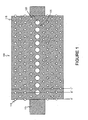
- FIG. 1 shows an xy view of prior art two-dimensional photonic crystal slab apparatus 100.
- Photonic crystal slab 115 has circular holes 110 arranged to from a periodic triangular lattice with a lattice spacing equal to a. Circular holes 110 are filled with air. Region of defects 125 is created by replacing circular holes 110 of the lattice with larger circular holes 120 along a line in the x direction.
- Ridge waveguide 175 couples light into photonic crystal slab apparatus 100 that may have its edge at line A', line B' or line C' in FIG. 1.
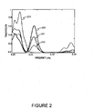
- FIG. 2 shows the transmission coefficient for two-dimensional crystal slab apparatus 100 as a function of frequency expressed in fractions of c/a -where c -is the speed of light -and a is the lattice spacing.
- the radius for circular holes 120 is about 0.45a and the radius for circular holes 110 is about 0.3a.
- Curve 210 represents the unguided case which has low transmission in the bandgap and high transmission in the allow band.
- Curve 201 represents the case where ridge waveguide 175 is attached to photonic crystal slab 115 at the edge defined by line A in FIG. 1.
- Curve 202 represents the case where ridge waveguide 175 is connected to photonic crystal slab 115 at the edge defined by line B in FIG.1.
- Curve 203 represents the case where ridge waveguide 175 is connected to photonic crystal slab 115 at the edge defined by line C' in FIG. 2.
- the transmission for curve 203 is a maximum for a frequency of about 0.253c/a and the waveguide band is narrow.
- Increasing the radius of circular holes 120 to 0.5a causes circular holes 120 to touch and start to overlap. This results in rapid deterioration of the transmission properties of two-dimensional crystal slab apparatus 100 as the light wave becomes less confined due to the decrease of the average dielectric constant of two-dimensional crystal slab 100.
- noncircular holes such as elliptical holes or rectangular holes are introduced as defects in the guiding direction of the photonic-crystal slab to create wide wave guiding bands covering more than 10% of the center frequency portion of the waveguide band.
- the elliptical or rectangular holes form a line of defects in the photonic crystal slab. Because low group velocities occur at the edges of the waveguide bands where the band becomes flat there is a wider range of frequencies with high group velocities available.
- Elliptical and rectangular holes provide significantly wider waveguide bandwidth and higher group velocity than circular holes. Over 10% of guiding bandwidth is achieved for a wide range of elliptical and rectangular shapes. The presence of a wider range of operating frequencies gives more forgiving fabrication tolerance for practical waveguide and allows more design flexibility when stub tuners, add-drop filters, bends and splitters are added. Higher group velocity will also lower the propagation loss of the waveguide.
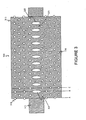
- FIG.3 shows the xy view of typical two-dimensional photonic crystal slab apparatus 300 in an embodiment in accordance with the invention.
- Photonic crystal slab 315 has circular holes 310 arranged to form aperiodic triangular lattice. A periodic honeycomb lattice may also be used.
- Circular holes 310 are etched through photonic crystal slab 315 and are typically filled with a low dielectric constant material such as air. A high dielectric contrast is typically required to open a bandgap in the xy plane.
- region of defects 325 is created by replacing circular holes 310 of the lattice with elliptical holes 320 along a line, for example, in the x direction.
- Elliptical holes 320 are typically filled with the same dielectric material as circular holes 110.
- Ridge waveguide 375 couples light into photonic crystal slab apparatus 300 that may have its edge at line A, line B or line C in FIG. 3.
- FIG. 4 shows an xz cross-sectional view of photonic crystal slab apparatus 300.
- Photonic crystal slab 315 is sandwiched between cladding layer 422 and cladding layer 424.
- cladding layer 422 is positioned between substrate layer 410 and photonic crystal slab 315 (see FIG. 2).
- photonic crystal slab 315 is made from a material having a high dielectric constant compared to air such as silicon or a III-V based semiconductor.
- cladding layers 422 and 424 are typically SiO 2 or other material having a lower dielectric than the material of photonic crystal slab 315.
- Substrate layer 410 is typically of the same material as photonic crystal slab 315 to provide mechanical support but may also be air.
- Layer 412 positioned over cladding layer 424 is typically air.
- Photonic crystal slab apparatus 300 is capable of transmitting light having a frequency that lies within the bandgap of photonic crystal slab 315 in a straight line.
- the waveguide band for photonic crystal slab apparatus 300 depends on a number of factors. Increasing the thickness of photonic crystal slab 315 while keeping all other parameters constant increases the effective dielectric constant and shifts the waveguide band of photonic crystal slab apparatus 300 to lower frequencies. Increasing the cross-section of circular holes 310 while keeping all other parameters constant decreases the effective dielectric constant and shifts the waveguide band of photonic crystal slab apparatus 300 to higher frequencies.
- Increasing the thickness of cladding layers 422 and 424 shifts the position of the waveguide band. If layers 412 and 410 are air, increasing the thickness of cladding layers 422 and 424 slowly moves the position of the waveguide band to lower frequencies and saturates where further increases in thickness produce no further shift in waveguide band position. On the other hand, if layer 410 is not air but, for example, silicon, the position of the waveguide band moves to higher frequencies as cladding layers 422 are increased in thickness and saturates where further increases in thickness produce no further shift in waveguide band position.
- a finite difference time domain method is used to simulate the performance of photonic crystal slab apparatus 300.
- ridge waveguide 375 couples the light into photonic crystal slab 315.
- Photonic crystal slab is taken to have a typical thickness of about 0.6a.
- a complete line of circular holes 310 is removed along the x direction and replaced by elliptical holes 320.
- a dielectric slab of thickness of 0.6 a and dielectric constant of 12.96 is used. The slab is placed on top of a semi-infinite thick material of dielectric constant of 2.
- the ridge waveguide used to couple light to the photonic crystal is 2.28 a wide.
- elliptical holes 320 have semiminor axis of about 0.33a and a semimajor axis of about 0.74a where a is the lattice constant.
- Circular holes 310 have a radius of about 0.3a .
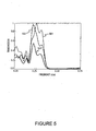
- Curve 501 shows transmission versus frequency for the case where ridge waveguide 375 contacts photonic crystal slab 315 at the left edge defined by line A (see FIG. 3).
- Curve 502 shows transmission versus frequency for the case where ridge waveguide 375 contacts photonic crystal slab 315 at a left edge defined by line B (see FIG. 3).
- Curve 503 shows transmission versus frequency for the case where ridge waveguide 375 contacts photonic crystal slab 315 at a left edge defined by line C (see FIG. 3).
- elliptical holes 320 have a semiminor axis of about 0.37a and a semimajor axis of about 0.738a where a is the lattice constant.
- Circular holes 310 have a radius of about 0.3a.
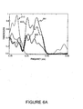
- the width of the waveguide band is about 0.176 of the mid-band frequency.
- Curve 601 shows transmission versus frequency for the case where ridge waveguide 375 contacts photonic crystal slab 315 at the left edge defined by line A (see FIG. 3) and provides a maximum transmission of about 0.89 at the lower edge of the waveguide band.
- Curve 602 shows transmission versus frequency for the case where ridge waveguide 375 contacts photonic crystal slab 315 at a left edge defined by line B (see FIG.
- Curve 603 shows transmission versus frequency for the case where ridge waveguide 375 contacts photonic crystal slab 315 at a left edge defined by line C (see FIG. 3) and provides a maximum transmission of about 0.5. It is apparent from the plots in FIG. 6a that it is not advantageous to couple to photonic crystal slab 315 along an edge defined by line C for the case of elliptical holes 320 having a minor axis of about 0.37a as this typically provides low transmission.
- Coupling ridge waveguide 375 at line B provides a transmission coefficient greater than about 0.5 in the frequency band from about 0.24c/a to about 0.28c/a.
- Coupling ridge waveguide 375 at line A provides a transmission coefficient greater than about 0.5 in the frequency band from about 0.26c/a to about 0.285c/a.
- Coupling ridge waveguide 375 at line C provides a tranmission coefficient of about 0.5 or less for all frequencies of interest as shown by curve 603.
- FIG. 6b shows the negative effect on transmission that occurs when elliptical holes 320 contact and overlap circular holes 310.
- Curve 651 shows the transmission for elliptical holes 320 with a semiminor axis of about 0.39a and a semimajor axis of about 0.872a.
- Curve 652 shows the transmission for elliptical holes 320 with a semiminor axis of about 0.41a and a semimajor axis of about 0.917a. In both cases, elliptical holes 320 contact and overlap circular holes 310. As the overlap between elliptical holes 320 and circular holes 310 increases (as the semiminor axis increases) it is apparent that transmission drops off rapidly due to decreased confinement of the wave.
- FIG. 6c shows the width of the waveguide band over the mid-band frequency versus the semiminor axis in units of the lattice constant, a with the ratio of the major axis to the minor axis fixed at about 2.236 for elliptical holes 320.
- Curve 654 shows that the maximum width of the mid-band frequency is about 0.176.
- FIG. 6d shows the width of the waveguide band over mid-band frequency versus the ratio of the major axis to the minor axis where the semiminor axis is fixed at about 0.37a. Increasing the ratio of the major axis to the minor axis increases the bandwidth as shown by curve 656. In both FIGs. 6c and 6d, after the maximum bandwidth shown is reached, the transmission of photonic crystal slab apparatus 300 will decrease rapidly as elliptical holes 320 begin to overlap with circular holes 310 as indicated, for example, in FIG. 6b.
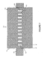
- elliptical holes 320 may be replaced by rectangles 720 to make photonic crystal slab apparatus 700 as shown in FIG. 7.
- Circular holes 710 have a radius of 0.3a.
- FIG. 8a shows transmission versus frequency for ridge waveguide 375 coupled to photonic crystal slab 715 along the edge defined by line B" in FIG. 8a for both curves 812 and 815.
- Curve 812 shows transmission versus frequency for rectangles 720 having a short side of length of about 0.58a and a long side of length about 1.3a.
- Curve 815 shows transmission versus frequency for rectangles 720 having a short side of about 0.62a and a long side of about 1.38a. Transmission for curve 815 is worse because rectangles 720 start to touch and overlap with circular holes 710.
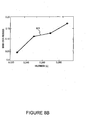
- FIG. 8b shows the width of the waveguide band over mid-frequency versus the half-width of rectangle 720 in units of the lattice constant, a with the ratio of rectangle length to width fixed at about 2.236. As curve 821 shows, the maximum bandwidth is about 0.164.
- FIG. 8c shows the width of the waveguide band over mid-frequency versus the ratio of the length to the width for rectangle 720 and a rectangle halfwidth of about 0.29a.
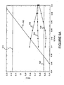
- FIG. 9a shows the band structure for photonic crystal slab apparatus 300 shown in FIG. 3.
- Solid lines 910 and 920 denote the band edges while line 905 marks the boundary of the lightcone.
- line 905 marks the boundary of the lightcone.
- Even mode 939 has low group velocities, however even modes 940 and 939 have higher group velocities.
- FIG. 9b shows the band structure for photonic crystal slab apparatus 700 for rectangles 720 in FIG. 7 having a short side of about 0.58a and a long side of about 1.3a.
- even modes 948 and 949 have an overlap near the frequency of about 0.27c/a which indicates mode mixing is present which is not desirable in single mode applications.
- Even mode 950 is comparable to even mode 940 in FIG. 9a.
- FIG. 9c shows the band structure for photonic crystal slab apparatus 700 with rectangles 720 in FIG. 7 having a short side of about 0.62a and a long side of about 1.38a. Again three even modes 960, 959 and 958 are present. However, transmission is less effective for the configuration in FIG. 9c.
- elliptical holes 320 and rectangular holes 720 provide much wider waveguide bands than do circular holes 120.
- transmission decreases rapidly when there is an overlap between noncircular holes such as elliptical holes 320 or rectangular holes 720.
- Transmission also decreases rapidly when there is an overlap between noncircular holes and circular holes 310 or 710.
- over 10% guiding bandwidth is achieved for a wide range of elliptical and rectangular shapes. Rectangle-like holes with rounded shapes close to neighboring holes also resultsin wide waveguide bands.
- Photonic crystal slab apparatus 300 or photonic crystal slab apparatus 700 may be fabricated in accordance with an embodiment of the invention as shown in FIGs. 10a-10e.
- the initial structure is a silicon on insulator (SOI) structure having silicon layer 1010 and SiO 2 layer 1012 .
- a photonic crystal structure is fabricated in Si layer 1010.
- thin SiO 2 layer 1015 is deposited over Si layer 1010 to serve as a mask layer for subsequent etching of Si layer 1010 as shown in FIG. 10a
- E-beam resist layer 1020 is typically deposited over thin SiO 2 layer 1015 to a typical thickness of about 400 nm as shown in FIG. 10b.
- Resist layer 1020 is patterned to the desired lattice hole pattern using e-beam lithography as shown in FIG.
- thin SiO 2 layer 1015 is etched using reactive ion etching to obtain the desired lattice hole pattern as shown in FIG. 10d.
- the lattice pattern etched in SiO 2 layer 1015 is transferred to Si layer 1010 by a controlled etch typically using HBr shown in 10e: Note that Si layer 1010 is overetched resulting in penetration into SiO 2 layer 1020.
- the completed two-dimensional photonic crystal slab apparatus after the controlled etch is shown in FIG. 10e in a side view.
- Photonic crystal slab apparatus 300 or photonic crystal slab apparatus 700 may be fabricated in accordance with an embodiment of the invention as shown in FIGs. 11a-11f.
- thin SiO 2 layer 1115 is deposited over GaAs layer 1110 to a typical thickness of about 200 nm to serve as a mask layer for subsequent etching of GaAs layer 1110 as shown in FIG. 11 a.
- GaAs layer 1110 is attached to AlGaAs layer 1112.
- E-beam resist layer 1120 is deposited over thin SiO 2 layer 1115 to a typical thickness of about 400 nm as shown in FIG. 11b.
- Resist layer 1120 is patterned to the desired lattice hole pattern using e-beam lithography as shown in FIG. 10c.
- thin SiO 2 layer 1115 is etched using reactive ion etching with CHF 3 to obtain the desired lattice hole pattern as shown in FIG. lid.
- the lattice pattern etched in SiO 2 layer 1115 is transferred to GaAs layer 1110 by a reactive ion etch typically using Cl 2 as shown in FIG. lie.
- a steam oxidation process is then performed of AlGaAs layer 1112 to convert layer 1112 to AlO 2 to obtain the proper refractive index ⁇ 1.5
Landscapes
- Engineering & Computer Science (AREA)
- Physics & Mathematics (AREA)
- Optics & Photonics (AREA)
- Chemical & Material Sciences (AREA)
- Nanotechnology (AREA)
- Microelectronics & Electronic Packaging (AREA)
- General Physics & Mathematics (AREA)
- Life Sciences & Earth Sciences (AREA)
- Biophysics (AREA)
- Crystallography & Structural Chemistry (AREA)
- Optical Integrated Circuits (AREA)
Abstract
Description
Claims (9)
- A two-dimensional photonic crystal slab apparatus (300,700) comprising:a photonic crystal slab (315, 715) comprising a two-dimensional periodic lattice of substantially circular holes (310,710) with a lattice constant;a substantially straight line of defects defining a waveguide in said two-dimensional periodic lattice, said straight line of defects comprising holes (320, 720) having a substantially noncircular cross-section, said holes having a size and arrangement such that said holes do not physically contact said circular holes.
- The apparatus of Claim 1 wherein said substantially circular holes each have a radius that is about 0.3 of said lattice constant.
- The apparatus of Claim 1 or 2 wherein said substantially non-circular cross-section is an ellipse.
- The apparatus of Claim 3 wherein said ellipse (320) has a major axis and a minor axis such that the ratio of said major axis to said minor axis is between about 2 and 2.4.
- The apparatus of Claim 1 or 2 wherein said substantially non-circular cross-section is a rectangle (720).
- The apparatus of one of Claims 1 to 5 wherein said photonic crystal slab (315, 715) is comprised of silicon.
- The apparatus of one of Claims 1 to 6 wherein said two-dimensional periodic lattice is a triangular lattice.
- The apparatus of one of Claims 1 to 7 wherein said circular holes (310,710) are filled with air.
- The apparatus of one of Claims 1 to 5 wherein said photonic crystal slab is comprised of GaAs.
Applications Claiming Priority (2)
| Application Number | Priority Date | Filing Date | Title |
|---|---|---|---|
| US10/192,300 US6728457B2 (en) | 2002-07-10 | 2002-07-10 | Waveguides in two dimensional slab photonic crystals with noncircular holes |
| US192300 | 2002-07-10 |
Publications (3)
| Publication Number | Publication Date |
|---|---|
| EP1380861A2 true EP1380861A2 (en) | 2004-01-14 |
| EP1380861A3 EP1380861A3 (en) | 2005-06-29 |
| EP1380861B1 EP1380861B1 (en) | 2006-07-19 |
Family
ID=29735303
Family Applications (1)
| Application Number | Title | Priority Date | Filing Date |
|---|---|---|---|
| EP03008293A Expired - Lifetime EP1380861B1 (en) | 2002-07-10 | 2003-04-09 | Waveguide in two dimensional slab photonic crystals with noncircular holes |
Country Status (4)
| Country | Link |
|---|---|
| US (2) | US6728457B2 (en) |
| EP (1) | EP1380861B1 (en) |
| JP (1) | JP2004046181A (en) |
| DE (1) | DE60306852T2 (en) |
Cited By (7)
| Publication number | Priority date | Publication date | Assignee | Title |
|---|---|---|---|---|
| US7286738B2 (en) * | 2004-03-25 | 2007-10-23 | Nec Corporation | White light pulse generating method using nonlinear optical device |
| EP2434319A3 (en) * | 2007-01-09 | 2012-05-02 | The Board of Trustees of The Leland Stanford Junior University | Method of fabricating an optical structure on an optical fiber |
| US8331741B2 (en) | 2005-04-29 | 2012-12-11 | The Board Of Trustees Of The Leland Stanford Junior University | Acoustic sensor with at least one photonic crystal structure |
| US8373865B2 (en) | 2006-05-04 | 2013-02-12 | The Board Of Trustees Of The Leland Stanford Junior University | Method of detecting a topology of a reflective surface |
| US8542956B2 (en) | 2010-03-15 | 2013-09-24 | The Board Of Trustees Of The Leland Stanford Junior University | Optical-fiber-compatible acoustic sensor |
| US11215481B2 (en) | 2018-03-23 | 2022-01-04 | The Board Of Trustees Of The Leland Stanford Junior University | Diaphragm-based fiber acoustic sensor |
| US12504320B2 (en) | 2022-04-05 | 2025-12-23 | The Board Of Trustees Of The Leland Stanford Junior University | Self-aligning optical acoustic sensors |
Families Citing this family (26)
| Publication number | Priority date | Publication date | Assignee | Title |
|---|---|---|---|---|
| FR2832513B1 (en) * | 2001-11-21 | 2004-04-09 | Centre Nat Rech Scient | PHOTON CRYSTAL STRUCTURE FOR FASHION CONVERSION |
| AU2003207090A1 (en) * | 2002-02-08 | 2003-09-02 | Matsushita Electric Industrial Co., Ltd. | Semiconductor light-emitting device and its manufacturing method |
| US6728457B2 (en) * | 2002-07-10 | 2004-04-27 | Agilent Technologies, Inc. | Waveguides in two dimensional slab photonic crystals with noncircular holes |
| JP4236092B2 (en) * | 2003-01-31 | 2009-03-11 | Tdk株式会社 | 2D photonic crystal |
| CN100337132C (en) * | 2003-03-26 | 2007-09-12 | Tdk株式会社 | Two-dimensional photonic crystal, and waveguide and resonator using the same |
| WO2005010928A2 (en) * | 2003-07-31 | 2005-02-03 | Anafa Electromagnetic Solutions, Ltd. | Photonic band gap micro-resonator device and method |
| US7418161B2 (en) * | 2004-06-22 | 2008-08-26 | Micron Technology, Inc. | Photonic crystal-based optical elements for integrated circuits and methods therefor |
| JP4297358B2 (en) * | 2004-08-30 | 2009-07-15 | 国立大学法人京都大学 | Two-dimensional photonic crystal and optical device using the same |
| JP3926838B2 (en) * | 2004-11-15 | 2007-06-06 | 松下電器産業株式会社 | Optical waveguide device |
| CN100582656C (en) * | 2006-12-27 | 2010-01-20 | 清华大学 | micro displacement sensor |
| JPWO2009107427A1 (en) * | 2008-02-28 | 2011-06-30 | 日本電気株式会社 | Optical waveguide |
| US7991289B2 (en) * | 2008-03-28 | 2011-08-02 | Raytheon Company | High bandwidth communication system and method |
| CN102931457B (en) * | 2012-11-12 | 2014-09-17 | 中国计量学院 | Round-hole straight-line TeraHertz wave filter |
| US9888283B2 (en) | 2013-03-13 | 2018-02-06 | Nagrastar Llc | Systems and methods for performing transport I/O |
| USD758372S1 (en) | 2013-03-13 | 2016-06-07 | Nagrastar Llc | Smart card interface |
| BR102013018869B1 (en) | 2013-06-25 | 2022-06-07 | Universidade Federal Do Pará | Non-reciprocal divider by three based on a magneto-optical resonator |
| CN104950383B (en) * | 2014-09-29 | 2020-11-13 | 欧阳征标 | Square hole type square lattice photonic crystal low-refractive-index double-compensation scattering column right-angle waveguide |
| CN104950385B (en) * | 2014-09-29 | 2017-01-11 | 欧阳征标 | Square-cylinder-type-square-lattice-photonic-crystal-based high-refractive-index dual-compensation-scattering-cylinder right-angle waveguide |
| CN104950389B (en) * | 2014-09-29 | 2017-01-25 | 欧阳征标 | Cylinder-type-square-lattice-photonic-crystal-based high-refractive-index dual-compensation-scattering-cylinder right-angle waveguide |
| CN104950384B (en) * | 2014-09-29 | 2020-11-13 | 欧阳征标 | Circular hole square lattice photonic crystal low-refractive index double-compensated scattering cylindrical right-angle waveguide |
| CN104597631B (en) * | 2014-09-29 | 2018-09-18 | 欧阳征标 | A kind of three port photocirculator of broadband introducing triangle guide post |
| USD864968S1 (en) | 2015-04-30 | 2019-10-29 | Echostar Technologies L.L.C. | Smart card interface |
| CN105606567A (en) * | 2015-12-04 | 2016-05-25 | 北京邮电大学 | Low-refractive-index-mode one-dimensional photonic crystal nanobeam cavity biosensor structure based on gradual change of elliptical holes |
| CN109789053A (en) * | 2016-08-10 | 2019-05-21 | 汉迪-克拉夫特公司 | Bottle component ventilation insertion piece with siphon component |
| US11968034B2 (en) | 2022-08-18 | 2024-04-23 | X Development Llc | Metastructured photonic devices for binary tree multiplexing or demultiplexing of optical signals |
| CN117148567B (en) * | 2023-06-13 | 2025-02-25 | 天津大学 | A method for optimizing disordered ultra-uniform solid devices based on morphology modification |
Family Cites Families (17)
| Publication number | Priority date | Publication date | Assignee | Title |
|---|---|---|---|---|
| US48422A (en) * | 1865-06-27 | Improved instrument for opening bottles | ||
| US6483640B1 (en) * | 1997-04-08 | 2002-11-19 | The United States Of America As Represented By The Secretary Of The Navy | Optical notch filters based on two-dimensional photonic band-gap materials |
| US6274293B1 (en) * | 1997-05-30 | 2001-08-14 | Iowa State University Research Foundation | Method of manufacturing flexible metallic photonic band gap structures, and structures resulting therefrom |
| JP2001281480A (en) * | 2000-03-29 | 2001-10-10 | Nec Corp | Photonic crystal optical waveguide and directional coupler |
| WO2002014913A1 (en) | 2000-08-15 | 2002-02-21 | Corning Incorporated | Active photonic crystal waveguide device |
| US6674949B2 (en) * | 2000-08-15 | 2004-01-06 | Corning Incorporated | Active photonic crystal waveguide device and method |
| US6593894B1 (en) * | 2000-09-26 | 2003-07-15 | Iowa State University Research Foundation | Highly directional receiver and source antennas using photonic band gap crystals |
| EP1219984B1 (en) * | 2000-12-27 | 2007-07-11 | Nippon Telegraph and Telephone Corporation | Photonic crystal waveguide |
| US6555406B1 (en) * | 2001-02-23 | 2003-04-29 | Iowa State University Research Foundation | Fabrication of photonic band gap materials using microtransfer molded templates |
| US6687447B2 (en) * | 2001-04-30 | 2004-02-03 | Agilent Technologies, Inc. | Stub-tuned photonic crystal waveguide |
| US6560006B2 (en) * | 2001-04-30 | 2003-05-06 | Agilent Technologies, Inc. | Two-dimensional photonic crystal slab waveguide |
| JP3846228B2 (en) * | 2001-06-07 | 2006-11-15 | 日本電気株式会社 | Waveguide |
| US6690876B2 (en) * | 2001-06-27 | 2004-02-10 | Agilent Technologies, Inc. | Three-dimensional photonic crystal waveguide apparatus |
| JP3739328B2 (en) * | 2002-03-13 | 2006-01-25 | 株式会社日立製作所 | Photonic crystal element |
| JP4028751B2 (en) * | 2002-04-24 | 2007-12-26 | 株式会社日立製作所 | Optical waveguide and optical element using the same |
| US6957003B2 (en) * | 2002-06-27 | 2005-10-18 | The Board Of Trustees Of The Leland Stanford Junior University | Creating large bandwidth line defects by embedding dielectric waveguides into photonic crystal slabs |
| US6728457B2 (en) * | 2002-07-10 | 2004-04-27 | Agilent Technologies, Inc. | Waveguides in two dimensional slab photonic crystals with noncircular holes |
-
2002
- 2002-07-10 US US10/192,300 patent/US6728457B2/en not_active Expired - Fee Related
- 2002-10-31 US US10/285,648 patent/US6853791B2/en not_active Expired - Fee Related
-
2003
- 2003-04-09 EP EP03008293A patent/EP1380861B1/en not_active Expired - Lifetime
- 2003-04-09 DE DE60306852T patent/DE60306852T2/en not_active Expired - Lifetime
- 2003-07-01 JP JP2003189235A patent/JP2004046181A/en not_active Withdrawn
Cited By (12)
| Publication number | Priority date | Publication date | Assignee | Title |
|---|---|---|---|---|
| US7286738B2 (en) * | 2004-03-25 | 2007-10-23 | Nec Corporation | White light pulse generating method using nonlinear optical device |
| US8331741B2 (en) | 2005-04-29 | 2012-12-11 | The Board Of Trustees Of The Leland Stanford Junior University | Acoustic sensor with at least one photonic crystal structure |
| US8373865B2 (en) | 2006-05-04 | 2013-02-12 | The Board Of Trustees Of The Leland Stanford Junior University | Method of detecting a topology of a reflective surface |
| US8537368B2 (en) | 2006-05-04 | 2013-09-17 | The Board Of Trustees Of The Leland Stanford Junior University | Method of detecting an acceleration |
| EP2434319A3 (en) * | 2007-01-09 | 2012-05-02 | The Board of Trustees of The Leland Stanford Junior University | Method of fabricating an optical structure on an optical fiber |
| US8548283B2 (en) | 2007-01-09 | 2013-10-01 | The Board Of Trustees Of The Leland Stanford Junior University | Optical system having a photonic crystal structure and method of fabrication |
| US8542956B2 (en) | 2010-03-15 | 2013-09-24 | The Board Of Trustees Of The Leland Stanford Junior University | Optical-fiber-compatible acoustic sensor |
| US8897610B2 (en) | 2010-03-15 | 2014-11-25 | The Board Of Trustees Of The Leland Stanford Junior University | Method of fabricating an optical-fiber-compatible sensor |
| US9702755B2 (en) | 2010-03-15 | 2017-07-11 | The Board Of Trustees Of The Leland Stanford Junior University | Optical-fiber-compatible sensor |
| US11215481B2 (en) | 2018-03-23 | 2022-01-04 | The Board Of Trustees Of The Leland Stanford Junior University | Diaphragm-based fiber acoustic sensor |
| US11629979B2 (en) | 2018-03-23 | 2023-04-18 | The Board Of Trustees Of The Leland Stanford Junior University | Diaphragm-based fiber acoustic sensor |
| US12504320B2 (en) | 2022-04-05 | 2025-12-23 | The Board Of Trustees Of The Leland Stanford Junior University | Self-aligning optical acoustic sensors |
Also Published As
| Publication number | Publication date |
|---|---|
| US6853791B2 (en) | 2005-02-08 |
| DE60306852D1 (en) | 2006-08-31 |
| US6728457B2 (en) | 2004-04-27 |
| JP2004046181A (en) | 2004-02-12 |
| EP1380861B1 (en) | 2006-07-19 |
| US20040008962A1 (en) | 2004-01-15 |
| EP1380861A3 (en) | 2005-06-29 |
| DE60306852T2 (en) | 2007-02-15 |
| US20040008945A1 (en) | 2004-01-15 |
Similar Documents
| Publication | Publication Date | Title |
|---|---|---|
| EP1380861B1 (en) | Waveguide in two dimensional slab photonic crystals with noncircular holes | |
| Chutinan et al. | Diffractionless flow of light in all-optical microchips | |
| EP1255135B1 (en) | Two-dimensional photonic crystal slab and manufacturing method | |
| US8208776B2 (en) | Optical control device | |
| US8094978B2 (en) | Polarization rotator and method for manufacturing the same | |
| EP1219984B1 (en) | Photonic crystal waveguide | |
| US20080152279A1 (en) | Mode transformers for low index high confinement waveguides | |
| JP3800088B2 (en) | Photonic crystal waveguide | |
| Chutinan et al. | Light localization for broadband integrated optics in three dimensions | |
| KR100700751B1 (en) | 2D photonic crystal and waveguide and resonator using it | |
| Kurt et al. | Photonic-crystal heterostructure waveguides | |
| JP2003156642A (en) | Optical waveguide and method of manufacturing the same | |
| JP3876863B2 (en) | Add-drop filter | |
| US6993234B1 (en) | Photonic crystal resonator apparatus with improved out of plane coupling | |
| Shinya et al. | Single-mode transmission in commensurate width-varied line-defect SOI photonic crystal waveguides | |
| US8355614B2 (en) | Optical waveguide | |
| Shinya et al. | Ultrasmall resonant tunneling/dropping devices in 2D photonic crystal slabs | |
| WO2006073194A1 (en) | Optical waveguide, optical device and optical communication device | |
| JP2004101740A (en) | Photonic crystal waveguide | |
| JP4062308B2 (en) | Photonic crystal waveguide | |
| US20090285522A1 (en) | Optical waveguide, optical device, and optical communication device | |
| Lavrinenko et al. | Passive integrated circuits utilizing slow light in photonic crystal waveguides | |
| Shinya et al. | Two-dimensional Si photonic-crystal single-mode waveguide on SOI substrate that operates above the cladding layer light line |
Legal Events
| Date | Code | Title | Description |
|---|---|---|---|
| PUAI | Public reference made under article 153(3) epc to a published international application that has entered the european phase |
Free format text: ORIGINAL CODE: 0009012 |
|
| AK | Designated contracting states |
Kind code of ref document: A2 Designated state(s): AT BE BG CH CY CZ DE DK EE ES FI FR GB GR HU IE IT LI LU MC NL PT RO SE SI SK TR |
|
| AX | Request for extension of the european patent |
Extension state: AL LT LV MK |
|
| PUAL | Search report despatched |
Free format text: ORIGINAL CODE: 0009013 |
|
| AK | Designated contracting states |
Kind code of ref document: A3 Designated state(s): AT BE BG CH CY CZ DE DK EE ES FI FR GB GR HU IE IT LI LU MC NL PT RO SE SI SK TR |
|
| AX | Request for extension of the european patent |
Extension state: AL LT LV MK |
|
| 17P | Request for examination filed |
Effective date: 20051201 |
|
| GRAP | Despatch of communication of intention to grant a patent |
Free format text: ORIGINAL CODE: EPIDOSNIGR1 |
|
| AKX | Designation fees paid |
Designated state(s): DE FR GB |
|
| RTI1 | Title (correction) |
Free format text: WAVEGUIDE IN TWO DIMENSIONAL SLAB PHOTONIC CRYSTALS WITH NONCIRCULAR HOLES |
|
| GRAS | Grant fee paid |
Free format text: ORIGINAL CODE: EPIDOSNIGR3 |
|
| GRAA | (expected) grant |
Free format text: ORIGINAL CODE: 0009210 |
|
| AK | Designated contracting states |
Kind code of ref document: B1 Designated state(s): DE FR GB |
|
| REG | Reference to a national code |
Ref country code: GB Ref legal event code: FG4D |
|
| REG | Reference to a national code |
Ref country code: GB Ref legal event code: 732E |
|
| REF | Corresponds to: |
Ref document number: 60306852 Country of ref document: DE Date of ref document: 20060831 Kind code of ref document: P |
|
| RAP2 | Party data changed (patent owner data changed or rights of a patent transferred) |
Owner name: AVAGO TECHNOLOGIES GENERAL IP (SINGAPORE) PTE. LTD |
|
| ET | Fr: translation filed | ||
| PLBE | No opposition filed within time limit |
Free format text: ORIGINAL CODE: 0009261 |
|
| STAA | Information on the status of an ep patent application or granted ep patent |
Free format text: STATUS: NO OPPOSITION FILED WITHIN TIME LIMIT |
|
| 26N | No opposition filed |
Effective date: 20070420 |
|
| GBPC | Gb: european patent ceased through non-payment of renewal fee |
Effective date: 20070409 |
|
| PG25 | Lapsed in a contracting state [announced via postgrant information from national office to epo] |
Ref country code: GB Free format text: LAPSE BECAUSE OF NON-PAYMENT OF DUE FEES Effective date: 20070409 |
|
| PG25 | Lapsed in a contracting state [announced via postgrant information from national office to epo] |
Ref country code: FR Free format text: LAPSE BECAUSE OF NON-PAYMENT OF DUE FEES Effective date: 20070430 |
|
| PGFP | Annual fee paid to national office [announced via postgrant information from national office to epo] |
Ref country code: DE Payment date: 20110406 Year of fee payment: 9 |
|
| REG | Reference to a national code |
Ref country code: DE Ref legal event code: R119 Ref document number: 60306852 Country of ref document: DE Effective date: 20121101 |
|
| PG25 | Lapsed in a contracting state [announced via postgrant information from national office to epo] |
Ref country code: DE Free format text: LAPSE BECAUSE OF NON-PAYMENT OF DUE FEES Effective date: 20121101 |