EP1378943A1 - Semiconductor device and its manufacturing method - Google Patents
Semiconductor device and its manufacturing method Download PDFInfo
- Publication number
- EP1378943A1 EP1378943A1 EP02707195A EP02707195A EP1378943A1 EP 1378943 A1 EP1378943 A1 EP 1378943A1 EP 02707195 A EP02707195 A EP 02707195A EP 02707195 A EP02707195 A EP 02707195A EP 1378943 A1 EP1378943 A1 EP 1378943A1
- Authority
- EP
- European Patent Office
- Prior art keywords
- region
- semiconductor
- additional
- hetero
- semiconductor layer
- Prior art date
- Legal status (The legal status is an assumption and is not a legal conclusion. Google has not performed a legal analysis and makes no representation as to the accuracy of the status listed.)
- Withdrawn
Links
Images






Classifications
-
- H—ELECTRICITY
- H10—SEMICONDUCTOR DEVICES; ELECTRIC SOLID-STATE DEVICES NOT OTHERWISE PROVIDED FOR
- H10D—INORGANIC ELECTRIC SEMICONDUCTOR DEVICES
- H10D30/00—Field-effect transistors [FET]
- H10D30/80—FETs having rectifying junction gate electrodes
- H10D30/801—FETs having heterojunction gate electrodes
-
- H—ELECTRICITY
- H10—SEMICONDUCTOR DEVICES; ELECTRIC SOLID-STATE DEVICES NOT OTHERWISE PROVIDED FOR
- H10D—INORGANIC ELECTRIC SEMICONDUCTOR DEVICES
- H10D30/00—Field-effect transistors [FET]
- H10D30/60—Insulated-gate field-effect transistors [IGFET]
- H10D30/67—Thin-film transistors [TFT]
- H10D30/674—Thin-film transistors [TFT] characterised by the active materials
- H10D30/6741—Group IV materials, e.g. germanium or silicon carbide
- H10D30/6748—Group IV materials, e.g. germanium or silicon carbide having a multilayer structure or superlattice structure
-
- H—ELECTRICITY
- H10—SEMICONDUCTOR DEVICES; ELECTRIC SOLID-STATE DEVICES NOT OTHERWISE PROVIDED FOR
- H10D—INORGANIC ELECTRIC SEMICONDUCTOR DEVICES
- H10D30/00—Field-effect transistors [FET]
- H10D30/60—Insulated-gate field-effect transistors [IGFET]
- H10D30/751—Insulated-gate field-effect transistors [IGFET] having composition variations in the channel regions
-
- H—ELECTRICITY
- H10—SEMICONDUCTOR DEVICES; ELECTRIC SOLID-STATE DEVICES NOT OTHERWISE PROVIDED FOR
- H10D—INORGANIC ELECTRIC SEMICONDUCTOR DEVICES
- H10D62/00—Semiconductor bodies, or regions thereof, of devices having potential barriers
- H10D62/80—Semiconductor bodies, or regions thereof, of devices having potential barriers characterised by the materials
- H10D62/82—Heterojunctions
- H10D62/822—Heterojunctions comprising only Group IV materials heterojunctions, e.g. Si/Ge heterojunctions
-
- H—ELECTRICITY
- H10—SEMICONDUCTOR DEVICES; ELECTRIC SOLID-STATE DEVICES NOT OTHERWISE PROVIDED FOR
- H10D—INORGANIC ELECTRIC SEMICONDUCTOR DEVICES
- H10D84/00—Integrated devices formed in or on semiconductor substrates that comprise only semiconducting layers, e.g. on Si wafers or on GaAs-on-Si wafers
- H10D84/01—Manufacture or treatment
- H10D84/0123—Integrating together multiple components covered by H10D12/00 or H10D30/00, e.g. integrating multiple IGBTs
- H10D84/0126—Integrating together multiple components covered by H10D12/00 or H10D30/00, e.g. integrating multiple IGBTs the components including insulated gates, e.g. IGFETs
- H10D84/0165—Integrating together multiple components covered by H10D12/00 or H10D30/00, e.g. integrating multiple IGBTs the components including insulated gates, e.g. IGFETs the components including complementary IGFETs, e.g. CMOS devices
- H10D84/0167—Manufacturing their channels
-
- H—ELECTRICITY
- H10—SEMICONDUCTOR DEVICES; ELECTRIC SOLID-STATE DEVICES NOT OTHERWISE PROVIDED FOR
- H10D—INORGANIC ELECTRIC SEMICONDUCTOR DEVICES
- H10D84/00—Integrated devices formed in or on semiconductor substrates that comprise only semiconducting layers, e.g. on Si wafers or on GaAs-on-Si wafers
- H10D84/01—Manufacture or treatment
- H10D84/02—Manufacture or treatment characterised by using material-based technologies
- H10D84/03—Manufacture or treatment characterised by using material-based technologies using Group IV technology, e.g. silicon technology or silicon-carbide [SiC] technology
- H10D84/038—Manufacture or treatment characterised by using material-based technologies using Group IV technology, e.g. silicon technology or silicon-carbide [SiC] technology using silicon technology, e.g. SiGe
Definitions
- the present invention relates to field effect transistors including a heterojunction for a channel region, and more particularly relates to countermeasures against variation in threshold voltage of a field effect transistor.
- the hetero MOS which is a MOS transistor including a semiconductor heterojunction for a channel region
- a semiconductor heterojunction interface is formed at a depth with a small distance apart from the gate insulating film of a semiconductor substrate.
- a channel is formed at the semiconductor heterojunction interface and carriers travel along the channel.
- the semiconductor heterojunction interface is an interface where crystal layers are joined together, and thus energy level at the interface does not fluctuate widely. Therefore, the influence of interface scattering on carriers is small. Accordingly, the hetero MOS has a great current driveability and an excellent characteristic of reduction in noise. Furthermore, the hetero MOS has another characteristic that its threshold voltage can be lower than that of the known MOS transistor.
- the channel region is embedded and therefore threshold voltage largely depends on the thickness of an Si cap region.
- FIG. 15 illustrates the structure of a known hetero MOS.
- the known hetero MOS 100 includes an Si substrate 101 , a gate insulating film 102 formed on the Si substrate 101 , a gate electrode 103 which is formed of polysilicon containing a p-type impurity of high concentration on the gate insulating film 102 , and a sidewall spacer 104 which is formed on the gate insulating film 102 to cover side faces of the gate electrode 103 .
- the Si substrate 101 includes p-type source and drain regions 105 and 106 which are formed on both sides of the gate electrode, an n-type Si cap region 107 formed in a region located between the source and drain regions 105 and 106 , an n-type SiGe channel region 108 formed under the Si cap region, 107 an n-type Si buffer region 109 formed under the SiGe channel region 108 , and an n-type Si body region 110 formed under the Si buffer region 109 .
- FIG. 16 shows the results obtained from simulations of dependency of threshold voltage on the thickness of the Si cap region 107 in the known hetero MOS 100 .
- the absolute value for its threshold voltage remarkably increases.
- the threshold voltage is remarkably increased. This is because as the position at which the channel is formed (i.e., the interface between the Si cap region 107 and the SiGe channel region 108 ) is located a more distance apart from the gate electrode, i.e., further in depth, the potential at the channel changes less enough according to the gate voltage.
- the thickness of the Si cap region 107 is reduced through fabrication processes such as an SiO 2 thermal oxide film formation process and a cleaning process, and thus it is very difficult to control the thickness of the Si cap region 107 . Therefore, nonuniformity in the thickness of the Si cap region 107 can be easily caused. Accordingly, variation in threshold voltage is easily caused and therefore there may be cases where a desired operation can not be performed because of increased threshold voltage.
- the present invention has been contrived in order to solve the foregoing problems and an object of the present invention is to provide a semiconductor device in which an increase in threshold voltage is suppressed.
- a semiconductor device includes: a substrate; a semiconductor layer formed in an upper part of the substrate; a gate insulating film formed on the semiconductor layer; a gate electrode formed on the gate insulating film; first source/drain regions of a first conductivity type formed on both sides of the gate electrode in the semiconductor layer, respectively; a first cap region of the first conductivity type which is formed of a first semiconductor in a region of the semiconductor layer which is located between the first source/drain regions; a first channel region which is formed under the first cap region in the semiconductor layer and formed of a second semiconductor which has a lower potential for carriers at a band edge along which the carriers travel than the corresponding potential of the first semiconductor; and a first body region of a second conductivity type which is formed of a third semiconductor under the first channel region in the semiconductor layer.
- the inventive semiconductor has the structure in which the first cap region of the first conductivity type which is formed of the first semiconductor, the first channel region which is formed under the first cap region and of the second semiconductor in which at a band edge along which the carriers travel than the corresponding potential of the first semiconductor, and the first body region of the second conductivity type which is formed of the third semiconductor under the first channel region in the semiconductor layer. Accordingly, it is possible to achieve a semiconductor device in which an increase in threshold voltage according to an increase in the thickness of the first cap region is suppressed.
- the gate electrode and the first body electrode may be electrically connected to each other.
- the inventive semiconductor device when a gate bias voltage is applied to the gate electrode, forward bias voltage at the same level as the gate bias voltage is applied to the first channel region via the first body region. Therefore, when the gate bias is OFF, the inventive semiconductor device is in the same state as a regular MOS transistor, whereas when the gate bias is ON, the first body region is biased in the forward direction as the gate bias voltage is increased, and thus threshold voltage is reduced. That is to say, a semiconductor device which is operable with a lower threshold voltage can be achieved. Moreover, by forming the semiconductor device in the structure in which the gate electrode and the first body region are electrically connected to each other, the amount of variation in threshold voltage according to nonuniformity in the thickness of the first cap region can be further reduced.
- the inventive semiconductor device has the structure in which the cap region is depleted when a gate bias is applied thereto.
- the concentration of an impurity of the first conductivity contained in the first cap region is 1 ⁇ 10 17 atoms ⁇ cm -3 or more.
- the impurity of the first conductivity type is doped into the first cap region so that at zero bias the potential at a channel which is formed at the interface between the first channel region and the first cap region changes within the range of ⁇ 0.05 eV according to nonuniformity in the thickness of the first cap region.
- the concentration of an impurity of the second conductivity type contained in the first body region is 5 ⁇ 10 18 atoms ⁇ cm -3 or more.
- the body current generated in the lateral parasitic bipolar transistor can be suppressed and kept at a low level. Furthermore, when a voltage is applied to between the source/drain regions, a depletion layer from the source/drain regions can be prevented from expanding. Therefore, even when the concentration of the impurity in the body region is increased, the threshold voltage can be kept at a low level. As a result, the short channel effect that is caused when the gate length is shortened can be prevented.
- the thickness of the first cap region is 10 nm or less.
- the first semiconductor may be silicon.
- the inventive semiconductor device may be formed in the structure in which the second semiconductor is made of silicon and at least one of germanium and carbon.
- the inventive semiconductor device may further include: an additional semiconductor layer formed in an upper part of the substrate; an additional gate insulating film formed on the additional semiconductor layer; an additional gate electrode formed on the additional gate insulating film; additional first source/drain regions of the first conductivity type formed on both sides of the additional gate electrode in the additional semiconductor layer, respectively; an additional first cap region of the first conductivity type which is formed of the first semiconductor in a region of the additional semiconductor layer which is located between the additional first source/drain regions; an additional first channel region which is formed of the second semiconductor under the additional first cap region in the additional semiconductor layer; and an additional first body region of the second conductivity type which is formed of the third semiconductor under the additional first channel region in the additional semiconductor layer.
- the inventive semiconductor device may include: an additional semiconductor layer formed in an upper part of the substrate; an additional gate insulating film formed on the additional semiconductor layer; an additional gate electrode formed on the additional gate insulating film; second source/drain regions of the second conductivity type formed on both sides of the additional gate electrode in the additional semiconductor layer, respectively; a second channel region formed of a fourth semiconductor in a region of the additional semiconductor layer which is located between the second source/drain regions; and a second body region of the first conductivity type which is formed of a fifth semiconductor under the second channel region in the additional semiconductor layer, and the semiconductor device may be formed in the structure that can function as a complementary device.
- the second channel region is of the second conductivity type.
- the gate electrode and the first body region may be electrically connected to each other and the additional gate electrode and the second body region may be electrically connected to each other.
- a method for fabricating a semiconductor device includes the steps of: a) forming in an upper part of a semiconductor substrate a first semiconductor layer including a first semiconductor region into which an impurity of a first conductivity type is doped and a second semiconductor region into which an impurity of a second conductivity type is doped as a complementary device; b) forming on the first semiconductor layer a second semiconductor layer and a third semiconductor layer which is formed of a semiconductor having a wider band gap than the second semiconductor layer; c) forming a mask on part of the third semiconductor layer located in the first semiconductor region, and then introducing an impurity of the first conductivity type into part of the third semiconductor located at least in the second semiconductor region, using the mask; d) removing the mask and then forming a gate insulating film and a gate electrode on part of the third semiconductor layer located in the first semiconductor region and part of the third semiconductor layer located in the second semiconductor region, respectively; and e) forming source/drain regions of the second conductivity type and source/
- the present invention it is possible to achieve a semiconductor device which functions as a complementary device in which variation in threshold voltage in a hetero MIS formed in the second semiconductor region due to nonuniformity in the thickness of the third semiconductor layer that is to be the cap region can be suppressed. Furthermore, according to the present invention, no impurity of the first conductivity type is doped into the part of the third semiconductor layer which is located in the first semiconductor region. Therefore, in a semiconductor device which can be achieved according to the inventive method and functions as a complementary device, characteristics of a hetero MIS formed in the first semiconductor region are not degenerated.
- ions of the impurity of the first conductivity type are implanted so that the peak of the concentration profile of the impurity of the first conductivity type is in the second semiconductor layer or the third semiconductor layer.
- FIG. 1 illustrates the cross-sectional structure of a p-channel hetero MOS 10 of this embodiment in which a SiGe layer is used as a channel region and an Si/SiGe heterojunction is utilized.
- the p-channel hetero MOS 10 of this embodiment includes a p-type Si substrate 11 , a gate insulating film 12 which is formed of an SiO 2 film (having a thickness of about 6 nm) on the Si substrate 11 , a gate electrode 13 which is formed of polysilicon containing a p-type impurity of high concentration on the gate insulating film 12 , and a sidewall spacer 14 which is formed on the gate insulating film 12 to cover the side faces of the gate electrode 13 .
- the p-channel hetero MOS 10 of this embodiment shown in FIG. 1 includes an Si layer 15 , which has been formed in an upper part of the Si substrate 11 by introducing an n-type impurity of high concentration (2 ⁇ 10 18 atoms ⁇ cm -3 ) by ion implantation before crystals are grown in a semiconductor fabrication process.
- an Si layer 16 , an SiGe layer 17 and an Si layer 18 are epitaxially grown in this order by a UHV-CVD method.
- source and drain regions 19 and 20 which contain a p-type impurity of high concentration are formed in regions of the Si layer 15 , the Si layer 16 , the SiGe layer 17 and the Si layer 18 which are located on the sides of the gate electrode 13 .
- a region of the Si layer 15 located between the source and drain regions 19 and 20 is an Si body region 21 containing the n-type impurity of high concentration.
- the Si layer 16 and the SiGe layer 17 are both undoped layers into which no n-type impurity is doped in an as-grown state.
- Regions of the Si layer 16 and the SiGe layer 17 located between the source and drain regions 19 and 20 are an Si buffer region 22 and an SiGe channel region 23 , respectively, which contain the n-type impurity of low concentration.
- a region of the Si film 18 located directly under the gate insulating film 12 is an Si cap region 24 into which a p-type impurity (5 ⁇ 10 17 atoms ⁇ cm -3 ) is introduced.
- the gate insulating film 12 is formed by thermally oxidizing the Si layer 18 .
- a gate bias voltage applied to the gate electrode 13 causes the SiGe channel region 23 and the Si cap region 24 to deplete and holes to travel along the SiGe channel region 23 .
- the thickness of the Si layer 16 is 10 nm and the thickness of the SiGe layer 17 , i.e., the thickness of the SiGe channel region 23 , is 15 nm.
- the Ge content in the SiGe channel region 23 is 30%.
- FIG. 2 shows the correlation between threshold voltage and the thickness of the Si cap region for the known hetero MOS 100 and the hetero MOS 10 ofthis embodiment.
- an n-type impurity is doped into the Si cap region 107 .
- the correlation between threshold voltage and the Si cap region for the known hetero MOS 100 is indicated by the dash-single-dot line (A) shown in FIG. 2 .
- the correlation between threshold voltage and the thickness of the Si cap region is indicated by the solid line (B) shown in FIG. 2 .
- the variation in threshold voltage is small, compared to the known hetero MOS 100 .
- the absolute value for threshold voltage becomes smaller, i.e., the threshold voltage decreases, as the thickness of the Si cap region 24 is increased, as indicated by the broken line (C) in FIG. 2 . This is because the thickness of the Si cap region 24 is increased in the highly doped region and thereby the potential at the SiGe channel region 23 is reduced.
- the thickness of the Si cap region 107 is reduced through an SiO 2 thermal oxide film formation process, a cleaning process and the like during fabrication processes and thus it is very difficult to control the thickness of the Si cap region 107 . Therefore, a difference in the thickness of the Si cap region 107 can be easily caused. This causes variation in threshold voltage even in a wafer and among identical wafers, which has been a big problem of the known hetero MOS.
- FIGS. 3(a) through 3(c) are graphs illustrating the band profiles at zero bias for three types of hetero MOS devices having the impurity profiles used in the simulations of FIG. 2 .
- FIGS. 3(a) through 3(c) each illustrate four different band profiles in the respective cases where the thickness of the Si cap region 24 is 1 nm, 2 nm, 5 nm, or 10 nm.
- the absolute value for the potential at the valance band in the SiGe channel region 23 increases as the thickness of the Si cap region 24 is increased. This causes an increase in threshold voltage.
- the potential at the valence band in the SiGe channel region 23 (the convex upward slope segment in FIG. 3(b) ) is kept almost constant and the potential at an edge of the valence band around the interface between the SiGe channel region 23 and the Si cap region 24 changes within the range of ⁇ 0.05 eV. That is to say, variation in threshold voltage is suppressed.
- the absolute value for the potential at the valence band in the SiGe channel region 23 reduces as the thickness of the Si cap region 24 is increased. This reduction corresponds to the reduction in threshold voltage indicated by the broken line in FIG. 2 .
- the concentration of an impurity to be doped can be set such that the potential at the SiGe channel region 23 is kept almost constant.
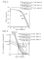
- FIG. 4 shows the results obtained from simulations of the Vg-Id characteristics of the three types of hetero MOS devices shown in FIGS. 2 and 3 .
- the thicknesses of the Si cap region 24 and the Si cap region 107 are both 5 nm.
- a predetermined drain current can flow at a lower gate voltage than in the known hetero MOS 100 indicated by the dash-single-dot line (A). Furthermore, when the concentration of the p-type impurity that is doped into the Si cap region 24 is increased, a predetermined drain current can flow at a further lower gate voltage as indicated by the broken line (C).
- the hetero MOS 10 of this embodiment in which the p-type impurity is doped into the Si cap region 24 can achieve the effect that threshold voltage can be lower than that in the known hetero MOS 100 .
- the concentration of the p-type impurity contained in the Si cap region 24 need only be 1 ⁇ 10 17 atoms ⁇ cm -3 or more.
- the concentration of the p-type impurity contained in the Si cap region 24 is preferably 1 ⁇ 10 18 atoms ⁇ cm -3 or less.
- FIG. 5 is a graph on which peaks of the concentration of holes which are stored around the interface between the gate insulating film 12 (SiO 2 and the Si cap region 24 (i.e., parasitic channel) and the interface between the Si cap region 24 and the SiGe channel region 23 (i.e., channel) by applying a gate voltage are plotted against the gate voltage.
- the range in which the number of holes stored around the interface between the Si cap region 24 and the SiGe channel region 23 is larger than that of holes stored around the parasitic channel is indicated by the voltage range A of FIG. 5 .
- the hetero MOS 10 of this embodiment including the Si cap region 24 into which the p-type impurity is doped
- the range in which the number of holes stored around the interface between the Si cap region 24 and the SiGe channel region 23 is larger than that of holes stored around the parasitic channel expands to the voltage range B and to the voltage range C in this order as the concentration of the p-type impurity is increased to 5 ⁇ 10 17 atoms ⁇ cm -3 (indicated by the solid line (B)) and then to 1 ⁇ 10 18 atoms ⁇ cm -3 (indicated by the broken line (C)).
- the thickness of the Si cap region 24 of each of the hetero MOS devices 10 does not change widely in order to further reduce variation in threshold voltage among the hetero MOS devices 10 . More specifically, the range of differences in the thickness of the Si cap region 24 is preferably 10 nm or less.
- the threshold voltage in the hetero MOS can be also reduced. Furthermore, the parasitic channel in question in the known hetero MOS can be suppressed, resulting in a high drive current.
- the present invention is not limited thereto. Similar effects can be gained also in any n-channel hetero MOS devices into which are introduced respective impurities of opposite conductivity types to those of the p-channel hetero MOS. That is to say, as long as a hetero MOS has a structure in which an impurity whose conductivity is the same as that of carriers traveling along a channel is properly doped into a semiconductor layer (which corresponds to the Si cap region 24 of this embodiment) which exists between a channel region and a gate insulating film to form a heterojunction with the channel region, variation in threshold voltage in the hetero MOS can be suppressed.
- a channel region formed of Si 1-x C x instead of the SiGe channel region 23 , and an Si cap region into which an n-type impurity is doped may be used to form an n-channel hetero MOS.
- SiGeC may be used as a channel to form an n-channel hetero MOS using an Si cap region into which an n-type impurity is doped or to form a p-channel hetero MOS using an Si cap region into which a p-type impurity is doped.
- these MOS devices may be integrated to form a CMOS.
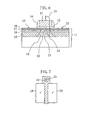
- FIG. 6 illustrates a cross-sectional structure of a p-channel hetero DTMOS 60 using a SiGe layer as a channel region and utilizing an Si/SiGe heterojunction according to this embodiment.
- FIG. 7 is a top view of the p-channel hetero DTMOS 60 .
- the p-channel hetero DTMOS 60 of this embodiment includes a p-type Si substrate 11 , a gate insulating film 12 which is formed of an SiO 2 film (having a thickness of about 6 nm) on the Si substrate 11 , a gate electrode 13 which is formed of polysilicon containing a p-type impurity of high concentration on the gate insulating film 12 , and a sidewall spacer 14 which is formed on the gate insulating film 12 to cover the side faces of the gate electrode 13 .
- the p-channel hetero DTMOS 60 of this embodiment shown in FIG. 6 includes an Si layer 15 , which has been formed in an upper part of the Si substrate 11 by introducing an n-type impurity at a high concentration (2 ⁇ 10 18 atoms ⁇ cm -3 ) by ion implantation before crystals are grown in a semiconductor fabrication process.
- an Si layer 16 , an SiGe layer 17 and an Si layer 18 are epitaxially grown in this order by a UHV-CVD method.
- source and drain regions 19 and 20 that contain a p-type impurity of high concentration are formed in regions of the Si layer 15 , the Si layer 16 , the SiGe layer 17 and the Si layer 18 which are located on both sides of the gate electrode 13 .
- a region of the Si layer 15 located between the source and drain regions 19 and 20 is an Si body region 21 which contains the n-type impurity of high concentration.
- the Si body region 21 and the gate electrode 13 are electrically connected to each other by an interconnect 25 .
- the gate electrode 13 and the Si body region 21 are directly connected to each other outside of the region in which a channel is to be formed.
- the Si layer 16 and the SiGe layer 17 are both undoped layers into which no n-type impurity is doped in an as-grown state. Regions of the Si layer 16 and the SiGe layer 17 located between the source and drain regions 19 and 20 are an Si buffer region 22 and an SiGe channel region 23 , respectively, which contain the n-type impurity of low concentration. A region of the Si film 18 located directly under the gate insulating film 12 is an Si cap region 24 into which a p-type impurity (5 ⁇ 10 17 atoms ⁇ cm -3 ) is introduced. The gate insulating film 12 is formed by thermally oxidizing the Si layer 18 . When the p-channel hetero MOS 10 of this embodiment is in operation, a gate bias voltage applied to the gate electrode 13 causes the SiGe channel region 23 and the Si cap region 24 to deplete and holes to travel along the SiGe channel region 23 .
- the thickness of the Si layer 16 is 10 nm and the thickness of the SiGe layer 17 , i.e., the thickness of the SiGe channel region 23 , is 15 nm.
- the Ge content in the SiGe channel region 23 is 30%.
- the hetero DTMOS of this embodiment has basically the same structure as the hetero MOS described in Embodiment 1.
- the hetero DTMOS of this embodiment is different from the hetero MOS in that the gate electrode 13 and the Si body region 21 are electrically connected to each other.
- the gate electrode 13 and the Si body region 21 are electrically connected to each other. Because of this, when a gate bias voltage is applied to the gate electrode 13 , a forward bias voltage at the same level as the gate bias voltage is applied to the Si channel region 23 via the Si body region 21 . Therefore, when the gate bias is OFF, the hetero DTMOS is in the same state as a regular MOS transistor, whereas when the gate bias is ON, the Si body region 21 is biased in the forward direction as the gate bias voltage is increased, and thus threshold voltage is reduced. Accordingly, the hetero DTMOS of this embodiment is operable with a lower threshold voltage, compared to DTMOS using a known Si substrate.
- the substrate bias coefficient ⁇ can be set at a large value, the threshold voltage is largely reduced during operation and the effective gate overdrive is increased. As a result, a high ON current can be obtained. That is to say, according to the hetero DTMOS 60 of this embodiment, great current driveability and high speed switching can be achieved even at a low voltage.
- FIG. 8 shows the correlation between threshold voltage and the thickness of the Si cap region for a hetero DTMOS which is obtained by electrically connecting the gate electrode 13 and the Si body region 21 in the known hetero MOS 100 (which will be hereinafter referred to a "known hetero DTMOS") and for the hetero DTMOS 60 of this embodiment in which the p-type impurity is introduced into the Si cap region 24 .
- known hetero DTMOS the known hetero MOS 100
- the n-type impurity is doped into the Si cap region 107 .
- the correlation between threshold voltage and the thickness of the Si cap region is indicated by the dash-single-dot line (a) in FIG. 8 .
- the correlation between the threshold voltage and the thickness of the Si cap region 24 for the hetero DTMOS 60 of this embodiment including the Si cap region 24 into which a p-type impurity at about 5 ⁇ 10 17 atoms ⁇ cm -3 is doped is indicated by the solid line (b) in FIG. 8 .
- the variation in threshold voltage is smaller than that in the known hetero DTMOS.
- the concentration of the p-type impurity in the Si cap region 24 i.e., where the concentration of the p-type impurity is 1 ⁇ 10 18 atoms ⁇ cm -3 as indicated by the broken line (c) in FIG.
- the absolute value for threshold voltage becomes smaller as the thickness of the Si cap region 24 is increased, in contrast to the known hetero DTMOS (indicated by the dash-single-dot line (a)). In other words, the threshold voltage is reduced. This is because the thickness of the Si cap region 24 is increased in the highly doped region and thereby the potential at the SiGe channel region 23 decreases.
- the amount of the variation in the threshold voltage in this embodiment is smaller than in the hetero MOS 10 of Embodiment 1.
- the hetero DTMOS 60 of this embodiment is more effective to stabilize threshold voltage than the hetero MOS 10 of Embodiment 1.
- the concentration of the p-type impurity contained in the Si cap region 24 need only be 1 ⁇ 10 17 atoms ⁇ cm -3 or more.
- the concentration of the p-type impurity contained in the Si cap region 24 is preferably 1 ⁇ 10 18 atoms ⁇ cm -3 or less.
- FIG. 9 shows the results obtained from simulations of the Vg-Id characteristics for the known hetero DTMOS, and the hetero DTMOS 60 of this embodiment in which the p-type impurity is introduced into the Si cap region 24 .
- the thicknesses of the Si cap region 107 of the known hetero DTMOS and the Si cap region 24 of the hetero DTMOS 60 are both 5 nm.
- a lateral parasitic bipolar transistor is generated through a p-type gate, an n-type body (base), a p-type source region 19 (emitter) and a drain region 20 (collector).
- base n-type body
- emitter p-type source region 19
- drain region 20 collector
- FIG. 10 is a graph showing the Vg-Id characteristics of each of the known hetero DTMOS (the concentration of the n-type impurity in the body region 21 : 2 ⁇ 10 18 atoms ⁇ cm -3 ) and the hetero DTMOS 60 of this embodiment, where the concentration of the n-type impurity in the Si body region 21 of the hetero DTMOS 60 of this embodiment is set at a higher level (2 ⁇ 10 19 atoms ⁇ cm -3 ) so that the threshold voltage of the hetero DTMOS 60 is equal to that of the known hetero DTMOS.
- the p-type impurity is doped into the Si cap region 24 and thereby the threshold voltage is reduced.
- the concentration of the impurity in the body region 21 can be set a higher level in accordance with the reduction in threshold voltage.
- concentration of the impurity in the body region 21 is increased, a built-in potential is increased between the source and the body. Accordingly, the body current generated in the lateral parasitic bipolar transistor can be kept at a low level. That is to say, the operation voltage range can be enlarged.
- a depletion layer from the source region 19 and the drain region 20 can be prevented from expanding.
- the concentration of the impurity in the body region 21 is set at 2 ⁇ 10 19 atoms ⁇ cm -3 .
- similar effects can be achieved as long as the concentration is 5 ⁇ 10 18 atoms ⁇ cm -3 or more.
- nonuniformity in the thickness of the Si cap region 24 can be suppressed. Accordingly, even if nonuniformity in the thickness of the Si cap region 24 occurs because of fluctuation in a fabrication process and a difference between fabrication processes, variation in threshold voltage in a wafer, among wafers, and among lots can be reduced.
- nonuniformity in the thickness of the Si cap regions 24 of the hetero DTMOS devices 60 are not so wide. More specifically, the range of nonuniformity in the thickness of the Si cap regions 24 is preferably 10 nm or less.
- the threshold voltage can be reduced by properly doping a p-type impurity into the Si cap region 24 .
- the body current in question in the hetero DTMOS structure can be suppressed, and thereby a wide range of operation voltage can be achieved. Accordingly, the short channel effect can be sufficiently suppressed.
- the present invention is not limited to such a structure. Similar effects can be gained also in any n-channel hetero MOS devices into which are introduced respective impurities of the opposite conductivity types to those of the p-channel hetero DTMOS. That is to say, as long as a hetero DTMOS has a structure in which an impurity whose conductivity is the same as that of carriers traveling along a channel is properly doped into a semiconductor layer (corresponding to the Si cap region 24 of this embodiment) which exists between a channel region and a gate insulating film to form a heterojunction with the channel region, it is possible to achieve a hetero DTMOS in which variation in threshold voltage is suppressed.
- a channel region formed of Si 1-x C x instead of the SiGe channel region 23 , and an Si cap region into which the n-type impurity is doped may be used to form an n-channel hetero DTMOS.
- SiGeC may be used as a channel to form an n-channel hetero DTMOS using an Si cap region into which the n-type impurity is doped or to form a p-channel hetero MOS using an Si cap region into which a p-type impurity is doped.
- these MOS devices may be integrated to form a complementary DTMOS.
- FIG. 11 illustrates a cross-sectional structure of the complementary hetero MOS 70 of this embodiment using an SiGe layer as a channel region and utilizing an Si/SiGe heterojunction.
- the complementary hetero MOS 70 of this embodiment includes an Si layer 15a , an embedded oxide layer 15b which is formed by implanting oxygen ions into the Si layer 15a or like methods, a semiconductor layer 30 for a p-channel hetero MOS (hereinafter referred to a "p-hetero MOS”) which is formed on the embedded oxide film 15b , and a semiconductor layer 90 for an n-channel hetero MOS (hereinafter referred to an "n-hetero MOS”) which is formed on the embedded oxide film 15b .
- p-hetero MOS a p-channel hetero MOS
- n-hetero MOS n-channel hetero MOS
- a gate insulating film 12 which is formed of an SiO 2 film (having a thickness of about 6 nm), a gate electrode 13 which is formed of polysilicon containing a p-type impurity of high concentration on the gate insulating film 12 , and a sidewall spacer 14 which is formed on the gate insulating film 12 to cover the side faces of the gate electrode 13 are provided.
- an n-type impurity of high concentration (2 ⁇ 10 18 atoms ⁇ cm -3 ) is introduced into the semiconductor layer 30 for the p-hetero MOS by ion implantation before crystals are grown, and thereby an Si layer 15 is formed.
- an Si layer 16 , an SiGe layer 17 and an Si layer 18 are epitaxitially grown in this order by an UHV-CVD method.
- source and drain regions 19 and 20 which contain the p-type impurity of high concentration are formed in regions of the Si layer 15 , the Si layer 16 , the SiGe layer 17 and the Si layer 18 which are located on both sides of the gate electrode 13 .
- a region of the Si layer 15 located between the source region 19 and the drain region 20 is an Si body region 21 which contains the n-type impurity of high concentration.
- the Si layer 16 and the SiGe layer 17 are both undoped layers into which no n-type impurity is doped in an as-grown state.
- Regions of the Si layer 16 and the SiGe layer 17 located between the source and drain regions 19 and 20 are an Si buffer region 22 and an SiGe channel region 23 , respectively, which contain the n-type impurity of low concentration.
- a region of the Si film 18 located directly under the gate insulating film 12 is an Si cap region 24 into which a p-type impurity (5 ⁇ 10 17 atoms ⁇ cm -3 ) is introduced.
- the gate insulating film 12 is formed by thermally oxidizing the Si layer 18 .
- a p-type impurity of high concentration (2 ⁇ 10 18 atoms ⁇ cm -3 ) is introduced into the semiconductor layer 90 for the n-hetero MOS at a high concentration by ion implantation before crystals are grown, and thereby an Si layer 75 is formed.
- an Si layer 76 , an SiGe layer 77 and an Si layer 78 are epitaxitially grown in this order by a UHV-CVD method.
- source and drain regions 79 and 80 which contain the n-type impurity of high concentration are formed in regions of the Si layer 75 , the Si layer 76 , the SiGe layer 77 and the Si layer 78 which are located on both sides of the gate electrode 73 .
- a region of the Si layer 75 located between the source region 79 and the drain region 80 is an Si body region 81 which contains the p-type impurity of high concentration.
- the Si layer 76 and the SiGe layer 77 are both undoped layers into which no p-type impurity is doped in an as-grown state.
- Regions of the Si layer 76 and the SiGe layer 77 located between the source and drain regions 79 and 80 are an Si buffer region 82 and an SiGe channel region 83 , respectively, which contain the p-type impurity of low concentration.
- a region of the Si film 78 located directly under the gate insulating film 72 is an Si channel region 84 .
- the Si channel region 84 of the n-type hetero MOS of this embodiment is an undoped layer into which no impurity is doped in an as-grown state.
- the thicknesses of the Si layers 16 and 76 are both 10 nm and the thicknesses of the SiGe layers 17 and 77 , i.e., the thicknesses of the SiGe channel region 23 and the SiGe region 83 , are both 15 nm.
- the Ge contents in the SiGe channel region 23 and the SiGe region 83 are both 30%.
- the complementary hetero MOS 70 of this embodiment includes: the p-hetero MOS which is formed on an SOI substrate and has the almost same structure as the hetero MOS 10 of Embodiment 1 ; and the n-hetero MOS which is formed on the SOI substrate and has the almost same structure as the hetero MOS 10 of Embodiment 1 but is different from the hetero MOS 10 in that the conductivity type of each member is opposite to that of the corresponding member of the hetero MOS 10 . Furthermore, in the n-hetero MOS, the p-type impurity is not doped into the Si channel region 84 .
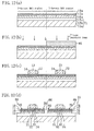
- FIG. 12 illustrates cross-sectional views showing process steps of the method of this embodiment for fabricating the complementary hetero MOS 70 .
- an SOI substrate 71 formed of an Si layer 15a , an embedded oxide film 15b and an Si layer 15c is prepared.
- an n + Si region i.e., a p-hetero MOS region
- a p + Si region i.e., an n-hetero MOS region
- an Si layer 16a , an SiGe layer 17a , an Si layer 18a are epitaxially grown on the Si layer 15c in this order by a UHV-CVD method.
- each of the layers is an undoped layer and the layers are formed so that the respective thicknesses of the Si layer 16a , the SiGe layer 17a , the Si layer 18a are 10 nm, 15 nm, and 5 nm and that the Ge content in the SiGe layer 17a is 30%.
- a resist mask is deposited on the n-hetero MOS region. Thereafter, a p-type impurity is doped into part of the Si layer 18a which is located in the p-hetero MOS region at a concentration of about 5 ⁇ 10 17 atoms ⁇ cm - 3 by ion implantation using the resist mask as a mask.
- the resist mask is removed and then the gate insulating films 12 and 72 are formed on parts of the Si layer 18a which are in the p-hetero MOS region and the n-hetero MOS region, respectively.
- an n + gate electrode 13 formed of polysilicon, into which an n-type impurity of high concentration is doped, and a p + gate electrode 73 formed of polysilicon, into which a p-type impurity of high concentration is doped, are formed on the insulating films 12 and 72 , respectively.
- sidewall spacers 14 and 74 are formed to cover the side faces of the gate electrodes 13 and 73 .
- impurity ions are implanted at a high concentration using each of the gate electrodes and the sidewall spacers as a mask, thereby forming n + type source and drain regions 19 and 20 and p + type source and drain regions 79 and 80 .
- a trench 86 is formed to isolate the p-hetero MOS region from the n-hetero MOS region.
- an Si layer 15 , an Si layer 16 , an SiGe layer 17 and an Si layer 18 are formed in the p-hetero MOS region whereas an Si layer 75 , an Si layer 76 , an SiGe layer 77 and an Si layer 78 are formed in the n-hetero MOS region.
- an Si body region 21 In the region between the source and drain regions 19 and 20 , an Si body region 21 , an Si buffer region 22 , an SiGe channel region 23 and an Si cap region 24 are formed. In the region between the source and drain regions 79 and 80 , an Si body region 81 , an Si buffer region 82 , an SiGe region 83 and an Si channel region 84 are formed.
- the complementary hetero MOS 70 can be obtained.
- CMOS device using a high-performance hetero MOS can be fabricated in a simple manner.
- a gate electrode and an Si body region may be electrically connected to each other by a contact in each of the p-hetero MOS and the n-hetero MOS to form a complementary hetero DTMOS.
- the Si cap region 24 of the p-hetero MOS by properly introducing a p-type impurity into the Si cap region 24 of the p-hetero MOS, variation in threshold voltage in a hetero MOS due to nonuniformity in the thickness of the Si cap region 24 can be suppressed. Accordingly, even if nonuniformity in the thickness of the Si cap region 24 occurs because of fluctuation in a fabrication process or between the fabrication processes, variation in threshold voltage in a wafer, among wafers, and among lots can be reduced. It is also possible to reduce the threshold voltage in the p-hetero MOS. Furthermore, the parasitic channel in question in the known hetero MOS can be suppressed, and thus a high drive current can be achieved.
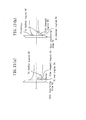
- FIG. 13(a) shows band profiles of the p-hetero MOS included in the complementary hetero MOS 70 of this embodiment when gate bias voltage is applied thereto and FIG. 13(b) shows band profiles of the n-hetero MOS included in the complementary hetero MOS 70 of this embodiment when the gate bias voltage is applied thereto.
- a channel is formed in the SiGe channel region 23 and holes travel along the channel.
- a channel is formed in the Si channel region 84 and electrons travel along the channel.
- the p-type impurity is introduced into the Si layer 18a by in-situ doping in the process step shown in FIG. 12(a)
- an Si layer 78 into which the p-type impurity is doped is formed at the end. Because of this, the valence band in the Si channel region 84 has such a potential as indicated by the broken line in FIG. 13(b) and, as a result, threshold voltage is increased.
- the p-type impurity is not introduced by in-situ doping but by ion implantation into only the part of the Si layer 18a which is located in the p-hetero MOS region.
- the valence band in the Si channel region 84 has such a potential as one indicated by the solid line in FIG. 13(b) . Therefore, the increase in threshold voltage in the n-hetero MOS is suppressed and thus the characteristics of the n-hetero MOS are hardly degenerated.
- FIG. 14 shows the Ge contents and the impurity profiles in the Si body region 21 , the Si buffer region 22 , the SiGe channel region 23 and the Si cap region 24 of the p-hetero MOS included in the complementary hetero MOS of this embodiment.
- the concentration of the p-type impurity is the highest (5 ⁇ 10 17 atoms ⁇ cm -3 ) at the surface of the Si cap region 24 and the concentration is reduced with increasing depth from the surface.
- the Si cap region 24 is formed through introduction of a p-type impurity by ion implantation according to the method for fabricating the complementary hetero MOS of this embodiment and thus there may be cases where the p-type impurity reaches a region located directly under the Si cap region 24 . If the p-type impurity reaches the region located directly under the cap region 24 , a region through which holes travel may be formed, besides the interface between the Si cap region 24 and the SiGe channel region 23 , in a region located at a greater depth from the surface of the Si cap region 24 (e.g., in the Si buffer region 22 ). Therefore, it is difficult to control the drain current to be ON/OFF by gate bias voltage that is applied to the gate electrode 13 . In other words, the characteristics of the p-hetero MOS are degenerated.
- the concentration of the p-type impurity is set at the highest level in the Si cap region 24 or the SiGe channel region 23 (i.e., to put the peak of the p-type impurity profile in the Si cap region 24 or the SiGe channel region 23 ).
- the concentration of the p-type impurity is the highest in the Si cap region 24 . It is further preferable that the concentration of the p-type impurity is the highest at the surface of the Si cap region 24 .
- a complementary hetero MOS including a high-performance p-hetero MOS can be obtained without the characteristics of an n-hetero MOS being degenerated.
- the present invention can be utilized for field effective transistors, such as heterojunction MOS transistors and hetero junction DTMOS transistors, including a heterojunction for a channel region.
Landscapes
- Insulated Gate Type Field-Effect Transistor (AREA)
- Thin Film Transistor (AREA)
- Metal-Oxide And Bipolar Metal-Oxide Semiconductor Integrated Circuits (AREA)
Abstract
A region of an Si layer 15 located between source and drain regions 19 and 20 is
an Si body region 21 which contains an n-type impurity of high concentration. An Si
layer 16 and an SiGe layer 17 are, in an as grown state, undoped layers into which no n-type
impurity is doped. Regions of the Si layer 16 and the SiGe layer 17 located between
the source and drain regions 19 and 20 are an Si buffer region 22 and an SiGe channel
region 23, respectively, which contain the n-type impurity of low concentration. A region
of an Si film 18 located directly under a gate insulating film 12 is an Si cap region 24 into
which a p-type impurity (5 × 10¹⁷ atoms·cm-3) is doped. Accordingly, a semiconductor
device in which an increase in threshold voltage is suppressed can be achieved.
Description
The present invention relates to field effect transistors including a heterojunction
for a channel region, and more particularly relates to countermeasures against variation in
threshold voltage of a field effect transistor.
In recent years, portable communication terminals represented by cellular phones
are widely used. Such portable terminals are generally driven by batteries and it is
strongly desired to reduce power consumption without sacrificing operation speed in
portable terminals in order to prolong the lifetime of batteries. To achieve a portable
communication terminal with low power consumption without reducing operation speed, it
is effective to increase drain saturation current to maintain current driveability while
lowering threshold voltage to reduce supply voltage in the portable terminal. To satisfy
such demands, there have been many studies on heterojunction MOS transistors (which
will be hereinafter called "hetero MOS") using as a channel region a material with high-mobility
carriers.
In a known MOS transistor, carriers travel along the interface between a gate
oxide film and a silicon substrate. Energy level largely fluctuates around the interface
between the gate oxide film that is an amorphous layer and the silicon substrate that is a
crystal layer. Because of the energy level fluctuation, carriers are easily affected by
interface scattering in the known MOS transistor, resulting in problems such as reduction
of carrier mobility and increase in noise.
On the other hand, in the hetero MOS, which is a MOS transistor including a
semiconductor heterojunction for a channel region, a semiconductor heterojunction
interface is formed at a depth with a small distance apart from the gate insulating film of a
semiconductor substrate. A channel is formed at the semiconductor heterojunction
interface and carriers travel along the channel. The semiconductor heterojunction
interface is an interface where crystal layers are joined together, and thus energy level at
the interface does not fluctuate widely. Therefore, the influence of interface scattering on
carriers is small. Accordingly, the hetero MOS has a great current driveability and an
excellent characteristic of reduction in noise. Furthermore, the hetero MOS has another
characteristic that its threshold voltage can be lower than that of the known MOS
transistor.
However, in the hetero MOS including a heterojunction for a channel region, the
channel region is embedded and therefore threshold voltage largely depends on the
thickness of an Si cap region.
FIG. 15 illustrates the structure of a known hetero MOS.
As shown in FIG. 15, the known hetero MOS 100 includes an Si substrate 101, a
gate insulating film 102 formed on the Si substrate 101, a gate electrode 103 which is
formed of polysilicon containing a p-type impurity of high concentration on the gate
insulating film 102, and a sidewall spacer 104 which is formed on the gate insulating film
102 to cover side faces of the gate electrode 103. The Si substrate 101 includes p-type
source and drain regions 105 and 106 which are formed on both sides of the gate electrode,
an n-type Si cap region 107 formed in a region located between the source and drain
regions 105 and 106, an n-type SiGe channel region 108 formed under the Si cap region,
107 an n-type Si buffer region 109 formed under the SiGe channel region 108, and an n-type
Si body region 110 formed under the Si buffer region 109.
FIG. 16 shows the results obtained from simulations of dependency of threshold
voltage on the thickness of the Si cap region 107 in the known hetero MOS 100.
As shown in FIG. 16, as the thickness of the Si cap region 107 is increased, the
absolute value for its threshold voltage remarkably increases. In other words, the
threshold voltage is remarkably increased. This is because as the position at which the
channel is formed (i.e., the interface between the Si cap region 107 and the SiGe channel
region 108) is located a more distance apart from the gate electrode, i.e., further in depth,
the potential at the channel changes less enough according to the gate voltage.
In terms of processing, however, the thickness of the Si cap region 107 is reduced
through fabrication processes such as an SiO2 thermal oxide film formation process and a
cleaning process, and thus it is very difficult to control the thickness of the Si cap region
107. Therefore, nonuniformity in the thickness of the Si cap region 107 can be easily
caused. Accordingly, variation in threshold voltage is easily caused and therefore there
may be cases where a desired operation can not be performed because of increased
threshold voltage.
Particularly, in an integrated circuit including a plural number of identical
transistors, variation in threshold voltage among the transistors causes gaps of switching
time among the transistors. As a result, the timing gaps among the transistors in the
integrated circuit occur, so that the integrated circuit may not operate properly. Moreover,
under consideration of variation in threshold voltage among the transistors, in order to
ensure an operation margin, the latest switching timing should be set as a standard timing
and therefore it is difficult to increase in operation speed of the integrated circuit.
The present invention has been contrived in order to solve the foregoing problems
and an object of the present invention is to provide a semiconductor device in which an
increase in threshold voltage is suppressed.
A semiconductor device according to the present invention includes: a substrate; a
semiconductor layer formed in an upper part of the substrate; a gate insulating film formed
on the semiconductor layer; a gate electrode formed on the gate insulating film; first
source/drain regions of a first conductivity type formed on both sides of the gate electrode
in the semiconductor layer, respectively; a first cap region of the first conductivity type
which is formed of a first semiconductor in a region of the semiconductor layer which is
located between the first source/drain regions; a first channel region which is formed under
the first cap region in the semiconductor layer and formed of a second semiconductor
which has a lower potential for carriers at a band edge along which the carriers travel than
the corresponding potential of the first semiconductor; and a first body region of a second
conductivity type which is formed of a third semiconductor under the first channel region
in the semiconductor layer.
The inventive semiconductor has the structure in which the first cap region of the
first conductivity type which is formed of the first semiconductor, the first channel region
which is formed under the first cap region and of the second semiconductor in which at a
band edge along which the carriers travel than the corresponding potential of the first
semiconductor, and the first body region of the second conductivity type which is formed
of the third semiconductor under the first channel region in the semiconductor layer.
Accordingly, it is possible to achieve a semiconductor device in which an increase in
threshold voltage according to an increase in the thickness of the first cap region is
suppressed.
The gate electrode and the first body electrode may be electrically connected to
each other.
Accordingly, when a gate bias voltage is applied to the gate electrode, forward
bias voltage at the same level as the gate bias voltage is applied to the first channel region
via the first body region. Therefore, when the gate bias is OFF, the inventive
semiconductor device is in the same state as a regular MOS transistor, whereas when the
gate bias is ON, the first body region is biased in the forward direction as the gate bias
voltage is increased, and thus threshold voltage is reduced. That is to say, a
semiconductor device which is operable with a lower threshold voltage can be achieved.
Moreover, by forming the semiconductor device in the structure in which the gate
electrode and the first body region are electrically connected to each other, the amount of
variation in threshold voltage according to nonuniformity in the thickness of the first cap
region can be further reduced.
The inventive semiconductor device has the structure in which the cap region is
depleted when a gate bias is applied thereto.
It is preferable that the concentration of an impurity of the first conductivity
contained in the first cap region is 1 × 10¹⁷ atoms·cm-3 or more.
It is preferable that the impurity of the first conductivity type is doped into the
first cap region so that at zero bias the potential at a channel which is formed at the
interface between the first channel region and the first cap region changes within the range
of ±0.05 eV according to nonuniformity in the thickness of the first cap region.
Accordingly, it is possible to achieve a semiconductor device in which variation
in threshold voltage is suppressed even if nonuniformity in the thickness of the cap region
occurs.
It is preferable that the concentration of an impurity of the second conductivity
type contained in the first body region is 5 × 10¹⁸ atoms·cm-3 or more.
Accordingly, the body current generated in the lateral parasitic bipolar transistor
can be suppressed and kept at a low level. Furthermore, when a voltage is applied to
between the source/drain regions, a depletion layer from the source/drain regions can be
prevented from expanding. Therefore, even when the concentration of the impurity in the
body region is increased, the threshold voltage can be kept at a low level. As a result, the
short channel effect that is caused when the gate length is shortened can be prevented.
It is preferable that the thickness of the first cap region is 10 nm or less.
The first semiconductor may be silicon.
The inventive semiconductor device may be formed in the structure in which the
second semiconductor is made of silicon and at least one of germanium and carbon.
The inventive semiconductor device may further include: an additional
semiconductor layer formed in an upper part of the substrate; an additional gate insulating
film formed on the additional semiconductor layer; an additional gate electrode formed on
the additional gate insulating film; additional first source/drain regions of the first
conductivity type formed on both sides of the additional gate electrode in the additional
semiconductor layer, respectively; an additional first cap region of the first conductivity
type which is formed of the first semiconductor in a region of the additional semiconductor
layer which is located between the additional first source/drain regions; an additional first
channel region which is formed of the second semiconductor under the additional first cap
region in the additional semiconductor layer; and an additional first body region of the
second conductivity type which is formed of the third semiconductor under the additional
first channel region in the additional semiconductor layer.
Accordingly, even if nonuniformity in the thickness of the first cap region is
caused in a fabrication process or between fabrication processes, it is possible to achieve a
semiconductor device in which variation in threshold voltage between transistors is
suppressed.
The inventive semiconductor device may include: an additional semiconductor
layer formed in an upper part of the substrate; an additional gate insulating film formed on
the additional semiconductor layer; an additional gate electrode formed on the additional
gate insulating film; second source/drain regions of the second conductivity type formed
on both sides of the additional gate electrode in the additional semiconductor layer,
respectively; a second channel region formed of a fourth semiconductor in a region of the
additional semiconductor layer which is located between the second source/drain regions;
and a second body region of the first conductivity type which is formed of a fifth
semiconductor under the second channel region in the additional semiconductor layer, and
the semiconductor device may be formed in the structure that can function as a
complementary device.
It is preferable that the second channel region is of the second conductivity type.
Accordingly, variation in threshold voltage in a transistor formed on the additional
semiconductor layer can be suppressed.
The gate electrode and the first body region may be electrically connected to each
other and the additional gate electrode and the second body region may be electrically
connected to each other.
A method for fabricating a semiconductor device according to the present
invention includes the steps of: a) forming in an upper part of a semiconductor substrate a
first semiconductor layer including a first semiconductor region into which an impurity of
a first conductivity type is doped and a second semiconductor region into which an
impurity of a second conductivity type is doped as a complementary device; b) forming on
the first semiconductor layer a second semiconductor layer and a third semiconductor layer
which is formed of a semiconductor having a wider band gap than the second
semiconductor layer; c) forming a mask on part of the third semiconductor layer located in
the first semiconductor region, and then introducing an impurity of the first conductivity
type into part of the third semiconductor located at least in the second semiconductor
region, using the mask; d) removing the mask and then forming a gate insulating film and a
gate electrode on part of the third semiconductor layer located in the first semiconductor
region and part of the third semiconductor layer located in the second semiconductor
region, respectively; and e) forming source/drain regions of the second conductivity type
and source/drain regions of the first conductivity type in the first semiconductor region and
in the second semiconductor region, respectively, by implanting ions of respective
impurities into the first, second and third semiconductor layers using each of the gate
electrodes as a mask.
According to the present invention, it is possible to achieve a semiconductor
device which functions as a complementary device in which variation in threshold voltage
in a hetero MIS formed in the second semiconductor region due to nonuniformity in the
thickness of the third semiconductor layer that is to be the cap region can be suppressed.
Furthermore, according to the present invention, no impurity of the first conductivity type
is doped into the part of the third semiconductor layer which is located in the first
semiconductor region. Therefore, in a semiconductor device which can be achieved
according to the inventive method and functions as a complementary device,
characteristics of a hetero MIS formed in the first semiconductor region are not
degenerated.
It is preferable that in the step c), ions of the impurity of the first conductivity type
are implanted so that the peak of the concentration profile of the impurity of the first
conductivity type is in the second semiconductor layer or the third semiconductor layer.
Accordingly, variation in threshold voltage in a transistor formed in the first
semiconductor region can be suppressed.
Hereinafter, embodiments of the present invention will be described with
reference to the accompanying drawings. For the sake of simplicity, components
common to the embodiments are identified by the same reference numerals.
First, the structure of a hetero MOS in accordance with this embodiment will be
described. FIG. 1 illustrates the cross-sectional structure of a p-channel hetero MOS 10
of this embodiment in which a SiGe layer is used as a channel region and an Si/SiGe
heterojunction is utilized.
As shown in FIG. 1, the p-channel hetero MOS 10 of this embodiment includes a p-type
Si substrate 11, a gate insulating film 12 which is formed of an SiO2 film (having a
thickness of about 6 nm) on the Si substrate 11, a gate electrode 13 which is formed of
polysilicon containing a p-type impurity of high concentration on the gate insulating film
12, and a sidewall spacer 14 which is formed on the gate insulating film 12 to cover the
side faces of the gate electrode 13.
The p-channel hetero MOS 10 of this embodiment shown in FIG. 1 includes an Si
layer 15, which has been formed in an upper part of the Si substrate 11 by introducing an
n-type impurity of high concentration (2 × 10¹⁸ atoms·cm-3) by ion implantation before
crystals are grown in a semiconductor fabrication process. On the Si layer 15, an Si layer
16, an SiGe layer 17 and an Si layer 18 are epitaxially grown in this order by a UHV-CVD
method.
Furthermore, in the p-channel hetero MOS 10 of this embodiment, source and drain
regions 19 and 20 which contain a p-type impurity of high concentration are formed in
regions of the Si layer 15, the Si layer 16, the SiGe layer 17 and the Si layer 18 which are
located on the sides of the gate electrode 13.
A region of the Si layer 15 located between the source and drain regions 19 and 20
is an Si body region 21 containing the n-type impurity of high concentration. The Si
layer 16 and the SiGe layer 17 are both undoped layers into which no n-type impurity is
doped in an as-grown state. Regions of the Si layer 16 and the SiGe layer 17 located
between the source and drain regions 19 and 20 are an Si buffer region 22 and an SiGe
channel region 23, respectively, which contain the n-type impurity of low concentration.
A region of the Si film 18 located directly under the gate insulating film 12 is an Si cap
region 24 into which a p-type impurity (5 × 10¹⁷ atoms·cm-3) is introduced. The gate
insulating film 12 is formed by thermally oxidizing the Si layer 18. When the p-channel
hetero MOS 10 of this embodiment is in operation, a gate bias voltage applied to the gate
electrode 13 causes the SiGe channel region 23 and the Si cap region 24 to deplete and
holes to travel along the SiGe channel region 23.
The thickness of the Si layer 16 is 10 nm and the thickness of the SiGe layer 17,
i.e., the thickness of the SiGe channel region 23, is 15 nm. The Ge content in the SiGe
channel region 23 is 30%.
FIG. 2 shows the correlation between threshold voltage and the thickness of the Si
cap region for the known hetero MOS 100 and the hetero MOS 10 ofthis embodiment.
In the known hetero MOS 100, an n-type impurity is doped into the Si cap region
107. The correlation between threshold voltage and the Si cap region for the known
hetero MOS 100 is indicated by the dash-single-dot line (A) shown in FIG. 2.
On the other hand, as for the hetero MOS 10 of this embodiment including the Si
cap region 24 into which the p-type impurity is doped at a concentration of about 5 × 10¹⁷
atoms·cm-3, the correlation between threshold voltage and the thickness of the Si cap
region is indicated by the solid line (B) shown in FIG. 2. As can be seen from FIG. 2, as
for the hetero MOS 10 of this embodiment, the variation in threshold voltage is small,
compared to the known hetero MOS 100. Furthermore, at an increased concentration of
the p-type impurity in the Si cap region 24 (i.e., a concentration of the p-type impurity of 1
× 1018 atoms·cm-3), in contrast to the known hetero MOS 100, the absolute value for
threshold voltage becomes smaller, i.e., the threshold voltage decreases, as the thickness of
the Si cap region 24 is increased, as indicated by the broken line (C) in FIG. 2. This is
because the thickness of the Si cap region 24 is increased in the highly doped region and
thereby the potential at the SiGe channel region 23 is reduced.
Accordingly, by doping a p-type impurity into the Si cap region 24, an increase in
threshold voltage can be suppressed even when the thickness of the Si cap region 24 is
increased because of fluctuation in a fabrication process and a difference between
fabrication processes.
As for the known hetero MOS 100, the thickness of the Si cap region 107 is
reduced through an SiO2 thermal oxide film formation process, a cleaning process and the
like during fabrication processes and thus it is very difficult to control the thickness of the
Si cap region 107. Therefore, a difference in the thickness of the Si cap region 107 can be
easily caused. This causes variation in threshold voltage even in a wafer and among
identical wafers, which has been a big problem of the known hetero MOS.
According to this embodiment, however, by properly doping a p-type impurity
into the Si cap region 24, variation in threshold voltage can be suppressed even if a
difference in the thickness of the Si cap region 24 occurs between fabrication processes.
Further description of how the variation in threshold voltage can be suppressed will be
made with reference to FIG. 3.
FIGS. 3(a) through 3(c) are graphs illustrating the band profiles at zero bias for
three types of hetero MOS devices having the impurity profiles used in the simulations of
FIG. 2. FIGS. 3(a) through 3(c) each illustrate four different band profiles in the
respective cases where the thickness of the Si cap region 24 is 1 nm, 2 nm, 5 nm, or 10 nm.
As shown in FIG. 3(a), in the known hetero MOS 100, the absolute value for the
potential at the valance band in the SiGe channel region 23 (the convex upward slope
segment in FIG. 3(a)) increases as the thickness of the Si cap region 24 is increased. This
causes an increase in threshold voltage.
On the other hand, as shown in FIG. 3(b), in the hetero MOS 10 of this
embodiment in which the p-type impurity at about 5 × 10¹⁷ atoms·cm-3 is doped into the Si
cap region 24, even if nonuniformity in the thickness of the Si cap region 24 occur, the
potential at the valence band in the SiGe channel region 23 (the convex upward slope
segment in FIG. 3(b)) is kept almost constant and the potential at an edge of the valence
band around the interface between the SiGe channel region 23 and the Si cap region 24
changes within the range of ±0.05 eV. That is to say, variation in threshold voltage is
suppressed.
Furthermore, when the concentration of the p-type impurity that is doped into the
Si cap region 24 is increased, as shown in FIG. 3(c), the absolute value for the potential at
the valence band in the SiGe channel region 23 (the convex upward slope segment in FIG.
3(c)) reduces as the thickness of the Si cap region 24 is increased. This reduction
corresponds to the reduction in threshold voltage indicated by the broken line in FIG. 2.
From the foregoing description, it can be understood that in order to suppress
variation in threshold voltage due to nonuniformity in the thickness of the Si cap region 24,
the concentration of an impurity to be doped can be set such that the potential at the SiGe
channel region 23 is kept almost constant.
Next, the Vg-Id characteristics of the three types of hetero MOS devices each
including a Si cap region of a different impurity concentration will be shown in FIG. 4.
FIG. 4 shows the results obtained from simulations of the Vg-Id characteristics of the three
types of hetero MOS devices shown in FIGS. 2 and 3. In this case, the thicknesses of the
Si cap region 24 and the Si cap region 107 are both 5 nm.
As shown in FIG. 4, in the hetero MOS 10 of this embodiment indicated by the
solid line (B) in which the p-type impurity at about 5 × 10¹⁷ atoms·cm-3 is doped into the Si
cap region 24, a predetermined drain current can flow at a lower gate voltage than in the
known hetero MOS 100 indicated by the dash-single-dot line (A). Furthermore, when the
concentration of the p-type impurity that is doped into the Si cap region 24 is increased, a
predetermined drain current can flow at a further lower gate voltage as indicated by the
broken line (C).
As can be understood from the foregoing description, the hetero MOS 10 of this
embodiment in which the p-type impurity is doped into the Si cap region 24 can achieve
the effect that threshold voltage can be lower than that in the known hetero MOS 100. In
order to suppress variation in threshold voltage in a hetero MOS due to nonuniformity in
the thickness of the Si cap region 24, the concentration of the p-type impurity contained in
the Si cap region 24 need only be 1 × 10¹⁷ atoms·cm-3 or more. Furthermore, the
concentration of the p-type impurity contained in the Si cap region 24 is preferably 1 × 10¹⁸
atoms·cm-3 or less. This is because a great effect of suppressing variation in threshold
voltage in the hetero MOS due to nonuniformity in the thickness of the Si cap region 24
can be gained within the range of the p-type impurity described above, as shown in FIGS.
2 and 3.
FIG. 5 is a graph on which peaks of the concentration of holes which are stored
around the interface between the gate insulating film 12 (SiO2 and the Si cap region 24
(i.e., parasitic channel) and the interface between the Si cap region 24 and the SiGe
channel region 23 (i.e., channel) by applying a gate voltage are plotted against the gate
voltage.
As shown in FIG. 5, in the known hetero MOS 100 (indicated by the dash-single-dot
line (A)) including the Si cap region 107 into which the n-type impurity is doped (at a
concentration of 1 × 10¹⁷ atoms·cm-3), the range in which the number of holes stored
around the interface between the Si cap region 24 and the SiGe channel region 23 is larger
than that of holes stored around the parasitic channel is indicated by the voltage range A of
FIG. 5. On the other hand, in the hetero MOS 10 of this embodiment including the Si cap
region 24 into which the p-type impurity is doped, it can be understood that the range in
which the number of holes stored around the interface between the Si cap region 24 and the
SiGe channel region 23 is larger than that of holes stored around the parasitic channel
expands to the voltage range B and to the voltage range C in this order as the concentration
of the p-type impurity is increased to 5 × 10¹⁷ atoms·cm-3 (indicated by the solid line (B))
and then to 1 × 10¹⁸ atoms·cm-3 (indicated by the broken line (C)). This shows that the
parasitic channel in question in the known hetero MOS 100 can be suppressed, resulting in
a high drive current.
As has been described, by properly introducing a p-type impurity into the Si cap
region 24, variation in threshold voltage in the hetero MOS due to nonuniformity in the
thickness of the Si cap region 24 can be suppressed. Accordingly, even if nonuniformity
in the thickness of the Si cap region 24 occurs because fluctuation in a fabrication process
and a difference between the fabrication processes, variation in threshold voltage in a
wafer, among wafers, and among lots can be reduced. Specifically, in the case of
fabricating an integrated circuit using a plurality of the hetero MOS devices 10 of this
embodiment, it is preferable that the thickness of the Si cap region 24 of each of the hetero
MOS devices 10 does not change widely in order to further reduce variation in threshold
voltage among the hetero MOS devices 10. More specifically, the range of differences in
the thickness of the Si cap region 24 is preferably 10 nm or less.
The threshold voltage in the hetero MOS can be also reduced. Furthermore, the
parasitic channel in question in the known hetero MOS can be suppressed, resulting in a
high drive current.
Although the p-channel hetero MOS using the SiGe channel region 23 has been
described in this embodiment, the present invention is not limited thereto. Similar effects
can be gained also in any n-channel hetero MOS devices into which are introduced
respective impurities of opposite conductivity types to those of the p-channel hetero MOS.
That is to say, as long as a hetero MOS has a structure in which an impurity whose
conductivity is the same as that of carriers traveling along a channel is properly doped into
a semiconductor layer (which corresponds to the Si cap region 24 of this embodiment)
which exists between a channel region and a gate insulating film to form a heterojunction
with the channel region, variation in threshold voltage in the hetero MOS can be
suppressed. For example, a channel region formed of Si1-xCx, instead of the SiGe channel
region 23, and an Si cap region into which an n-type impurity is doped may be used to
form an n-channel hetero MOS. Alternatively, SiGeC may be used as a channel to form
an n-channel hetero MOS using an Si cap region into which an n-type impurity is doped or
to form a p-channel hetero MOS using an Si cap region into which a p-type impurity is
doped. Furthermore, these MOS devices may be integrated to form a CMOS.
Next, the structure of a hetero DTMOS in accordance with this embodiment will
be described. FIG. 6 illustrates a cross-sectional structure of a p-channel hetero DTMOS
60 using a SiGe layer as a channel region and utilizing an Si/SiGe heterojunction according
to this embodiment. FIG. 7 is a top view of the p-channel hetero DTMOS 60.
As shown in FIG. 6, the p-channel hetero DTMOS 60 of this embodiment includes
a p-type Si substrate 11, a gate insulating film 12 which is formed of an SiO2 film (having a
thickness of about 6 nm) on the Si substrate 11, a gate electrode 13 which is formed of
polysilicon containing a p-type impurity of high concentration on the gate insulating film
12, and a sidewall spacer 14 which is formed on the gate insulating film 12 to cover the
side faces of the gate electrode 13.
The p-channel hetero DTMOS 60 of this embodiment shown in FIG. 6 includes an
Si layer 15, which has been formed in an upper part of the Si substrate 11 by introducing
an n-type impurity at a high concentration (2 × 10¹⁸ atoms·cm-3) by ion implantation before
crystals are grown in a semiconductor fabrication process. On the Si layer 15, an Si layer
16, an SiGe layer 17 and an Si layer 18 are epitaxially grown in this order by a UHV-CVD
method.
Furthermore, in the p-channel hetero DTMOS 60 of this embodiment, source and
drain regions 19 and 20 that contain a p-type impurity of high concentration are formed in
regions of the Si layer 15, the Si layer 16, the SiGe layer 17 and the Si layer 18 which are
located on both sides of the gate electrode 13.
A region of the Si layer 15 located between the source and drain regions 19 and 20,
is an Si body region 21 which contains the n-type impurity of high concentration. The Si
body region 21 and the gate electrode 13 are electrically connected to each other by an
interconnect 25. Specifically, as shown in FIG. 7, the gate electrode 13 and the Si body
region 21 are directly connected to each other outside of the region in which a channel is to
be formed.
The Si layer 16 and the SiGe layer 17 are both undoped layers into which no n-type
impurity is doped in an as-grown state. Regions of the Si layer 16 and the SiGe layer 17
located between the source and drain regions 19 and 20 are an Si buffer region 22 and an
SiGe channel region 23, respectively, which contain the n-type impurity of low
concentration. A region of the Si film 18 located directly under the gate insulating film
12 is an Si cap region 24 into which a p-type impurity (5 × 10¹⁷ atoms·cm-3) is introduced.
The gate insulating film 12 is formed by thermally oxidizing the Si layer 18. When the p-channel
hetero MOS 10 of this embodiment is in operation, a gate bias voltage applied to
the gate electrode 13 causes the SiGe channel region 23 and the Si cap region 24 to deplete
and holes to travel along the SiGe channel region 23.
The thickness of the Si layer 16 is 10 nm and the thickness of the SiGe layer 17,
i.e., the thickness of the SiGe channel region 23, is 15 nm. The Ge content in the SiGe
channel region 23 is 30%.
As can be understood from the foregoing description, the hetero DTMOS of this
embodiment has basically the same structure as the hetero MOS described in Embodiment
1. However, the hetero DTMOS of this embodiment is different from the hetero MOS in
that the gate electrode 13 and the Si body region 21 are electrically connected to each
other.
In the hetero DTMOS 60 of this embodiment, as shown in FIG. 6, the gate
electrode 13 and the Si body region 21 are electrically connected to each other. Because
of this, when a gate bias voltage is applied to the gate electrode 13, a forward bias voltage
at the same level as the gate bias voltage is applied to the Si channel region 23 via the Si
body region 21. Therefore, when the gate bias is OFF, the hetero DTMOS is in the same
state as a regular MOS transistor, whereas when the gate bias is ON, the Si body region 21
is biased in the forward direction as the gate bias voltage is increased, and thus threshold
voltage is reduced. Accordingly, the hetero DTMOS of this embodiment is operable with
a lower threshold voltage, compared to DTMOS using a known Si substrate.
Furthermore, in the hetero DTMOS 60 of this embodiment, since the substrate
bias coefficient γ can be set at a large value, the threshold voltage is largely reduced during
operation and the effective gate overdrive is increased. As a result, a high ON current can
be obtained. That is to say, according to the hetero DTMOS 60 of this embodiment, great
current driveability and high speed switching can be achieved even at a low voltage.
FIG. 8 shows the correlation between threshold voltage and the thickness of the Si
cap region for a hetero DTMOS which is obtained by electrically connecting the gate
electrode 13 and the Si body region 21 in the known hetero MOS 100 (which will be
hereinafter referred to a "known hetero DTMOS") and for the hetero DTMOS 60 of this
embodiment in which the p-type impurity is introduced into the Si cap region 24.
In the known hetero DTMOS, the n-type impurity is doped into the Si cap region
107. The correlation between threshold voltage and the thickness of the Si cap region is
indicated by the dash-single-dot line (a) in FIG. 8.
On the other hand, the correlation between the threshold voltage and the thickness
of the Si cap region 24 for the hetero DTMOS 60 of this embodiment including the Si cap
region 24 into which a p-type impurity at about 5×10¹⁷ atoms·cm-3 is doped is indicated by
the solid line (b) in FIG. 8. As can be seen from FIG. 8, in the hetero DTMOS 60 of this
embodiment, the variation in threshold voltage is smaller than that in the known hetero
DTMOS. Furthermore, at an increased concentration of the p-type impurity in the Si cap
region 24 (i.e., where the concentration of the p-type impurity is 1 × 10¹⁸ atoms·cm-3 as
indicated by the broken line (c) in FIG. 8), the absolute value for threshold voltage
becomes smaller as the thickness of the Si cap region 24 is increased, in contrast to the
known hetero DTMOS (indicated by the dash-single-dot line (a)). In other words, the
threshold voltage is reduced. This is because the thickness of the Si cap region 24 is
increased in the highly doped region and thereby the potential at the SiGe channel region
23 decreases.
Furthermore, the amount of the variation in the threshold voltage in this
embodiment is smaller than in the hetero MOS 10 of Embodiment 1. This shows that the
hetero DTMOS 60 of this embodiment is more effective to stabilize threshold voltage than
the hetero MOS 10 of Embodiment 1. In order to suppress variation in threshold voltage
in the hetero DTMOS due to nonuniformity in the thickness of the Si cap region 24, the
concentration of the p-type impurity contained in the Si cap region 24 need only be 1 × 10¹⁷
atoms·cm-3 or more. Furthermore, the concentration of the p-type impurity contained in
the Si cap region 24 is preferably 1 × 10¹⁸ atoms·cm-3 or less. This is because a great
effect of suppressing variation in threshold voltage in the hetero MOS due to
nonuniformity in the thickness of the Si cap region 24 can be gained within the range of
the concentration of the p-type impurity described above, as shown in FIG. 8.
FIG. 9 shows the results obtained from simulations of the Vg-Id characteristics for
the known hetero DTMOS, and the hetero DTMOS 60 of this embodiment in which the p-type
impurity is introduced into the Si cap region 24. In this case, the thicknesses of the
Si cap region 107 of the known hetero DTMOS and the Si cap region 24 of the hetero
DTMOS 60 are both 5 nm.
Referring to FIG. 9, when the results for the known hetero DTMOS indicated by
the dash-single-dot line (a) and the hetero DTMOS 60 ofthis embodiment indicated by the
solid line (b) are compared, it can be understood that the threshold voltage can be reduced.
In a DTMOS, in general, a lateral parasitic bipolar transistor is generated through
a p-type gate, an n-type body (base), a p-type source region 19 (emitter) and a drain region
20 (collector). When the transistor turns on and body current flows, the body current
might practically become a problem.
Referring to FIG. 9, however, no difference in the body current is shown between
the known hetero DTMOS and the hetero DTMOS 60 ofthis embodiment. That is to say,
in the hetero DTMOS 60 of this embodiment, the difference between the body and drain
currents is enlarged, so that the operation voltage range that is controlled by the body
current can be enlarged.
FIG. 10 is a graph showing the Vg-Id characteristics of each of the known hetero
DTMOS (the concentration of the n-type impurity in the body region 21: 2 × 10¹⁸
atoms·cm-3) and the hetero DTMOS 60 of this embodiment, where the concentration of the
n-type impurity in the Si body region 21 of the hetero DTMOS 60 of this embodiment is
set at a higher level (2 × 10¹⁹ atoms·cm-3) so that the threshold voltage of the hetero
DTMOS 60 is equal to that of the known hetero DTMOS.
According to this embodiment, the p-type impurity is doped into the Si cap region
24 and thereby the threshold voltage is reduced. The concentration of the impurity in the
body region 21 can be set a higher level in accordance with the reduction in threshold
voltage. When the concentration of the impurity in the body region 21 is increased, a
built-in potential is increased between the source and the body. Accordingly, the body
current generated in the lateral parasitic bipolar transistor can be kept at a low level. That
is to say, the operation voltage range can be enlarged. Furthermore, at an increased
concentration of the impurity in the body region 21, when a voltage is applied to between
the source and the drain, a depletion layer from the source region 19 and the drain region
20 can be prevented from expanding. Therefore, even when the concentration of the
impurity in the body region is increased, the threshold voltage can be kept at a low level
and the short channel effect that is caused when the gate length is shortened can be
prevented. In this embodiment, the concentration of the impurity in the body region 21 is
set at 2 × 10¹⁹ atoms·cm-3. However, similar effects can be achieved as long as the
concentration is 5 × 10¹⁸atoms·cm-3 or more.
As has been described, by properly doping a p-type impurity into the Si cap
region 24, variation in threshold voltage due to nonuniformity in the thickness of the Si cap
region can be suppressed. Accordingly, even if nonuniformity in the thickness of the Si
cap region 24 occurs because of fluctuation in a fabrication process and a difference
between fabrication processes, variation in threshold voltage in a wafer, among wafers, and
among lots can be reduced. Specifically, in fabricating an integrated circuit using a
plurality of the hetero DTMOS devices 20 of this embodiment, in order to further suppress
variation in threshold voltage among the hetero MOS devices 60, it is preferable that
nonuniformity in the thickness of the Si cap regions 24 of the hetero DTMOS devices 60
are not so wide. More specifically, the range of nonuniformity in the thickness of the Si
cap regions 24 is preferably 10 nm or less.
Also, the threshold voltage can be reduced by properly doping a p-type impurity
into the Si cap region 24.
Moreover, the body current in question in the hetero DTMOS structure can be
suppressed, and thereby a wide range of operation voltage can be achieved. Accordingly,
the short channel effect can be sufficiently suppressed.
Although the p-channel hetero DTMOS using the SiGe channel region 23 has
been described in this embodiment, the present invention is not limited to such a structure.
Similar effects can be gained also in any n-channel hetero MOS devices into which are
introduced respective impurities of the opposite conductivity types to those of the p-channel
hetero DTMOS. That is to say, as long as a hetero DTMOS has a structure in
which an impurity whose conductivity is the same as that of carriers traveling along a
channel is properly doped into a semiconductor layer (corresponding to the Si cap region
24 of this embodiment) which exists between a channel region and a gate insulating film to
form a heterojunction with the channel region, it is possible to achieve a hetero DTMOS in
which variation in threshold voltage is suppressed. For example, a channel region formed
of Si1-xCx, instead of the SiGe channel region 23, and an Si cap region into which the n-type
impurity is doped may be used to form an n-channel hetero DTMOS. Moreover,
SiGeC may be used as a channel to form an n-channel hetero DTMOS using an Si cap
region into which the n-type impurity is doped or to form a p-channel hetero MOS using an
Si cap region into which a p-type impurity is doped. Furthermore, these MOS devices
may be integrated to form a complementary DTMOS.
According to this embodiment, the structure of a complementary hetero MOS will
be described. FIG. 11 illustrates a cross-sectional structure of the complementary hetero
MOS 70 of this embodiment using an SiGe layer as a channel region and utilizing an
Si/SiGe heterojunction.
As shown in FIG. 11, the complementary hetero MOS 70 of this embodiment
includes an Si layer 15a, an embedded oxide layer 15b which is formed by implanting
oxygen ions into the Si layer 15a or like methods, a semiconductor layer 30 for a p-channel
hetero MOS (hereinafter referred to a "p-hetero MOS") which is formed on the embedded
oxide film 15b, and a semiconductor layer 90 for an n-channel hetero MOS (hereinafter
referred to an "n-hetero MOS") which is formed on the embedded oxide film 15b. On the
semiconductor layer 30, a gate insulating film 12 which is formed of an SiO2 film (having
a thickness of about 6 nm), a gate electrode 13 which is formed of polysilicon containing a
p-type impurity of high concentration on the gate insulating film 12, and a sidewall spacer
14 which is formed on the gate insulating film 12 to cover the side faces of the gate
electrode 13 are provided. On the semiconductor layer 90, a gate insulating film 72
formed of an SiO2 film (having a thickness of about 6 nm), a gate electrode 73 which is
formed of polysilicon containing an n-type impurity of high concentration on the gate
insulating film 72, and a sidewall spacer 74 which is formed on the gate insulating film 72
to cover the side faces of the gate electrode 73.
In a fabrication process for the complementary hetero MOS 70 of this
embodiment, an n-type impurity of high concentration (2 × 10¹⁸ atoms·cm-3) is introduced
into the semiconductor layer 30 for the p-hetero MOS by ion implantation before crystals
are grown, and thereby an Si layer 15 is formed. On the Si layer 15, an Si layer 16, an
SiGe layer 17 and an Si layer 18 are epitaxitially grown in this order by an UHV-CVD
method. Furthermore, source and drain regions 19 and 20 which contain the p-type
impurity of high concentration are formed in regions of the Si layer 15, the Si layer 16, the
SiGe layer 17 and the Si layer 18 which are located on both sides of the gate electrode 13.
A region of the Si layer 15 located between the source region 19 and the drain
region 20 is an Si body region 21 which contains the n-type impurity of high concentration.
The Si layer 16 and the SiGe layer 17 are both undoped layers into which no n-type
impurity is doped in an as-grown state. Regions of the Si layer 16 and the SiGe layer 17
located between the source and drain regions 19 and 20, are an Si buffer region 22 and an
SiGe channel region 23, respectively, which contain the n-type impurity of low
concentration. A region of the Si film 18 located directly under the gate insulating film
12 is an Si cap region 24 into which a p-type impurity (5 × 10¹⁷ atoms·cm-3) is introduced.
The gate insulating film 12 is formed by thermally oxidizing the Si layer 18.
A p-type impurity of high concentration (2 × 10¹⁸ atoms·cm-3) is introduced into
the semiconductor layer 90 for the n-hetero MOS at a high concentration by ion
implantation before crystals are grown, and thereby an Si layer 75 is formed. On the Si
layer 75, an Si layer 76, an SiGe layer 77 and an Si layer 78 are epitaxitially grown in this
order by a UHV-CVD method. Furthermore, source and drain regions 79 and 80 which
contain the n-type impurity of high concentration are formed in regions of the Si layer 75,
the Si layer 76, the SiGe layer 77 and the Si layer 78 which are located on both sides of the
gate electrode 73.
A region of the Si layer 75 located between the source region 79 and the drain
region 80 is an Si body region 81 which contains the p-type impurity of high concentration.
The Si layer 76 and the SiGe layer 77 are both undoped layers into which no p-type
impurity is doped in an as-grown state. Regions of the Si layer 76 and the SiGe layer 77
located between the source and drain regions 79 and 80 are an Si buffer region 82 and an
SiGe channel region 83, respectively, which contain the p-type impurity of low
concentration. A region of the Si film 78 located directly under the gate insulating film
72 is an Si channel region 84. Specifically, the Si channel region 84 of the n-type hetero
MOS of this embodiment is an undoped layer into which no impurity is doped in an as-grown
state.
The thicknesses of the Si layers 16 and 76 are both 10 nm and the thicknesses of
the SiGe layers 17 and 77, i.e., the thicknesses of the SiGe channel region 23 and the SiGe
region 83, are both 15 nm. The Ge contents in the SiGe channel region 23 and the SiGe
region 83 are both 30%.
As can be understood from the foregoing desription, the complementary hetero
MOS 70 of this embodiment includes: the p-hetero MOS which is formed on an SOI
substrate and has the almost same structure as the hetero MOS 10 of Embodiment 1; and
the n-hetero MOS which is formed on the SOI substrate and has the almost same structure
as the hetero MOS 10 of Embodiment 1 but is different from the hetero MOS 10 in that the
conductivity type of each member is opposite to that of the corresponding member of the
hetero MOS 10. Furthermore, in the n-hetero MOS, the p-type impurity is not doped into
the Si channel region 84.
Next, a method for fabricating the complementary hetero MOS of this
embodiment will be described with reference to FIG. 12. FIG. 12 illustrates cross-sectional
views showing process steps of the method of this embodiment for fabricating the
complementary hetero MOS 70.
First, in the process step shown in FIG. 12(a), an SOI substrate 71 formed of an Si
layer 15a, an embedded oxide film 15b and an Si layer 15c is prepared. Subsequently, an
n+ Si region (i.e., a p-hetero MOS region) and a p+ Si region (i.e., an n-hetero MOS region)
into which different impurities are doped, respectively, at a concentration of about 2 × 10¹⁸
atoms·cm-3 are formed by ion implantation. Thereafter, an Si layer 16a, an SiGe layer
17a, an Si layer 18a are epitaxially grown on the Si layer 15c in this order by a UHV-CVD
method. In this case, each of the layers is an undoped layer and the layers are formed so
that the respective thicknesses of the Si layer 16a, the SiGe layer 17a, the Si layer 18a are
10 nm, 15 nm, and 5 nm and that the Ge content in the SiGe layer 17a is 30%.
Next, in the process step shown in FIG. 12(b), a resist mask is deposited on the n-hetero
MOS region. Thereafter, a p-type impurity is doped into part of the Si layer 18a
which is located in the p-hetero MOS region at a concentration of about 5 × 10¹⁷ atoms·cm-
3 by ion implantation using the resist mask as a mask.
Next, in the process step shown in FIG. 12(c), the resist mask is removed and then
the gate insulating films 12 and 72 are formed on parts of the Si layer 18a which are in the
p-hetero MOS region and the n-hetero MOS region, respectively. Then, an n+ gate
electrode 13 formed of polysilicon, into which an n-type impurity of high concentration is
doped, and a p+ gate electrode 73 formed of polysilicon, into which a p-type impurity of
high concentration is doped, are formed on the insulating films 12 and 72, respectively.
Thereafter, sidewall spacers 14 and 74 are formed to cover the side faces of the gate
electrodes 13 and 73.
Next, in the process step shown in FIG. 12(d), impurity ions are implanted at a
high concentration using each of the gate electrodes and the sidewall spacers as a mask,
thereby forming n+ type source and drain regions 19 and 20 and p+ type source and drain
regions 79 and 80.
Subsequently, a trench 86 is formed to isolate the p-hetero MOS region from the
n-hetero MOS region. By this isolation, an Si layer 15, an Si layer 16, an SiGe layer 17
and an Si layer 18 are formed in the p-hetero MOS region whereas an Si layer 75, an Si
layer 76, an SiGe layer 77 and an Si layer 78 are formed in the n-hetero MOS region.
At this time, in the region between the source and drain regions 19 and 20, an Si
body region 21, an Si buffer region 22, an SiGe channel region 23 and an Si cap region 24
are formed. In the region between the source and drain regions 79 and 80, an Si body
region 81, an Si buffer region 82, an SiGe region 83 and an Si channel region 84 are
formed.
By the fabrication method which includes the foregoing process steps, the
complementary hetero MOS 70 can be obtained.
Using the above-described fabrication method, a CMOS device using a high-performance
hetero MOS can be fabricated in a simple manner. Note that a gate
electrode and an Si body region may be electrically connected to each other by a contact in
each of the p-hetero MOS and the n-hetero MOS to form a complementary hetero
DTMOS.
According to this embodiment, by properly introducing a p-type impurity into the
Si cap region 24 of the p-hetero MOS, variation in threshold voltage in a hetero MOS due
to nonuniformity in the thickness of the Si cap region 24 can be suppressed. Accordingly,
even if nonuniformity in the thickness of the Si cap region 24 occurs because of fluctuation
in a fabrication process or between the fabrication processes, variation in threshold voltage
in a wafer, among wafers, and among lots can be reduced. It is also possible to reduce the
threshold voltage in the p-hetero MOS. Furthermore, the parasitic channel in question in
the known hetero MOS can be suppressed, and thus a high drive current can be achieved.
Furthermore, in the complementary hetero MOS 70 of this embodiment, no p-type
impurity is doped into the Si channel region 84 of the n-hetero MOS. Therefore, the
characteristics of the n-hetero MOS are not degenerated. This will be further described
with reference to FIGS. 13(a) and 13(b). FIG. 13(a) shows band profiles of the p-hetero
MOS included in the complementary hetero MOS 70 of this embodiment when gate bias
voltage is applied thereto and FIG. 13(b) shows band profiles of the n-hetero MOS
included in the complementary hetero MOS 70 of this embodiment when the gate bias
voltage is applied thereto.
As shown in FIG. 13(a), in the p-hetero MOS, a channel is formed in the SiGe
channel region 23 and holes travel along the channel.
As shown in FIG. 13(b), in the n-hetero MOS, a channel is formed in the Si
channel region 84 and electrons travel along the channel. In the above-described method
for fabricating the complementary hetero MOS 70, if the p-type impurity is introduced into
the Si layer 18a by in-situ doping in the process step shown in FIG. 12(a), an Si layer 78
into which the p-type impurity is doped is formed at the end. Because of this, the valence
band in the Si channel region 84 has such a potential as indicated by the broken line in
FIG. 13(b) and, as a result, threshold voltage is increased.
According to this embodiment, however, in the process step shown in FIG. 12(a),
the p-type impurity is not introduced by in-situ doping but by ion implantation into only
the part of the Si layer 18a which is located in the p-hetero MOS region. As a result,
almost no p-type impurity has been doped into the Si region 78 even at the end.
Accordingly, the valence band in the Si channel region 84 has such a potential as one
indicated by the solid line in FIG. 13(b). Therefore, the increase in threshold voltage in
the n-hetero MOS is suppressed and thus the characteristics of the n-hetero MOS are
hardly degenerated.
FIG. 14 shows the Ge contents and the impurity profiles in the Si body region 21,
the Si buffer region 22, the SiGe channel region 23 and the Si cap region 24 of the p-hetero
MOS included in the complementary hetero MOS of this embodiment.
As shown in FIG. 14, the concentration of the p-type impurity is the highest (5 ×
1017 atoms·cm-3) at the surface of the Si cap region 24 and the concentration is reduced
with increasing depth from the surface.
In this manner, the Si cap region 24 is formed through introduction of a p-type
impurity by ion implantation according to the method for fabricating the complementary
hetero MOS of this embodiment and thus there may be cases where the p-type impurity
reaches a region located directly under the Si cap region 24. If the p-type impurity
reaches the region located directly under the cap region 24, a region through which holes
travel may be formed, besides the interface between the Si cap region 24 and the SiGe
channel region 23, in a region located at a greater depth from the surface of the Si cap
region 24 (e.g., in the Si buffer region 22). Therefore, it is difficult to control the drain
current to be ON/OFF by gate bias voltage that is applied to the gate electrode 13. In
other words, the characteristics of the p-hetero MOS are degenerated.
Therefore, it is preferable to adjust conditions for ion implantation such that the p-type
impurity does not reach the Si buffer region 22 as much as possible. It is also
preferable to set the concentration of the p-type impurity at the highest level in the Si cap
region 24 or the SiGe channel region 23 (i.e., to put the peak of the p-type impurity profile
in the Si cap region 24 or the SiGe channel region 23). Specifically, it is preferable that
the concentration of the p-type impurity is the highest in the Si cap region 24. It is further
preferable that the concentration of the p-type impurity is the highest at the surface of the
Si cap region 24.
In this manner, according to this embodiment, a complementary hetero MOS
including a high-performance p-hetero MOS can be obtained without the characteristics of
an n-hetero MOS being degenerated.
The present invention can be utilized for field effective transistors, such as
heterojunction MOS transistors and hetero junction DTMOS transistors, including a
heterojunction for a channel region.
Claims (15)
- A semiconductor device comprising:a substrate;a semiconductor layer formed in an upper part of the substrate;a gate insulating film formed on the semiconductor layer;a gate electrode formed on the gate insulating film;first source/drain regions of a first conductivity type formed on both sides of the gate electrode in the semiconductor layer, respectively;a first cap region of the first conductivity type which is formed of a first semiconductor in a region of the semiconductor layer which is located between the first source/drain regions;a first channel region which is formed under the first cap region in the semiconductor layer and formed of a second semiconductor which has a lower potential for carriers at a band edge along which the carriers travel than the corresponding potential of the first semiconductor; anda first body region of a second conductivity type which is formed of a third semiconductor under the first channel region in the semiconductor layer.
- The semiconductor device of claim 1, characterized in that the gate electrode and the first body electrode are electrically connected to each other.
- The semiconductor device of claims 1 or 2, characterized by having a structure in which the cap region is depleted when a gate bias is applied thereto.
- The semiconductor device of any one of claims 1 through 3, characterized in that the concentration of an impurity of the first conductivity type contained in the first cap region is 1×10¹⁷ atoms·cm-3 or more.
- The semiconductor device of claim 4, characterized in that an impurity of the first conductivity type is doped into the first cap region so that at zero bias the potential at a channel which is formed at the interface between the first channel region and the first cap region changes within the range of ±0.05 eV according to nonuniformity in the thickness of the first cap region.
- The semiconductor device of any one of claims 1 through 5, characterized in that the concentration of an impurity of the second conductivity type contained in the first body region is 5 × 10¹⁸ atoms·cm-3 or more.
- The semiconductor device of any one of claims 1 through 6, characterized in that the thickness of the first cap region is 10 nm or less.
- The semiconductor device of any one of claims 1 though 7, characterized in that the first semiconductor is silicon.
- The semiconductor device of claim 8, characterized in that the second semiconductor is made of silicon and at least one of germanium and carbon.
- The semiconductor device of claim 1, further comprising:an additional semiconductor layer formed in an upper part of the substrate;an additional gate insulating film formed on the additional semiconductor layer;an additional gate electrode formed on the additional gate insulating film;additional first source/drain regions of the first conductivity type formed on both sides of the additional gate electrode in the additional semiconductor layer, respectively;an additional first cap region of the first conductivity type which is formed of the first semiconductor in a region of the additional semiconductor layer which is located between the additional first source/drain regions;an additional first channel region which is formed of the second semiconductor under the additional first cap region in the additional semiconductor layer; andan additional first body region of the second conductivity type which is formed of the third semiconductor under the additional first channel region in the additional semiconductor layer.
- The semiconductor device of claim 1, characterized by further comprising:wherein the semiconductor device functions as a complementary device.an additional semiconductor layer formed in an upper part of the substrate;an additional gate insulating film formed on the additional semiconductor layer;an additional gate electrode formed on the additional gate insulating film;second source/drain regions of the second conductivity type formed on both sides of the additional gate electrode in the additional semiconductor layer, respectively;a second channel region formed of a fourth semiconductor in a region of the additional semiconductor layer which is located between the second source/drain regions; anda second body region of the first conductivity type which is formed of a fifth semiconductor under the second channel region in the additional semiconductor layer,
- The semiconductor device of claim 11, characterized in that the second channel region is of the second conductivity type.
- The semiconductor device of either one of claims 11 and 12, characterized in that the gate electrode and the first body region are electrically connected to each other and that the additional gate electrode and the second body region are electrically connected to each other.
- A method for fabricating a semiconductor device comprising the steps of:a) forming in an upper part of a semiconductor substrate a first semiconductor layer including a first semiconductor region into which an impurity of a first conductivity type is doped and a second semiconductor region into which an impurity of a second conductivity type is doped as a complementary device;b) forming on the first semiconductor layer a second semiconductor layer and a third semiconductor layer which is formed of a semiconductor having a wider band gap than the second semiconductor layer;c) forming a mask on part of the third semiconductor layer located in the first semiconductor region, and then introducing an impurity of the first conductivity type into part of the third semiconductor located at least in the second semiconductor region, using the mask;d) removing the mask and then forming a gate insulating film and a gate electrode on part of the third semiconductor layer located in the first semiconductor region and part of the third semiconductor layer located in the second semiconductor region, respectively; ande) forming source/drain regions of the second conductivity type and source/drain regions of the first conductivity type in the first semiconductor region and in the second semiconductor region, respectively, by implanting ions of respective impurities into the first, second and third semiconductor layers using each of the gate electrodes as a mask.
- The semiconductor device fabrication method of claim 14, characterized in that in the step c), ions of the impurity of the first conductivity type are implanted so that the peak of the concentration profile of the impurity of the first conductivity type is in the second semiconductor layer or the third semiconductor layer.
Applications Claiming Priority (3)
| Application Number | Priority Date | Filing Date | Title |
|---|---|---|---|
| JP2001113437 | 2001-04-12 | ||
| JP2001113437 | 2001-04-12 | ||
| PCT/JP2002/003025 WO2002084744A1 (en) | 2001-04-12 | 2002-03-27 | Semiconductor device and its manufacturing method |
Publications (2)
| Publication Number | Publication Date |
|---|---|
| EP1378943A1 true EP1378943A1 (en) | 2004-01-07 |
| EP1378943A4 EP1378943A4 (en) | 2008-04-02 |
Family
ID=18964656
Family Applications (1)
| Application Number | Title | Priority Date | Filing Date |
|---|---|---|---|
| EP02707195A Withdrawn EP1378943A4 (en) | 2001-04-12 | 2002-03-27 | SEMICONDUCTOR DEVICE AND METHOD FOR MANUFACTURING THE SAME |
Country Status (5)
| Country | Link |
|---|---|
| US (2) | US6781163B2 (en) |
| EP (1) | EP1378943A4 (en) |
| CN (1) | CN1255878C (en) |
| TW (1) | TW554531B (en) |
| WO (1) | WO2002084744A1 (en) |
Families Citing this family (9)
| Publication number | Priority date | Publication date | Assignee | Title |
|---|---|---|---|---|
| US7078723B2 (en) * | 2004-04-06 | 2006-07-18 | Taiwan Semiconductor Manufacturing Company, Ltd. | Microelectronic device with depth adjustable sill |
| CN101036235B (en) * | 2004-10-07 | 2012-07-04 | 费查尔德半导体有限公司 | Designing Bandgap MOS Gate Power Transistors |
| JP2006186261A (en) * | 2004-12-28 | 2006-07-13 | Matsushita Electric Ind Co Ltd | Semiconductor device and manufacturing method thereof |
| US8962417B2 (en) | 2010-10-15 | 2015-02-24 | International Business Machines Corporation | Method and structure for pFET junction profile with SiGe channel |
| US8659054B2 (en) | 2010-10-15 | 2014-02-25 | International Business Machines Corporation | Method and structure for pFET junction profile with SiGe channel |
| JP6359401B2 (en) * | 2014-09-24 | 2018-07-18 | ルネサスエレクトロニクス株式会社 | Semiconductor device and manufacturing method thereof |
| KR102307457B1 (en) | 2015-08-05 | 2021-09-29 | 삼성전자주식회사 | Semiconductor device and method for fabricating the same |
| CN106060742A (en) * | 2016-06-08 | 2016-10-26 | 钰太芯微电子科技(上海)有限公司 | Microphone circuit and MOS tube therein |
| CN116344590B (en) * | 2023-05-23 | 2023-09-12 | 合肥晶合集成电路股份有限公司 | Semiconductor device and manufacturing method thereof |
Family Cites Families (11)
| Publication number | Priority date | Publication date | Assignee | Title |
|---|---|---|---|---|
| JPH03187269A (en) | 1989-12-18 | 1991-08-15 | Hitachi Ltd | Semiconductor device |
| JPH03280437A (en) | 1990-03-29 | 1991-12-11 | Toshiba Corp | Semiconductor device and manufacture thereof |
| JP3280437B2 (en) | 1992-11-27 | 2002-05-13 | 東芝セラミックス株式会社 | Vertical boat |
| JPH08293557A (en) | 1995-04-25 | 1996-11-05 | Hitachi Ltd | Semiconductor device and manufacturing method thereof |
| JP2778553B2 (en) | 1995-09-29 | 1998-07-23 | 日本電気株式会社 | Semiconductor device and manufacturing method thereof |
| US6399970B2 (en) * | 1996-09-17 | 2002-06-04 | Matsushita Electric Industrial Co., Ltd. | FET having a Si/SiGeC heterojunction channel |
| JPH10163342A (en) | 1996-12-04 | 1998-06-19 | Sharp Corp | Semiconductor device |
| JP3443343B2 (en) * | 1997-12-03 | 2003-09-02 | 松下電器産業株式会社 | Semiconductor device |
| DE69940074D1 (en) * | 1998-09-14 | 2009-01-22 | Panasonic Corp | METHOD FOR PRODUCING A SEMICONDUCTOR DEVICE |
| DE60036594T2 (en) * | 1999-11-15 | 2008-01-31 | Matsushita Electric Industrial Co., Ltd., Kadoma | Field effect semiconductor device |
| US6319799B1 (en) * | 2000-05-09 | 2001-11-20 | Board Of Regents, The University Of Texas System | High mobility heterojunction transistor and method |
-
2002
- 2002-03-27 CN CNB028026772A patent/CN1255878C/en not_active Expired - Fee Related
- 2002-03-27 EP EP02707195A patent/EP1378943A4/en not_active Withdrawn
- 2002-03-27 US US10/311,293 patent/US6781163B2/en not_active Expired - Lifetime
- 2002-03-27 WO PCT/JP2002/003025 patent/WO2002084744A1/en not_active Ceased
- 2002-04-11 TW TW091107325A patent/TW554531B/en not_active IP Right Cessation
-
2004
- 2004-08-09 US US10/913,383 patent/US7084026B2/en not_active Expired - Lifetime
Also Published As
| Publication number | Publication date |
|---|---|
| CN1255878C (en) | 2006-05-10 |
| US20030190788A1 (en) | 2003-10-09 |
| WO2002084744A1 (en) | 2002-10-24 |
| US7084026B2 (en) | 2006-08-01 |
| US20050017265A1 (en) | 2005-01-27 |
| EP1378943A4 (en) | 2008-04-02 |
| CN1466779A (en) | 2004-01-07 |
| TW554531B (en) | 2003-09-21 |
| US6781163B2 (en) | 2004-08-24 |
Similar Documents
| Publication | Publication Date | Title |
|---|---|---|
| US6512252B1 (en) | Semiconductor device | |
| US5675172A (en) | Metal-insulator-semiconductor device having reduced threshold voltage and high mobility for high speed/low-voltage operation | |
| JP3504212B2 (en) | Semiconductor device with SOI structure | |
| US5841170A (en) | Field effect transistor and CMOS element having dopant exponentially graded in channel | |
| EP1519421A1 (en) | Multiple gate semiconductor device and method for forming same | |
| US7709311B1 (en) | JFET device with improved off-state leakage current and method of fabrication | |
| US7211845B1 (en) | Multiple doped channel in a multiple doped gate junction field effect transistor | |
| US6627505B2 (en) | Method of producing SOI MOSFET having threshold voltage of central and edge regions in opposite directions | |
| US7084026B2 (en) | Semiconductor device and method for fabricating the same | |
| US20030146473A1 (en) | Semiconductor device | |
| JP4220665B2 (en) | Semiconductor device | |
| KR100570402B1 (en) | Semiconductor devices | |
| JP2891325B2 (en) | SOI semiconductor device and method of manufacturing the same | |
| US11488871B2 (en) | Transistor structure with multiple halo implants having epitaxial layer over semiconductor-on-insulator substrate | |
| JP2002314089A (en) | Semiconductor device | |
| JP2003031813A (en) | Semiconductor device | |
| US20060145245A1 (en) | Field-effect transistor, its manufacturing method, and complementary field-effect transistor | |
| JP3505535B2 (en) | Semiconductor device and manufacturing method thereof | |
| JP2004006959A (en) | Semiconductor device and method of manufacturing the same | |
| JP2004214578A (en) | Semiconductor device | |
| JP2005101278A (en) | Semiconductor device and manufacturing method thereof | |
| US7279734B2 (en) | MOS transistor | |
| JP2005175011A (en) | Field effect transistor and its manufacturing method | |
| EP1498958A2 (en) | Mutiple gate semiconductor device and method for forming same | |
| JPH11330479A (en) | Field effect transistor and method of manufacturing the same |
Legal Events
| Date | Code | Title | Description |
|---|---|---|---|
| PUAI | Public reference made under article 153(3) epc to a published international application that has entered the european phase |
Free format text: ORIGINAL CODE: 0009012 |
|
| 17P | Request for examination filed |
Effective date: 20021210 |
|
| AK | Designated contracting states |
Kind code of ref document: A1 Designated state(s): AT BE CH CY DE DK ES FI FR GB GR IE IT LI LU MC NL PT SE TR |
|
| A4 | Supplementary search report drawn up and despatched |
Effective date: 20080304 |
|
| STAA | Information on the status of an ep patent application or granted ep patent |
Free format text: STATUS: THE APPLICATION HAS BEEN WITHDRAWN |
|
| 18W | Application withdrawn |
Effective date: 20080403 |