EP1378936A2 - Elektrostatisches Halteelement - Google Patents
Elektrostatisches Halteelement Download PDFInfo
- Publication number
- EP1378936A2 EP1378936A2 EP03013693A EP03013693A EP1378936A2 EP 1378936 A2 EP1378936 A2 EP 1378936A2 EP 03013693 A EP03013693 A EP 03013693A EP 03013693 A EP03013693 A EP 03013693A EP 1378936 A2 EP1378936 A2 EP 1378936A2
- Authority
- EP
- European Patent Office
- Prior art keywords
- retaining element
- element according
- holding
- holding element
- retaining
- Prior art date
- Legal status (The legal status is an assumption and is not a legal conclusion. Google has not performed a legal analysis and makes no representation as to the accuracy of the status listed.)
- Granted
Links
Images

Classifications
-
- G—PHYSICS
- G03—PHOTOGRAPHY; CINEMATOGRAPHY; ANALOGOUS TECHNIQUES USING WAVES OTHER THAN OPTICAL WAVES; ELECTROGRAPHY; HOLOGRAPHY
- G03F—PHOTOMECHANICAL PRODUCTION OF TEXTURED OR PATTERNED SURFACES, e.g. FOR PRINTING, FOR PROCESSING OF SEMICONDUCTOR DEVICES; MATERIALS THEREFOR; ORIGINALS THEREFOR; APPARATUS SPECIALLY ADAPTED THEREFOR
- G03F7/00—Photomechanical, e.g. photolithographic, production of textured or patterned surfaces, e.g. printing surfaces; Materials therefor, e.g. comprising photoresists; Apparatus specially adapted therefor
- G03F7/70—Microphotolithographic exposure; Apparatus therefor
- G03F7/70691—Handling of masks or workpieces
- G03F7/707—Chucks, e.g. chucking or un-chucking operations or structural details
-
- H—ELECTRICITY
- H10—SEMICONDUCTOR DEVICES; ELECTRIC SOLID-STATE DEVICES NOT OTHERWISE PROVIDED FOR
- H10P—GENERIC PROCESSES OR APPARATUS FOR THE MANUFACTURE OR TREATMENT OF DEVICES COVERED BY CLASS H10
- H10P72/00—Handling or holding of wafers, substrates or devices during manufacture or treatment thereof
- H10P72/70—Handling or holding of wafers, substrates or devices during manufacture or treatment thereof for supporting or gripping
- H10P72/72—Handling or holding of wafers, substrates or devices during manufacture or treatment thereof for supporting or gripping using electrostatic chucks
Definitions
- the invention relates to electrostatic retaining elements, which are used for the production of elements the lithographic structuring of semiconductor elements and substrates for semiconductor elements that be lithographically structured during production, can be used.
- the use of the invention Holding elements is particularly useful then, if shortwave for lithographic structuring electromagnetic radiation, such as the radiation in the wavelength range of the extreme ultraviolet light, that is with wavelengths ⁇ 100 nm, to be used.
- an electrical insulator is arranged between an electrode and the respectively to be fixed element or substrate as a holding element and causes an electric DC or AC voltage by means of Coulomb forces a force acting to fix the respective element or substrate. If the holding element material is a relatively "bad" insulator with not infinitely high specific electrical resistance (in practice, 10 10 - 10 13 ohm cm are currently in use, then another attractive force, the so-called Johnson-Rahbek force observed.
- Electrostatic holding devices are monopolar, bipolar or multipolar solutions known.
- bipolar solution two are at a distance to each other arranged electrodes to the two different poles of a DC voltage source connected and the two electrodes are on the one side of the electrically insulating retaining element and the respective element or substrate on the each other side of this holding element arranged.
- the holding element according to the invention both used in monopolar, as well as bipolar solutions become.
- Holding element surveys formed on the surfaces the respective element or substrate to be fixed rests, so that due to the reduced contact surfaces between the holding element and the to be fixed Element or substrate an increased holding power is attainable and on the other by the between the elevations trained cavities helium be performed to cool the held element can.
- electrostatic To provide holding elements in vacuum can be used and with which a fixed Positioning of elements or substrates with increased Positioning accuracy and sufficiently high Holding force can be reached.
- a material is used whose specific electrical resistance at a room temperature of 20 ° C is above 10 13 ⁇ cm. It has a thermal expansion coefficient whose absolute value is ⁇ 10 -7 / K, at least in a temperature range between 0 ° C and 50 ° C.
- the thickness of the holding element according to the invention is less than 0.5 mm, which is at least on the dielectric Part applies.
- the extremely small thermal expansion acts advantageous for the positioning accuracy.
- the material to be used according to the invention has thereby within its structure microscopically small Areas with negative thermal expansion behavior at least within a temperature interval.
- Glass ceramics based on an alkali / alkaline earth aluminosilicate system with a high SiO 2 content (> 50% by weight) are particularly suitable as a dielectric for the retaining element.
- Particularly suitable additives are, for example, LiAlSiO 4 , LiAlSi 2 O 6 and Zn 0.5 AlSi 2 O 6 , which lead to precipitations in the material structure with areas having a negative thermal expansion and the positive thermal expansion of surrounding SiO 2 phases compensate for almost "zero".
- the material should be a so-called "High-quartz” structure, as for example H. Bach's “Low Thermal Expansion Glass Ceramics”; Springer Verlag; 1999, pages 13 to 24 described is to be used.
- an inventive electrostatic Holding element a plate-shaped structure with square, rectangular or circular Be outside contour.
- the surveys should be flattened Have contact surfaces and all contact surfaces arranged in a common plane be, with the deviations of the arrangements of the contact surfaces from the common plane ⁇ 0.5 ⁇ m should be.
- the elevations can cylindrical, cuboid, designed as cones or truncated pyramids be.
- the depth of the existing between the surveys Wells should be ⁇ 0.5 mm and> 0.001 mm.
- the structuring on the corresponding surface but the retaining element according to the invention can also through the formation of depressions in the form of small craters or blind holes or as Openings be formed. This can be holding elements with openings similar to a grid network a multi-hole or a sieve formed be.
- the one or, in the case of a structured surface all contact surfaces should have a mean roughness Ra and / or square mean roughness R q ⁇ 1 ⁇ m, preferably ⁇ 0.5 ⁇ m.
- the structuring over the entire surface of the retaining element evenly has been trained.
- the surveys, Recesses or openings in each case the same dimensioned and arranged equidistantly. there is under the same dimensioning in particular the uniform size of the contact surface and also their To understand shape.
- the ratio of the sum of the contact surfaces in relation to the total surface of the holding element can between 1: 1.01 and 1: 200, with a ratio of 1: 4 is preferable.
- this edge region should be circumferentially around the holding element be understood.
- the width of this outer Edge area should be ⁇ 1/4 of a diagonal or the diameter of a holding element.
- Electrode for connecting an electrical voltage available.
- a further education opportunity for an inventive Holding element is at least one Opening within a central interior area train.
- a vent or ventilation be achieved, with a ventilation, for example the release of the pre-fixed element or Substrates can facilitate.
- Vacuum holding function can be realized, so that given a second functionality under conditions is where no vacuum is required. So can to one or more such openings one Vacuum generating unit (e.g., a vacuum pump) be connected or temporarily connected become.
- Vacuum generating unit e.g., a vacuum pump
- the negative pressure can be a holding force effect for elements to be fixed in advance and / or a force supporting the electrostatically generated force additional holding power to be exercised. The latter has an advantageous effect, since for the full electrostatically achievable holding force effect certain period is required.
- the at least one opening or an additional Free space can form a vacuum reservoir, to the one negative pressure generating device connected and closed by a valve can be.
- the electrostatic holding elements according to the invention can also have at least two reflecting surfaces. These reflective surfaces are formed directly on the holding element and aligned both orthogonal to each other, as well as orthogonal with respect to the plane of the contact surface (s). With the help of these at least two reflective surfaces, an interferometric position determination of the holding element can take place.
- the flatness of the reflecting surfaces should be at least 0.05 ⁇ m in a region which is sufficiently large for the interferometric position determination.
- the average roughness Ra and / or the geometric roughness R q of the reflective surfaces should be as ⁇ 0.05 ⁇ m as possible.
- the electrostatic holding elements according to the invention at a thickness of 0.2 mm at the Operation with electrical DC voltage up to 500 V. and in certain circumstances, beyond operated, in principle, the applicable Strain directed according to the thickness of the holding element and with a thinner holding element and the voltage must be reduced to avoid breakdowns.
- the preparation of the electrostatic Holding elements can with known methods, as for the production of optical elements be used, done. So can the editing by grinding, lapping, polishing and if necessary also by the recently introduced ion beam polishing or a local mechanical correction performed by polishing.
- the structuring for example, also photolithographically respectively.
- For the formation of structuring after the development can be both wet etching be used as dry etching.
- an alkali-alkaline-earth aluminosilicate in an SiO 2 matrix was used whose specific electrical resistance at a room temperature of 20 ° C. was about 2.5 ⁇ 10 13 ⁇ cm.
- the thermal expansion coefficient of this material used for the production had an absolute value of ⁇ 0.1 ⁇ 10 -6 / K at least in the temperature range between 0 ° C and 50 ° C.
- the total thickness h 0 was 0.2 mm in this example.
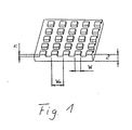
- the depth of the recesses h formed between the protrusions was 0.05 mm in this example and the ratios w: w 0 had a ratio of 1: 2.
- electrostatic holding elements can the respective size of the contact surfaces optimized for the respective application.
- One additional parameters, in particular for the respectively achievable Electrostatic holding forces is as well the depth of recesses h over which the respective Shares in the holding forces that cross the Coulombund the Johnson-Rahbek behavior will be applied can, are influenceable and above that too which particle size is deposited there can be before a deformation of the overlying Substrate or element takes place.
- the Figures 1 and 2 shown examples was produced according to Ensures that all touch surfaces with a tolerance ⁇ 1 ⁇ m within a common Level lay and so a plateau surface for an element or substrate on a surface of at least 150 mm ⁇ 150 mm or over a diameter of 200 mm.
Landscapes
- Physics & Mathematics (AREA)
- General Physics & Mathematics (AREA)
- Container, Conveyance, Adherence, Positioning, Of Wafer (AREA)
Abstract
Description
- Figur 1
- eine perspektivische Darstellung eines Beispiels eines erfindungsgemäßen elektrostatischen Halteelementes mit einer Oberflächenstrukturierung in Form von quaderförmigen Erhöhungen und
- Figur 2
- eine perspektivische Darstellung eines Beispiels für ein elektrostatisches Halteelement mit einer Strukturierung in Form zylinderförmiger Erhebungen.
Claims (18)
- Elektrostatisches Halteelement für bei der lithographischen Strukturierung von Halbleiterelementen zu fixierenden Elementen oder Substraten für Halbleiterelemente, das aus einem Werkstoff, der einen spezifischen elektrischen Widerstand bei einer Temperatur von 20 °C > 1013 Ωcm
und einen Wärmeausdehnungskoeffizienten, dessen absoluter Betrag mindestens im Temperaturbereich zwischen 0 und 50 °C < 10-7/K aufweist,
besteht sowie der dielektrische Teil des Halteelementes eine Dicke < 0,5 mm aufweist und die Oberfläche zum Halten des Elementes oder Substrates strukturiert ist. - Halteelement nach Anspruch 1,
dadurch gekennzeichnet, dass der Werkstoff ein Alkali/Erdalkali - Alumino - Silikat in einer SiO2-Matrix ist. - Halteelement nach Anspruch 1 oder 2,
dadurch gekennzeichnet, dass das Alkali/Erdalkali - Alumino - Silikat LiAlSiO4, LiAl-Si2O6 oder Zn0,5AlSi2O6 ist. - Halteelement nach mindestens einem der vorhergehenden Ansprüche, dadurch gekennzeichnet, dass die Strukturierung in Form von Erhebungen, deren abgeflachte Berührungsflächen in einer gemeinsamen Ebene angeordnet sind, ausgebildet ist, deren Lageabweichungen in Bezug zu dieser Ebene < 1 µm sind.
- Halteelement nach Anspruch 4,
dadurch gekennzeichnet, dass die Erhebungen zylinderförmig, quaderförmig, in Form von Kegeloder Pyramidenstümpfen ausgebildet sind. - Halteelement nach Anspruch 4 oder 5,
dadurch gekennzeichnet, dass zwischen den Erhebungen Vertiefungen ausgebildet sind, deren Tiefe < 0,5 mm und > 0,001 mm ist. - Halteelement nach mindestens einem der Ansprüche 1 bis 5, dadurch gekennzeichnet, dass die Strukturierung in Form von Vertiefungen oder Durchbrechungen ausgebildet ist.
- Halteelement nach mindestens einem der vorhergehenden Ansprüche, dadurch gekennzeichnet, dass die Berührungsflächen für das Element oder Substrat eine mittlere Rauhtiefe Ra und/oder einem quadratischen Mittenrauhwert Rq < 1 µm aufweisen.
- Halteelement nach mindestens einem der vorhergehenden Ansprüche, dadurch gekennzeichnet, dass die Strukturierung über die Fläche des Halteelementes gleichmäßig ausgebildet ist.
- Halteelement nach mindestens einem der vorhergehenden Ansprüche, dadurch gekennzeichnet, dass die Erhebungen, Vertiefungen oder Durchbrechungen jeweils gleich dimensioniert und äquidistant angeordnet sind.
- Halteelement nach mindestens einem der vorhergehenden Ansprüche, dadurch gekennzeichnet, dass das Verhältnis der Summe der Berührungsflächen in Bezug zur Gesamtfläche des Halteelementes zwischen 1 : 1,01 und 1 : 200 liegt.
- Halteelement nach mindestens einem der vorhergehenden Ansprüche, dadurch gekennzeichnet, dass die Summe der Berührungsflächen innerhalb eines äußeren Randbereiches des Halteelementes mindestens zweimal so groß, wie in einem zentralen Innenbereich des Halteelementes ist.
- Halteelement nach Anspruch 12,
dadurch gekennzeichnet, dass die Breite des äußeren Randbereiches ≤ einem viertel der Diagonalen oder des Durchmessers des Halteelementes ist. - Halteelement nach mindestens einem der vorhergehenden Ansprüche, dadurch gekennzeichnet, dass innerhalb eines zentralen Innenbereiches des Halteelementes mindestens eine Durchbrechung ausgebildet ist.
- Halteelement nach mindestens einem der vorhergehenden Ansprüche, dadurch gekennzeichnet, dass an mindestens einer Durchbrechung eine einen Unterdruck erzeugende Einheit angeschlossen oder anschließbar ist.
- Halteelement nach mindestens einem der vorhergehenden Ansprüche, dadurch gekennzeichnet, dass mindestens zwei orthogonal zueinander und orthogonal in Bezug zur Ebene der Berührungsfläche(n) ausgerichtete reflektierende Flächen für eine interferometrische Positonsbestimmung des Halteelementes am Halteelement vorhanden sind.
- Halteelement nach Anspruch 16,
dadurch gekennzeichnet, dass die mittlere Rauhtiefe Ra und/oder der quadratische Mittenrauhwert Rq der reflektierenden Flächen < 0,05 µm ist. - Halteelement nach mindestens einem der vorhergehenden Ansprüche, dadurch gekennzeichnet, dass das mit dem Halteelement zu fixierende Element oder Substrat eine Maske oder ein Wafer ist.
Applications Claiming Priority (4)
| Application Number | Priority Date | Filing Date | Title |
|---|---|---|---|
| DE10230660 | 2002-07-01 | ||
| DE10230660 | 2002-07-01 | ||
| DE10240356A DE10240356B4 (de) | 2002-07-01 | 2002-08-27 | Elektrostatisches Halteelement |
| DE10240356 | 2002-08-27 |
Publications (3)
| Publication Number | Publication Date |
|---|---|
| EP1378936A2 true EP1378936A2 (de) | 2004-01-07 |
| EP1378936A3 EP1378936A3 (de) | 2005-01-26 |
| EP1378936B1 EP1378936B1 (de) | 2011-01-19 |
Family
ID=29720540
Family Applications (1)
| Application Number | Title | Priority Date | Filing Date |
|---|---|---|---|
| EP03013693A Expired - Lifetime EP1378936B1 (de) | 2002-07-01 | 2003-06-17 | Elektrostatisches Halteelement |
Country Status (1)
| Country | Link |
|---|---|
| EP (1) | EP1378936B1 (de) |
Cited By (4)
| Publication number | Priority date | Publication date | Assignee | Title |
|---|---|---|---|---|
| EP1510868A1 (de) * | 2003-08-29 | 2005-03-02 | ASML Netherlands B.V. | Lithographischer Apparat und Verfahren zur Herstellung eines Artikels |
| WO2005036637A1 (en) * | 2003-10-10 | 2005-04-21 | Axcelis Technologies Inc. | Mems based contact conductivity electrostatic chuck |
| US7110091B2 (en) | 2003-07-23 | 2006-09-19 | Asml Netherlands B.V. | Lithographic apparatus, device manufacturing method, and device manufactured thereby |
| EP1500984A3 (de) * | 2003-07-23 | 2009-06-17 | ASML Netherlands B.V. | Lithographischer Apparat, Verfahren zur Herstellung eines Artikels und dabei hergestellter Artikel |
Citations (1)
| Publication number | Priority date | Publication date | Assignee | Title |
|---|---|---|---|---|
| US5777838A (en) | 1995-12-19 | 1998-07-07 | Fujitsu Limited | Electrostatic chuck and method of attracting wafer |
Family Cites Families (2)
| Publication number | Priority date | Publication date | Assignee | Title |
|---|---|---|---|---|
| US5886863A (en) * | 1995-05-09 | 1999-03-23 | Kyocera Corporation | Wafer support member |
| JP2000323558A (ja) * | 1999-05-07 | 2000-11-24 | Nikon Corp | 静電吸着装置 |
-
2003
- 2003-06-17 EP EP03013693A patent/EP1378936B1/de not_active Expired - Lifetime
Patent Citations (1)
| Publication number | Priority date | Publication date | Assignee | Title |
|---|---|---|---|---|
| US5777838A (en) | 1995-12-19 | 1998-07-07 | Fujitsu Limited | Electrostatic chuck and method of attracting wafer |
Cited By (6)
| Publication number | Priority date | Publication date | Assignee | Title |
|---|---|---|---|---|
| US7110091B2 (en) | 2003-07-23 | 2006-09-19 | Asml Netherlands B.V. | Lithographic apparatus, device manufacturing method, and device manufactured thereby |
| US7528935B2 (en) | 2003-07-23 | 2009-05-05 | Asml Netherlands B.V. | Lithographic apparatus, device manufacturing method, and device manufactured thereby |
| EP1500984A3 (de) * | 2003-07-23 | 2009-06-17 | ASML Netherlands B.V. | Lithographischer Apparat, Verfahren zur Herstellung eines Artikels und dabei hergestellter Artikel |
| EP1510868A1 (de) * | 2003-08-29 | 2005-03-02 | ASML Netherlands B.V. | Lithographischer Apparat und Verfahren zur Herstellung eines Artikels |
| US7119885B2 (en) | 2003-08-29 | 2006-10-10 | Asml Netherlands B.V. | Lithographic apparatus and device manufacturing method |
| WO2005036637A1 (en) * | 2003-10-10 | 2005-04-21 | Axcelis Technologies Inc. | Mems based contact conductivity electrostatic chuck |
Also Published As
| Publication number | Publication date |
|---|---|
| EP1378936B1 (de) | 2011-01-19 |
| EP1378936A3 (de) | 2005-01-26 |
Similar Documents
| Publication | Publication Date | Title |
|---|---|---|
| DE69937591T2 (de) | Selektive Verlegung von Elementen von einem Träger zu einem anderen Träger | |
| DE10138882B4 (de) | Großflächige Membranmaske und Verfahren zu ihrer Herstellung | |
| DE68910368T2 (de) | Verfahren zum Herstellen eines Halbleiterkörpers. | |
| DE4434321C2 (de) | Optischer Wellenleiter mit einem Polymerkern und dessen Herstellungsverfahren | |
| DE102014200869B4 (de) | Integrierter Kondensator und Verfahren zum Herstellen desselben und dessen Verwendung | |
| DE102005040267B4 (de) | Verfahren zum Herstellen einer mehrschichtigen elektrostatischen Linsenanordnung, insbesondere einer Phasenplatte und derartige Phasenplatte | |
| EP0019779A2 (de) | Schattenwurfmaske zum Strukturieren von Oberflächenbereichen und Verfahren zu ihrer Herstellung | |
| DE69025831T2 (de) | Elektronemittierende Vorrichtung; Herstellungsverfahren Elektronemittierende Vorrichtung, Herstellungsverfahren derselben und Anzeigegerät und Elektronstrahl- Schreibvorrichtung, welche diese Vorrichtung verwendet. | |
| WO2003088340A2 (de) | Verfahren zur herstellung strukturierter schichten auf substraten | |
| DE10030352A1 (de) | Mikromechanisches Bauelement, insbesondere Sensorelement, mit einer stabilisierten Membran und Verfahren zur Herstellung eines derartigen Bauelements | |
| EP1371092A1 (de) | Verfahren zur strukturierung eines aus glasartigen material bestehenden flächensubstrats | |
| DE19708766C2 (de) | Lithographiemaske und Verfahren zur Herstellung derselben | |
| DE69730143T2 (de) | Feldemissionselektronenquelle und sein Herstellungsverfahren | |
| DE19710798C1 (de) | Herstellverfahren für Membranmaske mit Maskenfeldern | |
| EP1378936B1 (de) | Elektrostatisches Halteelement | |
| DE102013109143A1 (de) | Photozelle, insbesondere Solarzelle sowie Verfahren zum Herstellen einer Photozelle | |
| DE10240356B4 (de) | Elektrostatisches Halteelement | |
| EP0835474B1 (de) | Mikromechanische Bewegungseinrichtung zur Ablenkung von Lichtstrahlen und Verfahren zu deren Herstellung | |
| DE102019127649A1 (de) | Halbleiterbauelement und Anordnung zur Kontaktierung des Halbleiterbauelements beim anodischen Bonden eines Glassubstrats mit Kontaktdurchführungen an ein Siliziumsubstrat | |
| DE60224808T2 (de) | Hintere feldemissionsplatte | |
| WO2003008323A2 (de) | Hebe- und stützvorrichtung | |
| DE4209301C1 (en) | Manufacture of controlled field emitter for flat display screen, TV etc. - using successive etching and deposition stages to form cone shaped emitter peak set in insulating matrix together with electrodes | |
| DE102007010462B4 (de) | Verfahren zur Herstellung einer Teilchenstrahlquelle | |
| EP1289876B1 (de) | Mikrostruktur und verfahren zu deren herstellung | |
| DE102004058103B4 (de) | Einrichtung zur Spalteinstellung |
Legal Events
| Date | Code | Title | Description |
|---|---|---|---|
| PUAI | Public reference made under article 153(3) epc to a published international application that has entered the european phase |
Free format text: ORIGINAL CODE: 0009012 |
|
| AK | Designated contracting states |
Kind code of ref document: A2 Designated state(s): AT BE BG CH CY CZ DE DK EE ES FI FR GB GR HU IE IT LI LU MC NL PT RO SE SI SK TR |
|
| AX | Request for extension of the european patent |
Extension state: AL LT LV MK |
|
| PUAL | Search report despatched |
Free format text: ORIGINAL CODE: 0009013 |
|
| AK | Designated contracting states |
Kind code of ref document: A3 Designated state(s): AT BE BG CH CY CZ DE DK EE ES FI FR GB GR HU IE IT LI LU MC NL PT RO SE SI SK TR |
|
| AX | Request for extension of the european patent |
Extension state: AL LT LV MK |
|
| 17P | Request for examination filed |
Effective date: 20050315 |
|
| AKX | Designation fees paid |
Designated state(s): AT BE BG CH CY CZ DE DK EE ES FI FR GB GR HU IE IT LI LU MC NL PT RO SE SI SK TR |
|
| RAP1 | Party data changed (applicant data changed or rights of an application transferred) |
Owner name: FRAUNHOFER-GESELLSCHAFT ZUR FOERDERUNG DER ANGEWAN |
|
| GRAP | Despatch of communication of intention to grant a patent |
Free format text: ORIGINAL CODE: EPIDOSNIGR1 |
|
| GRAS | Grant fee paid |
Free format text: ORIGINAL CODE: EPIDOSNIGR3 |
|
| GRAA | (expected) grant |
Free format text: ORIGINAL CODE: 0009210 |
|
| AK | Designated contracting states |
Kind code of ref document: B1 Designated state(s): AT BE BG CH CY CZ DE DK EE ES FI FR GB GR HU IE IT LI LU MC NL PT RO SE SI SK TR |
|
| REG | Reference to a national code |
Ref country code: GB Ref legal event code: FG4D Free format text: NOT ENGLISH |
|
| REG | Reference to a national code |
Ref country code: CH Ref legal event code: EP |
|
| REG | Reference to a national code |
Ref country code: IE Ref legal event code: FG4D Free format text: LANGUAGE OF EP DOCUMENT: GERMAN |
|
| REF | Corresponds to: |
Ref document number: 50313419 Country of ref document: DE Date of ref document: 20110303 Kind code of ref document: P |
|
| REG | Reference to a national code |
Ref country code: DE Ref legal event code: R096 Ref document number: 50313419 Country of ref document: DE Effective date: 20110303 |
|
| REG | Reference to a national code |
Ref country code: NL Ref legal event code: T3 |
|
| PG25 | Lapsed in a contracting state [announced via postgrant information from national office to epo] |
Ref country code: PT Free format text: LAPSE BECAUSE OF FAILURE TO SUBMIT A TRANSLATION OF THE DESCRIPTION OR TO PAY THE FEE WITHIN THE PRESCRIBED TIME-LIMIT Effective date: 20110519 Ref country code: GR Free format text: LAPSE BECAUSE OF FAILURE TO SUBMIT A TRANSLATION OF THE DESCRIPTION OR TO PAY THE FEE WITHIN THE PRESCRIBED TIME-LIMIT Effective date: 20110420 Ref country code: SE Free format text: LAPSE BECAUSE OF FAILURE TO SUBMIT A TRANSLATION OF THE DESCRIPTION OR TO PAY THE FEE WITHIN THE PRESCRIBED TIME-LIMIT Effective date: 20110119 Ref country code: ES Free format text: LAPSE BECAUSE OF FAILURE TO SUBMIT A TRANSLATION OF THE DESCRIPTION OR TO PAY THE FEE WITHIN THE PRESCRIBED TIME-LIMIT Effective date: 20110430 |
|
| REG | Reference to a national code |
Ref country code: IE Ref legal event code: FD4D |
|
| PG25 | Lapsed in a contracting state [announced via postgrant information from national office to epo] |
Ref country code: BG Free format text: LAPSE BECAUSE OF FAILURE TO SUBMIT A TRANSLATION OF THE DESCRIPTION OR TO PAY THE FEE WITHIN THE PRESCRIBED TIME-LIMIT Effective date: 20110419 Ref country code: CY Free format text: LAPSE BECAUSE OF FAILURE TO SUBMIT A TRANSLATION OF THE DESCRIPTION OR TO PAY THE FEE WITHIN THE PRESCRIBED TIME-LIMIT Effective date: 20110119 Ref country code: SI Free format text: LAPSE BECAUSE OF FAILURE TO SUBMIT A TRANSLATION OF THE DESCRIPTION OR TO PAY THE FEE WITHIN THE PRESCRIBED TIME-LIMIT Effective date: 20110119 Ref country code: FI Free format text: LAPSE BECAUSE OF FAILURE TO SUBMIT A TRANSLATION OF THE DESCRIPTION OR TO PAY THE FEE WITHIN THE PRESCRIBED TIME-LIMIT Effective date: 20110119 |
|
| PG25 | Lapsed in a contracting state [announced via postgrant information from national office to epo] |
Ref country code: EE Free format text: LAPSE BECAUSE OF FAILURE TO SUBMIT A TRANSLATION OF THE DESCRIPTION OR TO PAY THE FEE WITHIN THE PRESCRIBED TIME-LIMIT Effective date: 20110119 Ref country code: IE Free format text: LAPSE BECAUSE OF FAILURE TO SUBMIT A TRANSLATION OF THE DESCRIPTION OR TO PAY THE FEE WITHIN THE PRESCRIBED TIME-LIMIT Effective date: 20110119 Ref country code: DK Free format text: LAPSE BECAUSE OF FAILURE TO SUBMIT A TRANSLATION OF THE DESCRIPTION OR TO PAY THE FEE WITHIN THE PRESCRIBED TIME-LIMIT Effective date: 20110119 |
|
| PLBE | No opposition filed within time limit |
Free format text: ORIGINAL CODE: 0009261 |
|
| STAA | Information on the status of an ep patent application or granted ep patent |
Free format text: STATUS: NO OPPOSITION FILED WITHIN TIME LIMIT |
|
| PG25 | Lapsed in a contracting state [announced via postgrant information from national office to epo] |
Ref country code: SK Free format text: LAPSE BECAUSE OF FAILURE TO SUBMIT A TRANSLATION OF THE DESCRIPTION OR TO PAY THE FEE WITHIN THE PRESCRIBED TIME-LIMIT Effective date: 20110119 Ref country code: RO Free format text: LAPSE BECAUSE OF FAILURE TO SUBMIT A TRANSLATION OF THE DESCRIPTION OR TO PAY THE FEE WITHIN THE PRESCRIBED TIME-LIMIT Effective date: 20110119 Ref country code: CZ Free format text: LAPSE BECAUSE OF FAILURE TO SUBMIT A TRANSLATION OF THE DESCRIPTION OR TO PAY THE FEE WITHIN THE PRESCRIBED TIME-LIMIT Effective date: 20110119 |
|
| 26N | No opposition filed |
Effective date: 20111020 |
|
| PG25 | Lapsed in a contracting state [announced via postgrant information from national office to epo] |
Ref country code: IT Free format text: LAPSE BECAUSE OF FAILURE TO SUBMIT A TRANSLATION OF THE DESCRIPTION OR TO PAY THE FEE WITHIN THE PRESCRIBED TIME-LIMIT Effective date: 20110119 |
|
| REG | Reference to a national code |
Ref country code: CH Ref legal event code: PL |
|
| REG | Reference to a national code |
Ref country code: DE Ref legal event code: R097 Ref document number: 50313419 Country of ref document: DE Effective date: 20111020 |
|
| PG25 | Lapsed in a contracting state [announced via postgrant information from national office to epo] |
Ref country code: CH Free format text: LAPSE BECAUSE OF NON-PAYMENT OF DUE FEES Effective date: 20110630 Ref country code: LI Free format text: LAPSE BECAUSE OF NON-PAYMENT OF DUE FEES Effective date: 20110630 |
|
| REG | Reference to a national code |
Ref country code: AT Ref legal event code: MM01 Ref document number: 496395 Country of ref document: AT Kind code of ref document: T Effective date: 20110617 |
|
| PG25 | Lapsed in a contracting state [announced via postgrant information from national office to epo] |
Ref country code: AT Free format text: LAPSE BECAUSE OF NON-PAYMENT OF DUE FEES Effective date: 20110617 |
|
| PG25 | Lapsed in a contracting state [announced via postgrant information from national office to epo] |
Ref country code: MC Free format text: LAPSE BECAUSE OF NON-PAYMENT OF DUE FEES Effective date: 20110630 |
|
| PG25 | Lapsed in a contracting state [announced via postgrant information from national office to epo] |
Ref country code: LU Free format text: LAPSE BECAUSE OF NON-PAYMENT OF DUE FEES Effective date: 20110617 |
|
| PG25 | Lapsed in a contracting state [announced via postgrant information from national office to epo] |
Ref country code: TR Free format text: LAPSE BECAUSE OF FAILURE TO SUBMIT A TRANSLATION OF THE DESCRIPTION OR TO PAY THE FEE WITHIN THE PRESCRIBED TIME-LIMIT Effective date: 20110119 |
|
| PG25 | Lapsed in a contracting state [announced via postgrant information from national office to epo] |
Ref country code: HU Free format text: LAPSE BECAUSE OF FAILURE TO SUBMIT A TRANSLATION OF THE DESCRIPTION OR TO PAY THE FEE WITHIN THE PRESCRIBED TIME-LIMIT Effective date: 20110119 |
|
| REG | Reference to a national code |
Ref country code: FR Ref legal event code: PLFP Year of fee payment: 13 |
|
| PGFP | Annual fee paid to national office [announced via postgrant information from national office to epo] |
Ref country code: GB Payment date: 20150623 Year of fee payment: 13 |
|
| PGFP | Annual fee paid to national office [announced via postgrant information from national office to epo] |
Ref country code: FR Payment date: 20150623 Year of fee payment: 13 Ref country code: BE Payment date: 20150617 Year of fee payment: 13 |
|
| PG25 | Lapsed in a contracting state [announced via postgrant information from national office to epo] |
Ref country code: BE Free format text: LAPSE BECAUSE OF NON-PAYMENT OF DUE FEES Effective date: 20160630 |
|
| GBPC | Gb: european patent ceased through non-payment of renewal fee |
Effective date: 20160617 |
|
| REG | Reference to a national code |
Ref country code: FR Ref legal event code: ST Effective date: 20170228 |
|
| PG25 | Lapsed in a contracting state [announced via postgrant information from national office to epo] |
Ref country code: FR Free format text: LAPSE BECAUSE OF NON-PAYMENT OF DUE FEES Effective date: 20160630 |
|
| PG25 | Lapsed in a contracting state [announced via postgrant information from national office to epo] |
Ref country code: GB Free format text: LAPSE BECAUSE OF NON-PAYMENT OF DUE FEES Effective date: 20160617 |
|
| PGFP | Annual fee paid to national office [announced via postgrant information from national office to epo] |
Ref country code: DE Payment date: 20200623 Year of fee payment: 18 |
|
| PGFP | Annual fee paid to national office [announced via postgrant information from national office to epo] |
Ref country code: NL Payment date: 20200622 Year of fee payment: 18 |
|
| REG | Reference to a national code |
Ref country code: DE Ref legal event code: R119 Ref document number: 50313419 Country of ref document: DE |
|
| REG | Reference to a national code |
Ref country code: NL Ref legal event code: MM Effective date: 20210701 |
|
| PG25 | Lapsed in a contracting state [announced via postgrant information from national office to epo] |
Ref country code: DE Free format text: LAPSE BECAUSE OF NON-PAYMENT OF DUE FEES Effective date: 20220101 |
|
| PG25 | Lapsed in a contracting state [announced via postgrant information from national office to epo] |
Ref country code: NL Free format text: LAPSE BECAUSE OF NON-PAYMENT OF DUE FEES Effective date: 20210701 |