EP1376751A1 - Connection structure of connector pin and signal line and semiconductor package using it - Google Patents
Connection structure of connector pin and signal line and semiconductor package using it Download PDFInfo
- Publication number
- EP1376751A1 EP1376751A1 EP02715791A EP02715791A EP1376751A1 EP 1376751 A1 EP1376751 A1 EP 1376751A1 EP 02715791 A EP02715791 A EP 02715791A EP 02715791 A EP02715791 A EP 02715791A EP 1376751 A1 EP1376751 A1 EP 1376751A1
- Authority
- EP
- European Patent Office
- Prior art keywords
- signal line
- connector pin
- width
- signal
- connection structure
- Prior art date
- Legal status (The legal status is an assumption and is not a legal conclusion. Google has not performed a legal analysis and makes no representation as to the accuracy of the status listed.)
- Withdrawn
Links
Images



Classifications
-
- H—ELECTRICITY
- H01—ELECTRIC ELEMENTS
- H01P—WAVEGUIDES; RESONATORS, LINES, OR OTHER DEVICES OF THE WAVEGUIDE TYPE
- H01P5/00—Coupling devices of the waveguide type
- H01P5/08—Coupling devices of the waveguide type for linking dissimilar lines or devices
- H01P5/085—Coaxial-line/strip-line transitions
Definitions
- This invention relates to a structure of a semiconductor package for a high frequency device; and particularly to a connection structure of a circuit board provided with a signal line of a planer waveguide and a connector pin.
- the present invention is applicable to both a microstrip line and a coplanar line.
- Figure 15 is a fragmentary sectional view of the connection structure of a connector pin 103 and a signal line 106 in a semiconductor package 100.
- 101 is a part of the package frame.
- a glass bead 102 connected to the termination of the coaxial line proceeds in the arrow X direction and is guided in a blind hole 104 set up in the package frame 101.
- a recessed groove 107 into which connector pin 103 is inserted is formed at the junction of an end of the signal line 106 formed on a dielectric substrate 105.
- connection structure proposed in Japanese Patent Laying-Open No. 11-224757 lacks sufficiency to minimize a transmission loss in the high frequency area of the signal, especially when the frequency of the signal becomes high and a connector pin diameter becomes small: In other words, when the connector pin diameter becomes small, positioning of the recessed groove and the connector pin becomes difficult. In addition; there is the concern for the occurrence of transmission loss to the signal line, which is a planer waveguide, due to a change in the position of the top and bottom of the signal line and the connector pin, and the occurrence of transmission loss due to discontinuity of circuit width caused by a variation in the coating amount of the solder filled in the recessed groove.
- An object of the present invention is to minimize the above-described factors that cause the transmission loss of the signal at the high frequency area and to restrain radiation and reflection.
- connection structure of a signal line and a connector pin in a semiconductor package is such that the width of the signal line connected to the connector pin is made narrower than the width of a signal line which can match the connector characteristic impedance.
- the junction with the above connection structure is a junction for leading an electrical signal transmitted through a coaxial line to a thin film signal line, which is a planer waveguide formed on a dielectric substrate, from the tip of a connector pin piercing through an insulating glass bead.
- the junction part is a junction that transmits an electrical signal, which is converted from an optical signal transmitted through an optical fiber by an optical semiconductor device, to a coaxial line.
- the width of the signal line is made narrower at the junction part that is connected with the connector pin than the projection width of a connector pin diameter.
- the width of the signal line is increased gradually from the narrow width of the junction part connected with the connector pin to the wide width of a non-junction part of the signal line.
- Figure 1 shows a schematic perspective view of a semiconductor package which has a connection structure of a connector pin and a signal line of the present invention.
- a high frequency signal transmitted through a coaxial line (not illustrated in the figure) is transmitted to a connector pin 1 which pierces through the inside of an insulating glass bead 2.
- the periphery of the glass bead 2 is pushed into a hole of a package frame 9 consisting of Cu-W alloys or Fe-Ni alloys and it is fixed.
- a loading base 10 made of the same metal as the package frame 9 is bonded to a bottom part of the semiconductor package with the brazing filler metal.
- a thin film signal line 3 is formed, by vacuum evaporation or plating of low resistance metal such as gold, on a dielectric substrate 4 which consists of aluminum nitride and so on.
- the connector pin 1 and the signal line are connected together with solder 5.
- An insulating substrate of high heat radiation (not illustrated in the figure) is installed inside the semiconductor package.
- An optical semiconductor device such as a laser diode for changing an electrical signal to an optical signal or a photo diode for changing an optical signal to an electrical signal, a Peltier element that is an electronic cooling element, a capacitor, a resistance, and so on are mounted on package. These elements are connected with the signal line 3 or the metallized lines 8 by wire bonding and so on, and these elements are driven by the electric power supplied from the lead frame 7, and they are made to work as a semiconductor module.
- a window 11 is used for input and output of the optical signal between an optical fiber and the module.
- Figure 2 is an enlarged plan view of the signal line 3 around the part A in Fig. 1.
- the signal line 3 made of the thin film deposited on the dielectric substrate 4 by vacuum evaporation has a width of B 1 at the non-junction part, and the width B 2 at a junction part 3a connected with the connector pin 1 is set smaller than the non junction part. It is desirable that the width B 2 of the junction part 3a is 0.4 ⁇ 0.7, assuming the width B 1 of the non-junction part of the signal line 3 to bel.
- the width is increased gradually from the width B 2 to the width B 1 .
- the change from the width B 2 to the width B 1 is at an optional angle ⁇ inclining toward the non-junction part Such that the following relation (1) is satisfied, where ⁇ is an inclination angle and S is the width of a transition part.
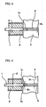
- Figure 3 illustrates an outline 1a of a connector pin 1 as projected on a signal line 3 in a plan view of the part A of Fig. 1.
- the actual size of the width B 1 of the signal line 3 in Comparative Example 1 is formed in the uniform size of 0.23 mm as illustrated, and the relative dielectric constant of the circuit board is 9.0.
- a pin diameter a of the connector pin 1 penetrating through a glass bead 2 is 0.23 mm, and the relative dielectric constant of the glass is 4.4.
- the connector pin 1 and the signal line 3 were connected with a predetermined quantity of solder.
- Figure 4 illustrates an outline 1a of a connector pin 1 as projected on a signal line 3 in a plan view of the part A of Fig. 1.
- the actual size of the width B 1 of the signal line 3 on a dielectric substrate is 0.23mm
- the width B 2 of the signal line 3a in a junction part is 0.12mm, as illustrated, in Example 1.
- the change of the width from the signal line 3a of the junction part to the signal line 3 of the non-junction part was made through a right angle corner.
- the pin diameter d of a connector pin 1 penetrating through a glass bead 2 was 0.23 mm, the same as in Comparative Example 1.
- the quantity of solder for connecting the connector pin 1 and the signal line 3 was set equal to that of Comparative Example 1.
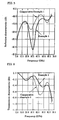
- Figure 5 is a semilogarithm graph showing the frequency dependence of the reflection and it indicates that the reflection is smaller as the minus number is smaller (that is, the absolute value is larger).
- the horizontal axis represents frequency and the vertical axis represents reflection characteristic
- the thin line is the simulation calculation result showing the reflection characteristic in Comparative Example 1 illustrated in Fig. 3.
- the thick line in Fig. 5 is a simulation calculation result of the reflection characteristic of Example 1 in Fig. 4.
- the reflection characteristic of Example 1 is better than that of Comparative Example 1 remarkably in the high frequency range from the frequency exceeding about 20GHz to the frequency slightly exceeding 50GHz.
- Figure 6 a graph plotting an evaluation result of the transmission characteristic of the signal and shows that the signal is transmitted without loss of the signal as a plot approaches zero in the ordinate.
- the thin line is a simulation calculation result showing the transmission characteristic of Comparative Example in Fig. 3.
- the thick line is a simulation calculation result of the transmission characteristic of Example 1 in Fig. 4.
- the transmission characteristic of Example 1 is better than that of Comparative Example 1 in the high frequency range from the frequency of about 30GHz to the frequency of slightly exceeding 50GHz.
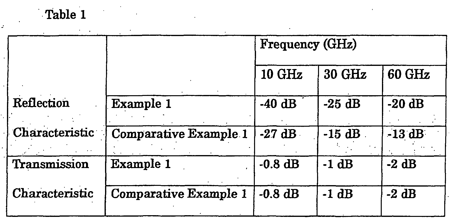
- Example 1 The samples of the same specifications as those of Example 1 and Comparative Example 1 were prepared, and the results of measuring their reflection and transmission characteristics by a network analyzer are shown in Table 1 for reference to prove the reliability of the simulation calculation results.
- Example 1 was better than Comparative Example 1 in the wide frequency range.
- Comparative Example 1 shown in Fig. 3 and Comparative Example 2 shown in Fig. 7 are evaluated.
- the calculation model of a connection structure of Comparative Example 2 of Fig. 7 is basically the same as Comparative Example 1 in which the center of the connector pin 1 coincides with the center of the signal line 3, except that deviation of the border line 1a of the connector pin 1 and the outside of the signal line 3 is 0.1 mm.
- the broken line is the result of a simulation calculation showing the reflection characteristics of Comparative Example 2 of Fig. 7, and the solid line is the reflection characteristic of Comparative Example 1.
- Example 2 that was prepared for comparison with Example 1 is shown in Fig. 10.
- the calculation model of a connection structure of Example 2 is basically the same as Example 1 in which the center of the connector pin 1 coincides with the center of the signal line 3, except that deviation of the border line 1a of the connector pin 1 arid the outside of the signal line 3 is 0.1 mm.
- the dotted line is the result of a simulation calculation which shows the reflection characteristics of Example 2 of Fig. 10
- the solid line is the reflection characteristics of Example 1.
- Example 1 has slightly better reflection characteristic than Example 2 at the frequency around 30 GHz.
- Example 1 has better transmission characteristic than Example 2 in the frequency range from about 30 GHz to 60 GHz, but the difference between Example 1 and Example 2 is slight. It is proved that the connection structure of Example 2 receives less influence of the deviation on both characteristics than Comparative Example 2 which has the same deviation as Example 2. Therefore, it is possible to conclude that Examples of the present invention are minimally affected by the assembling error.
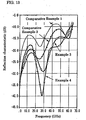
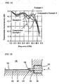
- Comparative Example 1 is shown by a thin line and Comparative Example 3 is shown by a thick line with filled circles, Example 3 is shown by a thick line with open circles and Example 4 is shown by a thick line with open triangles.
- Examples 3 and 4 show good results in the high frequency range from the frequency exceeding about 20 GHz to 55 GHz.
- the reflection of Comparative Example 1 is large and Comparative Example 3 also shows the tendency of the large reflection.
- Comparative Example 3 has a partial frequency range of a good transmission characteristic, however, it is limited to the small frequency range. It is considered that the joint structure having excellent reflection and transmission characteristics in the high frequency range of 20 - 55 GHz can be obtained by setting the line width ratio B 2 /B 1 of the junction part of the signal line to 0.4- 0.7.
- connection structure of a connector pin and a signal line In the connection structure of a connector pin and a signal line, the radiation and the reflection of the signal in a junction part is minimized and the deterioration of the transmission loss can be prevented by a structure in which the width of a signal line connected with a connector pin is made narrower than the width of a signal line which can coincide with the connector characteristic impedance, and the width of the junction part of the signal line is made narrower than the projection width of the connector pin diameter. Moreover, the assembling error of the connector pin and the signal line is absorbed in the semiconductor package having such connection structure and the deterioration of the transmission loss of the signal can be prevented.
Landscapes
- Coupling Device And Connection With Printed Circuit (AREA)
- Semiconductor Lasers (AREA)
Abstract
The width of a signal line 3 is made narrower at a part connected with a connector
pin 1 than a signal line width that can match the connector characteristic
impedance. Furthermore, the width of the signal line 3 is made narrower at
the part connected with the connector pin 1 than the projection width of the
connector pin diameter. The disclosed connection structure of a planer
waveguide signal line can, when a high frequency signal is transmitted from a
rod-shaped coaxial structure to the signal line, prevent the transmissivity deterioration
caused by radiation of the signal or reflection of the signal back to the
outgoing side at the part of the signal line connected with a connector pin. The
connection structure can also minimize transmission loss due to assembling
error made during assembling into a semiconductor package.
Description
This invention relates to a structure of a semiconductor package for a high
frequency device; and particularly to a connection structure of a circuit board
provided with a signal line of a planer waveguide and a connector pin.
Recently, a semiconductor package for high frequency having a signal line
circuit that efficiently transmits a high frequency signal exceeding several GHz
is demanded, to comply with increased working speed of a semiconductor element
and high frequency to raise signal density.
As for such a semiconductor package for high frequency, it is necessary to
restrain the reflection and loss of the signal at a junction when the high frequency
signal transmitted through a coaxial line is transmitted to the various
semiconductor devices through the connector pin, the junction, and the signal
line of the planer waveguide. The effect of such restraining is especially remarkable
as the signal becomes high frequency. Though there are various
forms of the planer waveguide, the present invention is applicable to both a
microstrip line and a coplanar line.
An example of a structure in which a connector pin and a signal line are connected
with high accuracy is proposed in Japanese Patent Laying-Open No.
11-224757. Figure 15 is a fragmentary sectional view of the connection structure
of a connector pin 103 and a signal line 106 in a semiconductor package
100. In Fig. 15, 101 is a part of the package frame. A glass bead 102 connected
to the termination of the coaxial line proceeds in the arrow X direction and is
guided in a blind hole 104 set up in the package frame 101. On the other hand,
a recessed groove 107 into which connector pin 103 is inserted is formed at the
junction of an end of the signal line 106 formed on a dielectric substrate 105.
When the connector pin 103 and the signal line 106 are connected, both are
made to fit so that a recessed groove 107 may hold the tip of the connector pin
103, and they are finally connected by a solder 108. It is explained that the
connector pin 103 and the recessed groove 107 are positioned properly by such
a structure, and the positioning accuracy of the connector pin 103 and the signal
line 106 improves automatically. But if the position of the end of the connector
pin 103 and the position of the recessed groove 107 formed on the dielectric
substrate 105 are not accurate, they cannot be connected physically.
The connection structure proposed in Japanese Patent Laying-Open No. 11-224757
lacks sufficiency to minimize a transmission loss in the high frequency
area of the signal, especially when the frequency of the signal becomes high
and a connector pin diameter becomes small: In other words, when the connector
pin diameter becomes small, positioning of the recessed groove and the connector
pin becomes difficult. In addition; there is the concern for the occurrence
of transmission loss to the signal line, which is a planer waveguide, due to a
change in the position of the top and bottom of the signal line and the connector
pin, and the occurrence of transmission loss due to discontinuity of circuit
width caused by a variation in the coating amount of the solder filled in the
recessed groove.
An object of the present invention is to minimize the above-described factors
that cause the transmission loss of the signal at the high frequency area and to
restrain radiation and reflection.
The connection structure of a signal line and a connector pin in a semiconductor
package according to an embodiment of the present invention is such
that the width of the signal line connected to the connector pin is made narrower
than the width of a signal line which can match the connector characteristic
impedance.
The junction with the above connection structure is a junction for leading an
electrical signal transmitted through a coaxial line to a thin film signal line,
which is a planer waveguide formed on a dielectric substrate, from the tip of a
connector pin piercing through an insulating glass bead.
Also, the junction part is a junction that transmits an electrical signal, which
is converted from an optical signal transmitted through an optical fiber by an
optical semiconductor device, to a coaxial line.
The width of the signal line is made narrower at the junction part that is
connected with the connector pin than the projection width of a connector pin
diameter.
The width of the signal line is increased gradually from the narrow width of
the junction part connected with the connector pin to the wide width of a non-junction
part of the signal line.
In the drawings:
Examples embodying the present invention are explained in detail with reference
to drawings as follows. Figure 1 shows a schematic perspective view of a
semiconductor package which has a connection structure of a connector pin and
a signal line of the present invention.
A high frequency signal transmitted through a coaxial line (not illustrated in
the figure) is transmitted to a connector pin 1 which pierces through the inside
of an insulating glass bead 2. The periphery of the glass bead 2 is pushed into a
hole of a package frame 9 consisting of Cu-W alloys or Fe-Ni alloys and it is
fixed. A loading base 10 made of the same metal as the package frame 9 is
bonded to a bottom part of the semiconductor package with the brazing filler
metal. A thin film signal line 3 is formed, by vacuum evaporation or plating of
low resistance metal such as gold, on a dielectric substrate 4 which consists of
aluminum nitride and so on. The connector pin 1 and the signal line are connected
together with solder 5.
A ceramic feed through 6, which is attached to an upper part of each side of
the package frame 9, is provided with lead frame 7 that are connected with
metallized lines 8. An insulating substrate of high heat radiation (not illustrated
in the figure) is installed inside the semiconductor package. An optical semiconductor
device such as a laser diode for changing an electrical signal to an
optical signal or a photo diode for changing an optical signal to an electrical
signal, a Peltier element that is an electronic cooling element, a capacitor, a
resistance, and so on are mounted on package. These elements are connected
with the signal line 3 or the metallized lines 8 by wire bonding and so on, and
these elements are driven by the electric power supplied from the lead frame 7,
and they are made to work as a semiconductor module. A window 11 is used for
input and output of the optical signal between an optical fiber and the module.
Figure 2 is an enlarged plan view of the signal line 3 around the part A in Fig.
1. The signal line 3 made of the thin film deposited on the dielectric substrate 4
by vacuum evaporation has a width of B1 at the non-junction part, and the
width B2 at a junction part 3a connected with the connector pin 1 is set smaller
than the non junction part. It is desirable that the width B2 of the junction part
3a is 0.4∼0.7, assuming the width B1 of the non-junction part of the signal line
3 to bel.
Also, preferably, the width is increased gradually from the width B2 to the
width B1. In order to prevent transmission loss due to the abrupt change in the
width of the sgnal line 3, it is desirable that the change from the width B2 to
the width B1 is at an optional angle inclining toward the non-junction part
Such that the following relation (1) is satisfied, where is an inclination angle
and S is the width of a transition part.
tan = 2S/(B1 -B2 )
Thus; making the width change from the width B2 to the width B1 gradual,
and not orthogonal, is effective for reducing the signal reflection.
In the following, the effects obtained by the features of the present invention
are described. Figure 3 illustrates an outline 1a of a connector pin 1 as projected
on a signal line 3 in a plan view of the part A of Fig. 1. The actual size of the
width B1 of the signal line 3 in Comparative Example 1 is formed in the uniform
size of 0.23 mm as illustrated, and the relative dielectric constant of the
circuit board is 9.0. A pin diameter a of the connector pin 1 penetrating through
a glass bead 2 is 0.23 mm, and the relative dielectric constant of the glass is 4.4.
The connector pin 1 and the signal line 3 were connected with a predetermined
quantity of solder.
Figure 4 illustrates an outline 1a of a connector pin 1 as projected on a signal
line 3 in a plan view of the part A of Fig. 1. The actual size of the width B1 of the
signal line 3 on a dielectric substrate is 0.23mm, and the width B2 of the signal
line 3a in a junction part is 0.12mm, as illustrated, in Example 1. The change of
the width from the signal line 3a of the junction part to the signal line 3 of the
non-junction part was made through a right angle corner. The pin diameter d of
a connector pin 1 penetrating through a glass bead 2 was 0.23 mm, the same as
in Comparative Example 1. The quantity of solder for connecting the connector
pin 1 and the signal line 3 was set equal to that of Comparative Example 1. A
simulation was carried out with the samples of Comparative Example 1 and
Example 1. In the simulation, reflection characteristic and transmission characteristic
from the coaxial structure on the left to the planer waveguide on the
right shown in Fig. 3 or Fig. 4 were computed with the finite element method
(FEM). The calculation results are shown in Fig. 5 and Fig. 6.
Figure 5 is a semilogarithm graph showing the frequency dependence of the
reflection and it indicates that the reflection is smaller as the minus number is
smaller (that is, the absolute value is larger). In Fig. 5, the horizontal axis represents
frequency and the vertical axis represents reflection characteristic, and
the thin line is the simulation calculation result showing the reflection characteristic
in Comparative Example 1 illustrated in Fig. 3. The thick line in Fig. 5
is a simulation calculation result of the reflection characteristic of Example 1 in
Fig. 4. As can be seen from Fig. 5, the reflection characteristic of Example 1 is
better than that of Comparative Example 1 remarkably in the high frequency
range from the frequency exceeding about 20GHz to the frequency slightly exceeding
50GHz.
Figure 6 a graph plotting an evaluation result of the transmission characteristic
of the signal and shows that the signal is transmitted without loss of
the signal as a plot approaches zero in the ordinate. The thin line is a simulation
calculation result showing the transmission characteristic of Comparative
Example in Fig. 3. And the thick line is a simulation calculation result of the
transmission characteristic of Example 1 in Fig. 4. In consideration of Fig. 6,
the transmission characteristic of Example 1 is better than that of Comparative
Example 1 in the high frequency range from the frequency of about 30GHz
to the frequency of slightly exceeding 50GHz.
The samples of the same specifications as those of Example 1 and Comparative
Example 1 were prepared, and the results of measuring their reflection
and transmission characteristics by a network analyzer are shown in Table 1
for reference to prove the reliability of the simulation calculation results.
The simulation calculation result and the actual values show the tendency of
correspondence qualitatively though differences of absolute values exist.
Moreover, characteristics of Example 1 were better than Comparative Example
1 in the wide frequency range.
Though it is desirable that the center of the connector pin 1 coincide with the
center of the signal line 3, an assembling error cannot be avoided when the
dielectric substrate 4 is connected with the package frame 9. Figures 8, 9, 11
and 12 show simulation calculation results of the influence.
Comparative Example 1 shown in Fig. 3 and Comparative Example 2 shown
in Fig. 7 are evaluated. The calculation model of a connection structure of
Comparative Example 2 of Fig. 7 is basically the same as Comparative Example
1 in which the center of the connector pin 1 coincides with the center of the
signal line 3, except that deviation of the border line 1a of the connector pin 1
and the outside of the signal line 3 is 0.1 mm. In Fig. 8, the broken line is the
result of a simulation calculation showing the reflection characteristics of
Comparative Example 2 of Fig. 7, and the solid line is the reflection characteristic
of Comparative Example 1. In consideration of Fig. 8, which is the result of
the simulation calculation of the reflection characteristics of Comparative Example
1 and Comparative Example 2, the reflection characteristic of Comparative
Example 1 in which the center of the connector pin 1 and the center of the
signal line 3 coincide is better than that of Comparative Example 2 in the high
frequency range from the frequency exceeding about 20 GHz to the frequency
slightly exceeding 60 GHz. Figure 9 shows the simulation calculation results of
the transmission characteristics. In Fig. 9, the broken line is the result of a
simulation calculation of the transmission characteristics in Comparative Example
2 of Fig. 7, and the thin line is the transmission characteristics of Comparative
Example 1. As can be seen from Fig. 9, Comparative Example 1 in
which the center of the connector pin 1 and the center of the signal line 3 coincide
has better transmission characteristics than Comparative Example 2 in
the high frequency range from the frequency exceeding about 20 GHz to the
frequency of about 60GHz.
Furthermore, Example 2 that was prepared for comparison with Example 1
is shown in Fig. 10. The calculation model of a connection structure of Example
2 is basically the same as Example 1 in which the center of the connector pin 1
coincides with the center of the signal line 3, except that deviation of the border
line 1a of the connector pin 1 arid the outside of the signal line 3 is 0.1 mm. In
Fig. 11, the dotted line is the result of a simulation calculation which shows the
reflection characteristics of Example 2 of Fig. 10, and the solid line is the reflection
characteristics of Example 1. In consideration of Fig. 11 which is the result
of the simulation calculation of the reflection characteristics of Example 1 and
Example 2, Example 1 has slightly better reflection characteristic than Example
2 at the frequency around 30 GHz.
In Fig. 12, the dotted line is a result of the simulation calculation of transmission
characteristics in Example 2 of Fig. 10, and the solid line is the transmission
characteristics of Example 1. In consideration of Fig. 12 which is the
result of the simulation calculation of the transmission characteristics of Example
1 and Example 2, Example 1 has better transmission characteristic than
Example 2 in the frequency range from about 30 GHz to 60 GHz, but the difference
between Example 1 and Example 2 is slight. It is proved that the connection
structure of Example 2 receives less influence of the deviation on both
characteristics than Comparative Example 2 which has the same deviation as
Example 2. Therefore, it is possible to conclude that Examples of the present
invention are minimally affected by the assembling error.
Results on the investigation on the appropriate width of the junction part 3a
of the signal line 3 is explained as follows. The samples prepared had a connector
pin diameter d, the width B1 of a signal line 3 of a circuit part and other
specifications that were the same as in Example 1 illustrated in Fig. 4 except
that in Comparative Example 3, the width B2 of a junction part 3a was 0.05 mm,
in Example 3 the width B2 was 0.1 mm corresponding to 0.4 of the width B1,
and in Example 4 the width B2 was 0.16 mm corresponding to 0.7 of the width
B1. Comparative Example 1 illustrated in Fig. 3 was also prepared for comparison.
A reflection characteristic and a transmission characteristic that were obtained
by using the same simulation calculation as mentioned above are shown
in Fig. 13 and Fig. 14, respectively.
In Fig. 13 and Fig. 14, Comparative Example 1 is shown by a thin line and
Comparative Example 3 is shown by a thick line with filled circles, Example 3
is shown by a thick line with open circles and Example 4 is shown by a thick
line with open triangles.
Considering the results of the simulation calculations of the reflection characteristics
in Fig. 13, Examples 3 and 4 show good results in the high frequency
range from the frequency exceeding about 20 GHz to 55 GHz. On the other
hand, the reflection of Comparative Example 1 is large and Comparative Example
3 also shows the tendency of the large reflection.
Considering the results of the simulation calculations of the transmission
characteristics in Fig. 14, Examples 3 and 4 show good results in the high frequency
range from the frequency of around 10 GHz to 60 GHz. On the other
hand, the transmission characteristics of Comparative Example 1 show an
overall deterioration. Comparative Example 3 has a partial frequency range of
a good transmission characteristic, however, it is limited to the small frequency
range. It is considered that the joint structure having excellent reflection and
transmission characteristics in the high frequency range of 20 - 55 GHz can be
obtained by setting the line width ratio B2/B1 of the junction part of the signal
line to 0.4- 0.7.
In the connection structure of a connector pin and a signal line, the radiation
and the reflection of the signal in a junction part is minimized and the deterioration
of the transmission loss can be prevented by a structure in which the
width of a signal line connected with a connector pin is made narrower than the
width of a signal line which can coincide with the connector characteristic impedance,
and the width of the junction part of the signal line is made narrower
than the projection width of the connector pin diameter. Moreover, the assembling
error of the connector pin and the signal line is absorbed in the semiconductor
package having such connection structure and the deterioration of the
transmission loss of the signal can be prevented.
Claims (6)
- A connection structure in which a connector pin and a signal line is connected in a semiconductor package, wherein
the width of the signal line is narrower at a junction part connected with the connector pin than a signal line width that can match the connector characteristic impedance. - . A connection structure according to claim 1,
wherein a junction leads an electrical signal transmitted through a coaxial line to the signal line of a thin film planer waveguide formed on a dielectric substrate, from the tip of the connector pin piercing through an insulating glass bead. - A connection structure according to claim 1,
wherein a junction transmits an electrical signal to a coaxial line, the electrical signal being an optical signal transmitted through an optical fiber and converted into the electrical signal by an optical semiconductor device. - A connection structure according to any one of claims 1 to 3,
wherein the width of the signal line is narrower at a junction part connected with the connector pin than the projection width of the connector pin diameter. - A connection structure according to any one of claims 1 to 3,
wherein the width of the signal line is increased gradually from a narrow width of the junction part connected with the connector pin to a wide width of the non-junction part of the signal line. - A semiconductor package comprising a connector pin and a signal line,
wherein the connector pin and the signal line have a connection structure according to any one of claims 1 to 3.
Applications Claiming Priority (3)
| Application Number | Priority Date | Filing Date | Title |
|---|---|---|---|
| JP2001107213 | 2001-04-05 | ||
| JP2001107213 | 2001-04-05 | ||
| PCT/JP2002/000299 WO2002082578A1 (en) | 2001-04-05 | 2002-01-17 | Connection structure of connector pin and signal line and semiconductor package using it |
Publications (2)
| Publication Number | Publication Date |
|---|---|
| EP1376751A1 true EP1376751A1 (en) | 2004-01-02 |
| EP1376751A4 EP1376751A4 (en) | 2004-07-07 |
Family
ID=18959568
Family Applications (1)
| Application Number | Title | Priority Date | Filing Date |
|---|---|---|---|
| EP02715791A Withdrawn EP1376751A4 (en) | 2001-04-05 | 2002-01-17 | CONNECTOR PIN AND SIGNAL LINE CONNECTION STRUCTURE AND SEMICONDUCTOR PACKAGE USING THE SAME |
Country Status (5)
| Country | Link |
|---|---|
| US (1) | US20040014341A1 (en) |
| EP (1) | EP1376751A4 (en) |
| JP (1) | JPWO2002082578A1 (en) |
| CN (1) | CN1460309A (en) |
| WO (1) | WO2002082578A1 (en) |
Cited By (3)
| Publication number | Priority date | Publication date | Assignee | Title |
|---|---|---|---|---|
| EP1602952A3 (en) * | 2004-05-19 | 2006-05-10 | OpNext Japan, Inc. | Optical module and optical transmission apparatus |
| EP1708550A1 (en) * | 2005-03-31 | 2006-10-04 | TDK Corporation | Electronic circuit |
| EP3297093A1 (en) * | 2016-09-16 | 2018-03-21 | Rosenberger Hochfrequenztechnik GmbH & Co. KG | Connector for connecting an optical fiber and an electrical conductor |
Families Citing this family (5)
| Publication number | Priority date | Publication date | Assignee | Title |
|---|---|---|---|---|
| US6855566B2 (en) * | 2001-07-24 | 2005-02-15 | Sumitomo Electric Industries, Ltd. | Optical semiconductor module and method of producing the same |
| CN100337515C (en) * | 2005-05-30 | 2007-09-12 | 威盛电子股份有限公司 | Printed circuit board for connecting with external connector |
| JP2011061750A (en) * | 2009-09-15 | 2011-03-24 | Nippon Telegr & Teleph Corp <Ntt> | Connection method and structure for high-frequency line, and package having the structure |
| CN107240741A (en) * | 2017-04-24 | 2017-10-10 | 濮阳光电产业技术研究院 | A kind of Bias Tee bias devices and preparation method thereof |
| CN109546386B (en) * | 2019-01-18 | 2023-11-03 | 四川华丰科技股份有限公司 | Backboard connector |
Family Cites Families (8)
| Publication number | Priority date | Publication date | Assignee | Title |
|---|---|---|---|---|
| US2438915A (en) * | 1943-07-30 | 1948-04-06 | Sperry Corp | High-frequency terminating impedance |
| US4802178A (en) * | 1986-04-10 | 1989-01-31 | Ortel Corporation | High speed fiberoptic laser module |
| JPH0714102B2 (en) * | 1988-01-28 | 1995-02-15 | 三菱電機株式会社 | Optical coupling device |
| JPH02237301A (en) * | 1989-03-10 | 1990-09-19 | Nec Corp | Coaxial microstrip line converter |
| US5132623A (en) * | 1990-11-20 | 1992-07-21 | Chevron Research And Technology Company | Method and apparatus for broadband measurement of dielectric properties |
| JPH06204717A (en) * | 1993-01-07 | 1994-07-22 | Fujitsu Ltd | Microwave equipment |
| JPH10327004A (en) * | 1997-05-22 | 1998-12-08 | Hitachi Ltd | Circuit module having coaxial connector |
| JPH11186668A (en) * | 1997-12-19 | 1999-07-09 | Nippon Telegr & Teleph Corp <Ntt> | Optical semiconductor module |
-
2002
- 2002-01-17 US US10/297,248 patent/US20040014341A1/en not_active Abandoned
- 2002-01-17 JP JP2002580431A patent/JPWO2002082578A1/en not_active Withdrawn
- 2002-01-17 WO PCT/JP2002/000299 patent/WO2002082578A1/en not_active Ceased
- 2002-01-17 CN CN02801090A patent/CN1460309A/en active Pending
- 2002-01-17 EP EP02715791A patent/EP1376751A4/en not_active Withdrawn
Cited By (8)
| Publication number | Priority date | Publication date | Assignee | Title |
|---|---|---|---|---|
| EP1602952A3 (en) * | 2004-05-19 | 2006-05-10 | OpNext Japan, Inc. | Optical module and optical transmission apparatus |
| US7412120B2 (en) | 2004-05-19 | 2008-08-12 | Opnext Japan, Inc. | Optical module and optical transmission apparatus |
| EP1708550A1 (en) * | 2005-03-31 | 2006-10-04 | TDK Corporation | Electronic circuit |
| EP3297093A1 (en) * | 2016-09-16 | 2018-03-21 | Rosenberger Hochfrequenztechnik GmbH & Co. KG | Connector for connecting an optical fiber and an electrical conductor |
| WO2018050322A1 (en) | 2016-09-16 | 2018-03-22 | Rosenberger Hochfrequenztechnik Gmbh & Co. Kg | Plug-in connector for connecting an optical fibre and an electrical conductor |
| KR20190006015A (en) * | 2016-09-16 | 2019-01-16 | 로젠버거 호흐프리쿠벤츠테흐닉 게엠베하 운트 코. 카게 | Connector for connecting optical fiber and electric conductor |
| US10826150B2 (en) | 2016-09-16 | 2020-11-03 | Rosenberger Hochfrequenztechnik Gmbh & Co. Kg | Connector for connecting an optical fiber and an electrical conductor |
| TWI713249B (en) * | 2016-09-16 | 2020-12-11 | 德商羅森伯格高頻技術公司 | Connector for connecting an optical fibre and an electrical conductor |
Also Published As
| Publication number | Publication date |
|---|---|
| JPWO2002082578A1 (en) | 2004-07-29 |
| US20040014341A1 (en) | 2004-01-22 |
| CN1460309A (en) | 2003-12-03 |
| EP1376751A4 (en) | 2004-07-07 |
| WO2002082578A1 (en) | 2002-10-17 |
Similar Documents
| Publication | Publication Date | Title |
|---|---|---|
| JP3326528B2 (en) | 3D package of monolithic microwave / millimeter wave integrated circuit | |
| US5235300A (en) | Millimeter module package | |
| EP2428989B1 (en) | High-frequency circuit package and high-frequency circuit device | |
| EP3965147A1 (en) | Header for an electronic or opto-electronic component and process for manufacturing of such | |
| US4901041A (en) | High-performance package for monolithic microwave integrated circuits | |
| US5773879A (en) | Cu/Mo/Cu clad mounting for high frequency devices | |
| EP1081989A2 (en) | High frequency wiring board and its connecting structure | |
| US20040014341A1 (en) | Connection structure of connector pin and signal line and semiconductor package using it | |
| CN111834885B (en) | Semiconductor device socket and semiconductor device | |
| US20040140550A1 (en) | High-frequency package | |
| US12206218B2 (en) | Optical module | |
| US5023993A (en) | Method for manufacturing a high-performance package for monolithic microwave integrated circuits | |
| EP2246884A1 (en) | Wiring board for high frequency, package for containing electronic component, electronic device and communication apparatus | |
| KR100990912B1 (en) | Glass terminal for high speed optical communication | |
| US7471520B2 (en) | Impedance matching external component connections with uncompensated leads | |
| US6803520B1 (en) | High speed to-package external interface | |
| JP7036646B2 (en) | Packages for semiconductor devices and semiconductor devices | |
| US20230344193A1 (en) | Stem for semiconductor package and semiconductor package | |
| JP4041226B2 (en) | Optical semiconductor device | |
| EP4318829A1 (en) | Electronic component package and the manufacturing method thereof | |
| EP0732745A2 (en) | Microstrip microwave package | |
| JP2664774B2 (en) | High frequency circuit module | |
| JP3305020B2 (en) | Mounting structure of cavity-down type semiconductor device | |
| JP2001189405A (en) | High frequency input / output terminals and high frequency semiconductor element storage package | |
| JP2024104570A (en) | Wiring structure, package for mounting electronic components using the wiring structure, and electronic module |
Legal Events
| Date | Code | Title | Description |
|---|---|---|---|
| PUAI | Public reference made under article 153(3) epc to a published international application that has entered the european phase |
Free format text: ORIGINAL CODE: 0009012 |
|
| 17P | Request for examination filed |
Effective date: 20021202 |
|
| AK | Designated contracting states |
Kind code of ref document: A1 Designated state(s): AT BE CH CY DE DK ES FI FR GB GR IE IT LI LU MC NL PT SE TR |
|
| A4 | Supplementary search report drawn up and despatched |
Effective date: 20040524 |
|
| STAA | Information on the status of an ep patent application or granted ep patent |
Free format text: STATUS: THE APPLICATION IS DEEMED TO BE WITHDRAWN |
|
| 18D | Application deemed to be withdrawn |
Effective date: 20041116 |