EP1376690A2 - Pressure-contact type semiconductor device - Google Patents
Pressure-contact type semiconductor device Download PDFInfo
- Publication number
- EP1376690A2 EP1376690A2 EP03013356A EP03013356A EP1376690A2 EP 1376690 A2 EP1376690 A2 EP 1376690A2 EP 03013356 A EP03013356 A EP 03013356A EP 03013356 A EP03013356 A EP 03013356A EP 1376690 A2 EP1376690 A2 EP 1376690A2
- Authority
- EP
- European Patent Office
- Prior art keywords
- heat buffer
- metal electrode
- pressure
- semiconductor chips
- buffer plate
- Prior art date
- Legal status (The legal status is an assumption and is not a legal conclusion. Google has not performed a legal analysis and makes no representation as to the accuracy of the status listed.)
- Granted
Links
Images



Classifications
-
- H—ELECTRICITY
- H10—SEMICONDUCTOR DEVICES; ELECTRIC SOLID-STATE DEVICES NOT OTHERWISE PROVIDED FOR
- H10W—GENERIC PACKAGES, INTERCONNECTIONS, CONNECTORS OR OTHER CONSTRUCTIONAL DETAILS OF DEVICES COVERED BY CLASS H10
- H10W40/00—Arrangements for thermal protection or thermal control
- H10W40/10—Arrangements for heating
-
- H—ELECTRICITY
- H10—SEMICONDUCTOR DEVICES; ELECTRIC SOLID-STATE DEVICES NOT OTHERWISE PROVIDED FOR
- H10W—GENERIC PACKAGES, INTERCONNECTIONS, CONNECTORS OR OTHER CONSTRUCTIONAL DETAILS OF DEVICES COVERED BY CLASS H10
- H10W72/00—Interconnections or connectors in packages
-
- H—ELECTRICITY
- H10—SEMICONDUCTOR DEVICES; ELECTRIC SOLID-STATE DEVICES NOT OTHERWISE PROVIDED FOR
- H10W—GENERIC PACKAGES, INTERCONNECTIONS, CONNECTORS OR OTHER CONSTRUCTIONAL DETAILS OF DEVICES COVERED BY CLASS H10
- H10W76/00—Containers; Fillings or auxiliary members therefor; Seals
- H10W76/10—Containers or parts thereof
- H10W76/12—Containers or parts thereof characterised by their shape
- H10W76/13—Containers comprising a conductive base serving as an interconnection
- H10W76/138—Containers comprising a conductive base serving as an interconnection having another interconnection being formed by a cover plate parallel to the conductive base, e.g. sandwich type
-
- H—ELECTRICITY
- H10—SEMICONDUCTOR DEVICES; ELECTRIC SOLID-STATE DEVICES NOT OTHERWISE PROVIDED FOR
- H10W—GENERIC PACKAGES, INTERCONNECTIONS, CONNECTORS OR OTHER CONSTRUCTIONAL DETAILS OF DEVICES COVERED BY CLASS H10
- H10W90/00—Package configurations
Definitions
- the present invention relates to a pressure-contact type semiconductor device having a structure for bringing semiconductor chips into pressure-contact by heat buffer plates, metal electrode plates, and so on, and more particularly, to a pressure-contact type semiconductor device suitable for enhancing thermal fatigue resistance.
- high current and high withstand voltage power switching elements currently manufactured and used are those having such a structure that a plurality of semiconductor chips such as IGBTs (insulated gate bipolar transistors) are arranged in parallel and brought into pressure-contact by heat buffer plates, metal electrode plates, and so on to reduce heat resistance (pressure-contact type semiconductor devices).
- IGBTs insulated gate bipolar transistors
- pressure-contact and heat generation induce gradual thermal fatigue of especially the metal electrode plates, resulting in plastic deformation thereof.
- the present invention is made in consideration of the above circumstances, and its object is to provide a pressure-contact type semiconductor device capable of enhancing thermal fatigue resistance in a pressure-contact type semiconductor device having the structure for bringing semiconductor chips into pressure-contact by heat buffer plates, metal electrode plates, and so on.
- a pressure-contact type semiconductor device includes: a plurality of semiconductor chips; a heat buffer plate provided on one surface side of the plural semiconductor chips; and a metal electrode plate provided on the heat buffer plate on a side opposite the plural semiconductor chips, a surface thereof on the heat buffer plate side being recessed at any position not facing the plural semiconductor chips so as not to be in contact with the heat buffer plate.
- a pressure-contact type semiconductor device includes: a plurality of semiconductor chips; a heat buffer plate provided on one surface side of the plural semiconductor chips; and a metal electrode plate provided on the heat buffer plate on a side opposite the plural semiconductor chips, a peripheral shape thereof extending beyond and thus being larger than a peripheral shape of the heat buffer plate.
- a pressure-contact type semiconductor device includes: a plurality of semiconductor chips; a heat buffer plate provided on one surface side of the plural semiconductor chips; and a metal electrode plate provided on the heat buffer plate on a side opposite the plural semiconductor chips, a surface thereof at any position not facing the plural semiconductor chips on the heat buffer plate side having a region which alleviates elastic deformation of the heat buffer plate.
- FIG. 10A and FIG. 10B are schematic views showing a structure example of a pressure-contact type semiconductor device as a comparison example.
- FIG. 10A shows a vertical sectional view thereof and
- FIG. 10B is a cross sectional view taken along the Z-Za line in FIG. 10A.
- this pressure-contact type semiconductor device is so structured that a plurality of semiconductor chips 51 in a substantially rectangular shape are arranged in parallel, each having on front and rear surfaces thereof electrodes (not shown) to lead a principal current.
- the semiconductor chips 51 pn junction diodes or switching elements having control terminals such asTGBTs are usable or those in which both are combined are usable.
- the electrode being the control terminal is provided only on a part of the surface on the upper side in FIG. 10A of each of the semiconductor chips 51, and a not-shown conductive material is connected thereto to make the electrode electrically connectable to an external part through an insulative side enclosure 57.
- a conductive heat buffer plate 52 is provided, and projections of a metal electrode plate 53 are in contact with surfaces on a further upper side of the heat buffer plates 52.
- a common conductive heat buffer plate 54 is provided, and a metal electrode plate 55 is in contact with a surface on a further lower side of the entire heat buffer plate 54. Note that the shape of the abovementioned projections of the metal electrode plate 53 can be appropriately determined in consideration of plastic deformation caused by pressure-contact and heat generation of the semiconductor chips 51.
- Each of the metal electrode plate 53, the heat buffer plate 54, and the metal electrode plate 55 has a periphery in a substantially circular shape, and surrounding these peripheries, an insulative side enclosure (made of, for example, ceramic) 57 is provided.
- the side enclosure 57 has a plurality of peripheral projections on an external lateral face thereof to elongate the creeping distance, thereby securing withstand voltage.
- Each of the semiconductor chips 51 further has an insulative resin frame 56 in a rim portion thereof on the surface on the upper side in FIG. 10A.
- This resin frame 56 is intended for elongating the creeping distance between both of the electrodes on the semiconductor chips 51, thereby securing withstand voltage.
- the diameter of the metal electrode plate 53 and so on is, for example, about 10 cm, and as the whole semiconductor device, the rated voltage can be, for example, about several thousands V and the rated current can be, for example, about 1000 A.
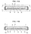
- FIG. 11A and FIG. 11B are views explaining the states when the pressure-contact type semiconductor device shown in FIG. 10A and FIG. 10B is to be used and after it is used for some time, respectively.
- FIG. 11A and FIG. 11B the same reference numerals and symbols are used to designate the same components as those previously explained.
- the metal electrode plates 53, 55 are given a pressure of, for example, several thousands kgf (several ten thousands N) in a facing direction by plates further provided on outer sides thereof.
- the five components namely, the metal electrode plate 53, the heat buffer plates 52, the semiconductor chips 51, the heat buffer plate 54, and the metal electrode plate 55 are brought into an electrically and thermally connected state while being uniformly given the pressure in a compression direction (that is, a uniform pressure-contact state).
- a uniform pressure-contact state that is, a uniform pressure-contact state.
- connecting metal such as solder or the like is not used for electrically connecting the components, satisfactory reliability is obtainable in a thermal cycle repeated when the device is in energizing and when it is not in energizing.
- Heat generated by the semiconductor chips 51 is conveyed through the heat buffer plates 52, 54 and the metal electrode plates 53, 55 and the conveyed heat is heat-exchanged by, for example, water-cooled fins (not shown) provided outside the abovementioned pressure-contact plates. Through this process, the semiconductor device is cooled.
- the heat buffer plates 52, 54 are made to have a thermal expansion coefficient only slightly different from that of silicon which is a main material of the semiconductor chips 51. This reduces a force in a shear direction caused by thermal expansion/contraction which occurs on contact surfaces between the semiconductor chips 51 and the heat buffer plates 52, 54, and makes the electrodes on the front and rear surfaces of the semiconductor chips 51 not liable to break.
- the heat buffer plates 52, 54 for example, molybdenum, tungsten, or the like is usable.
- metal superior in heat conductivity and electrical conductivity for example, copper (plated with, for example, nickel on a surface thereof for oxidation preventive purpose) is used. Copper has a very large thermal expansion coefficient compared with silicon, but since the metal electrode plates 53, 55 are thermally and electrically connected to the semiconductor chips 51 via the heat buffer plates 52, 54, an adverse effect given to the semiconductor chips 51 in the shear direction due to the thermal expansion/contraction of the metal electrode plates 53, 55 is greatly inhibited.
- the pressure contact and heatgeneration cause gradual thermal fatigue of especially the metal electrode plates, resulting in plastic deformation thereof.
- This state is shown in FIG. 11B.
- a peripheral portion 55a of the metal electrode plate 55 bends in a direction of the opposed metal electrode plate 53 and this state becomes a steady state. This is because the heat generation of the semiconductor chips 51 expands the metal electrode plates 55 in the pressure-contact direction so that a bending moment occurs in the peripheral portion 55a thereof not supported by the semiconductor chips 51, the heat buffer plates 52, and the metal electrode plate 55.
- a pressure-contact type semiconductor device includes: a plurality of semiconductor chips; a heat buffer plate provided on one surface side of the plural semiconductor chips; and a metal electrode plate provided on the heat buffer plate on a side opposite the plural semiconductor chips, a surface thereof on the heat buffer plate side being recessed at any position not facing the plural semiconductor chips so as not to be in contact with the heat buffer plate.
- the'principal current mentioned below means not a current flowing through control electrodes but a current flowing between, for example, an anode and a cathode, an emitter and a collector, a source and a drain, and the like.
- Theside face extension' also mentioned below means a side face of the metal electrode plate as a plate and a virtual surface which is formed by extending this side face.
- a pressure-contact type semiconductor device includes: a plurality of semiconductor chips; a heat buffer plate provided on one surface side of the plural semiconductor chips; and a metal electrode plate provided on the heat buffer plate on a side opposite the plural semiconductor chips, a peripheral shape thereof extending beyond and thus being larger than a peripheral shape of the heat buffer plate.
- a pressure-contact type semiconductor device includes: a plurality of semiconductor chips; a heat buffer plate provided on one surface side of the plural semiconductor chips; and a metal electrode plate provided on the heat buffer plate on a side opposite the plural semiconductor chips, a surface thereof at any position not facing the plural semiconductor chips on the heat buffer plate side having a region which alleviates elastic deformation of the heat buffer plate.
- the recession of the metal electrode plate is provided facing a side face extension of this metal electrode plate.
- the pressure-contact type semiconductor device further includes: a plurality of second heat buffer plates provided on the other surface sides of the plural semiconductor chips respectively; and a second metal electrode plate provided on the plural second heat buffer plates on a side opposite the plural semiconductor chips and having projections facing and being in contact with the plural second heat buffer plates respectively and a pedestal portion being a base of the projections.
- the recession of the metal electrode plate is provided slightly outside a position facing the utmost outer projection out of the projections of the second metal electrode plate.
- the metal electrode plate is in contact with the heat buffer plate at positions facing the projections of the second metal electrode plate.
- a peripheral shape of the heat buffer plate falls inside a peripheral shape of the metal electrode plate.
- the heat buffer plate has a shape not extending outside a line connecting utmost outer positions of the plural semiconductor chips.
- the heat buffer plate has a space portion that is provided at a portion thereof not facing the plural semiconductor chips so as to extend in a direction penetrating the heat buffer plate and to reach the metal electrode plate.
- the heat buffer plate has a single plate structure.
- the single plate structure is kept, good assembility can be maintained as a pressure-contact type semiconductor device and deterioration also in terms of maintaining heat conductivity and electrical conductivity can be prevented.
- the heat buffer plate may be constituted of a plurality of plates corresponding to the plural semiconductor chips respectively.
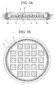
- FIG. 1A and FIG. 1B are schematic views showing the structure of a pressure-contact type semiconductor device according to an embodiment of the present invention.
- FIG. 1A shows a vertical section thereof and
- FIG. 1B is a cross sectional view taken along the A-Aa line in FIG. 1A.
- this pressure-contact type semiconductor device is so structured that a plurality of semiconductor chips 1 in a substantially rectangular shape are arranged in parallel, each having on front and rear surfaces thereof electrodes (not shown) to lead a principal current.
- the semiconductor chips 1,pn junction diodes or switching elements having control terminals such asIGBTs are usable or those in which both are combined are usable.
- the electrode being the control terminal is provided only on a part of the surface on the upper side in FIG. 1A of each of the semiconductor chips 1, and a not-shown conductive material is connected thereto to make the electrode electrically connectable to an external part through an insulative side enclosure 7.
- the semiconductor chips 1 are, for example, 500 ⁇ m in thickness.
- a conductive heat buffer plate 2 On the surface on the upper side in FIG. 1A (the electrode on one side) of each of the semiconductor chips 1, a conductive heat buffer plate 2 is provided, and projections of a metal electrode plate 3 which project from a pedestal portion thereof are in contact with surfaces on a further upper side of the heat buffer plates 2.
- a common conductive heat buffer plate 4 On the surface on the lower side in FIG. 1A (the electrode on the other side) of each of the semiconductor chips 1, a common conductive heat buffer plate 4 is provided, and a metal electrode plate 5 is in contact with a surface on a further lower side of the heat buffer plate 4.
- Each of the heat buffer plates 2 has a thickness of, for example, 1.5 mm
- the heat buffer plate 4 has a thickness of, for example, 2 mm. Note that the shape of the abovementioned projections of the metal electrode plate 3 can be appropriately determined in consideration of plastic deformation caused by pressure-contact and heat generation of the semiconductor chips 1.
- the metal electrode plate 5 is in contact with the heat buffer plate 4 and at the same time, has a portion 5a recessed from a contact surface thereof so as not to be in contact with the heat buffer plate 4.
- This portion 5a not in contact with the heat buffer plate 4 is so formed that it extends from a virtual cylinder surface which is formed by a side face extension of the metal electrode plate 5 and its end reaches the position in the periphery facing the semiconductor chips 1 via the heat buffer plate 4.
- FIG. 2 A top view of the metal electrode plate 5 is shown in FIG. 2.
- FIG. 2 the same reference numerals and symbols are used to designate portions corresponding to those in FIG. 1A and FIG. 1B.
- Each of the metal electrode plate 3, the heat buffer plate 4, and the metal electrode plate 5 has a periphery in a substantially circular shape, and surrounding these peripheries, an insulative side enclosure (made of, for example, ceramic) 7 is provided.
- the side enclosure 7 has a plurality of peripheral projections on an external lateral face thereof to elongate the creeping distance, thereby securing withstand voltage.
- Each of the semiconductor chips 1 further has an insulative resin frame 6 provided in a rim portion thereof on the surface on the upper side in FIG. 1A.
- This resin frame 6 is intended for elongating the creeping distance between both of the electrodes on the semiconductor chips 1, thereby securing withstand voltage.
- the diameter of the metal electrode plate 3 and so on can be, for example, about 10 cm, and as the whole semiconductor device, the rated voltage can be, for example, about several thousands V and the rated current can be, for example, about 1000 A.
- the metal electrode plate 5 is a collector side while the metal electrode plate 3 is an emitter side, and the principal current flows, for example, from the collector side to the emitter side, and when some of the semiconductor chips 1 are used as flywheel diodes, combined with the IGBTs, the upper surface and the lower surface in FIG. 1A of each of the flywheel diodes serve as an anode and a cathode respectively so that a conductive direction therein becomes opposite that in the IGBTs.
- the metal electrode plates 3, 5 are given a pressure of, for example, several thousands kgf (several ten thousands N) in a facing direction by plates further provided on an outer side thereof.
- the five components namely, the metal electrode plate 3, the heat buffer plates 2, the semiconductor chips 1, the heat buffer plate 4, and the metal electrode plate 5 are brought into an electrically and thermally connected state while being uniformly given the pressure in a compression direction. At this time, heat resistance can be reduced.
- Heat generated by the semiconductor chips 1 is conveyed through the heat buffer plates 2, 4 and the metal electrode plates 3, 5 and the conveyed heat is heat-exchanged by, for example, water-cooled fins (not shown) provided outside the abovementioned pressure-contact plates. Through this process, the semiconductor device is cooled.
- the heat buffer plates 2, 4 are made to have a thermal expansion coefficient only slightly different from that of silicon which is a main material of the semiconductor chips 1. This reduces a force in a shear direction caused by thermal expansion/contraction which occurs on contact surfaces between the semiconductor chips 1 and the heat buffer plates 2, 4, and makes the electrodes on the front and rear surfaces of the semiconductor chips 1 not liable to break.
- the heat buffer plates 2, 4 for example, molybdenum, tungsten, or the like is usable.
- metal superior in heat conductivity and electrical conductivity for example, copper (plated with, for example, nickel on a surface thereof for oxidation preventive purpose) is usable. Copper has a very large thermal expansion coefficient compared with silicon, but since the metal electrode plates 3, 5 are thermally and electrically connected to the semiconductor chips 1 via the heat buffer plates 2, 4, an adverse effect given to the semiconductor chips 1 in the shear direction due to the thermal expansion/contraction of the metal electrode plates 3, 5 is greatly inhibited.
- the pressure-contact type semiconductor device as structured above, even when the pressure-contact and heat generation cause gradual thermal fatigue of the metal electrode plate 5, resulting in plastic deformation of a peripheral portion thereof in the direction of the opposed metal electrode plate 3, the influence of the deformation is not given to the heat buffer plate 4. This is because the recessed portion 5a of the metal electrode plate 5 is provided at a portion thereof not facing the semiconductor chips 1 via the heat buffer plate 4 so that the heat buffer plate 4 is not deformed.
- the metal electrode plate 5 can be easily worked into the shape shown in FIG. 2 since the metal electrode plate 5 is made of a comparatively soft material, for example, copper. This is also advantageous in terms of cost and productivity. Incidentally, it is also possible to omit the heat buffer plates 2 on the upper side in FIG. 1A. This is because generally, one surface of the semiconductor chip 1 is easily abraded since a pattern is formed thereon while no pattern is formed on the other surface. It can be thought that the lifetime can be comparatively easily made long even with the abrasion when the surface not having the pattern formed thereon faces the upper side in the drawing.
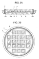
- FIG. 3A and FIG. 3B are schematic views showing the structure of the pressure-contact type semiconductor device according to the other embodiment of the present invention.
- FIG. 3A shows a vertical section thereof and FIG. 3B is a cross sectional view taken along the B-Ba line in FIG. 3A.
- FIG. 3A and FIG. 3B the same reference numerals and symbols are used to designate the same components as those in the drawings previously explained. Duplicate explanation will be omitted below.
- a portion 15a of a metal electrode plate 15 not in contact with a heat buffer plate 4 is made larger than the corresponding portion in the embodiment shown in FIG. 1A and FIG. 1B.
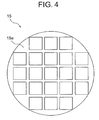
- this portion 15a not in contact with the heat buffer plate 4 is formed in such a manner that it extends from a virtual cylinder face formed by a side face extension of the metal electrode plate 15 and its end reaches the position in the periphery facing semiconductor chips 1 via the heat buffer plate 4, and is provided also in portions between the semiconductor chips 1 that are portions not facing the semiconductor chips 1.
- a top view of the metal electrode plate 15 is shown in FIG. 4.
- FIG. 4 the same reference numerals and symbols are used to designate portions corresponding to those in FIG. 3A and FIG. 3B.
- Other attributes, properties, and so on of the metal electrode plate 15 are the same as those of the metal electrode plate 5 in the embodiment shown in FIG. 1A and FIG. 1B.
- the metal electrode plate 15 can be easily worked into the shape shown in FIG. 4 since the metal electrode plate 15 is made of a comparatively soft material, for example, copper. This is also advantageous in terms of cost and productivity.
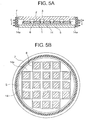
- FIG. 5A and FIG. 5B are schematic views showing the structure of the pressure-contact type semiconductor device according to still another embodiment of the present invention.
- FIG. 5A shows a vertical section thereof and FIG. 5B is a cross sectional view taken along the C-Ca line in FIG. 5A.
- FIG. 5A and FIG. 5B the same reference numerals and symbols are used to designate the same components as those in the drawings previously explained. Duplicate explanation will be omitted below.
- a metal electrode plate 5 has no recessed portion.
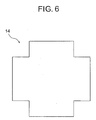
- a heat buffer plate 14 has a space portion 14a provided at a portion thereof not facing semiconductor chips 1, the space portion 14a extending in a direction penetrating the heat buffer plate 14 to reach the metal electrode plate 5.
- the space portion 14a is formed in such a manner that it extends from a virtual cylinder surface formed by a side face extension of the metal electrode plate 5 and its end reaches the position in the periphery facing the semiconductor chips 1.
- a top view of the heat buffer plate 14 is shown in FIG. 6.
- FIG. 6 the same reference numerals and symbols are used to designate portions corresponding to those in FIG. 5A and FIG. 5B.
- Other attributes, properties, and so on of the heat buffer plate 14 are the same as those of the heat buffer plate 4 in the embodiment shown in FIG. 1A and FIG. 1B.
- a plane shape of the heat buffer plate 14 is not circular. Since the heat buffer plate 14 is made of harder metal, workability is inferior to that when it is circular (the embodiments shown in FIG. 1A, FIG. 1B, FIG. 3A, and FIG. 3B), but when the single plate structure is kept, good assembility can be maintained as a semiconductor device.
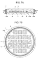
- FIG. 7A and FIG. 7B are schematic views showing the structure of the pressure-contact type semiconductor device according to yet another embodiment of the present invention.
- FIG. 7A shows a vertical section thereof and FIG. 7B is a cross sectional view taken along the D-Da line in FIG. 7A.
- FIG. 7A and FIG. 7B the same reference numerals and symbols are used to designate the same components as those in the drawings previously explained. Duplicate explanation will be omitted below.
- a heat buffer plate 24 constituted not of a single plate but of an aggregate of rectangular plates is used, instead of the heat buffer plate 14 constituted of the single plate shown in FIG. 5A and FIG. 5B.
- workability is better since the shape of each portion of the heat buffer plate 24 is simpler.
- Such a heat buffer plate 24 as the aggregate takes such a form that the heat buffer plate as portions not facing semiconductor chips 1 does not exist, and in this sense, it can be also said that a space portion 24a is made larger than the space portion 14a of the heat buffer plate 14 shown in FIG. 5A and FIG. 5B.
- FIG. 8 A top view of the heat buffer plate 24 as the aggregate is shown in FIG. 8.
- the same reference numerals and symbols are used to designate portions corresponding to those in FIG. 7A and FIG. 7B.
- Other attributes, properties, and so on of the heat buffer plate 24 are the same as those of the heat buffer plate 4 in the embodiment shown in FIG. 1A and FIG. 1B or the heat buffer plate 14 in the embodiment shown in FIG. 5A and FIG. 5B.
- substantially the same effect of enhancing thermal fatigueresistance as that in the embodiment shown in FIG. 5A and FIG. 5B is obtainable.
- it can also cope with the case when a metal electrode plate 5 is softer to be plastically deformed even in portions between the semiconductor chips 1 not facing the semiconductor chips 1 and the plastic deformation may possibly induce elastic deformation of the heat buffer plate.
- the deformation of the heat buffer plate 24 is avoided owing to the space portion 24a.
- FIG. 9A and FIG. 9B are schematic views showing the structure of the pressure-contact type semiconductor device according to yet another embodiment of the present invention.
- FIG. 9A shows a vertical section thereof and FIG. 9B is a cross sectional view taken along the E-Ea line in FIG. 9A.
- FIG. 9A and FIG. 9B the same reference numerals and symbols are used to designate the same components as those in the drawings previously explained. Duplicate explanation will be omitted below.
- a recessed portion (recessed portion 5a) is provided in a metal electrode plate 5 and in addition, a space portion 14a reaching the metal electrode plate 5 is also provided in a heat buffer plate 14 in a portion thereof not facing semiconductor chips 1 in a direction penetrating the heat buffer plate 14.
- the recessed portion 5a of the metal electrode plate 5 is the same as that in the embodiment shown in FIG. 1A and FIG. 1B, and the space portion 14a of the heat buffer plate 14 is the same as that in the embodiment shown in FIG. 5A and FIG. 5B.
Landscapes
- Die Bonding (AREA)
- Cooling Or The Like Of Semiconductors Or Solid State Devices (AREA)
- Thyristors (AREA)
Abstract
Description
Claims (18)
- A pressure-contact type semiconductor device, comprising:a plurality of semiconductor chips;a heat buffer plate provided on one surface side of the plural semiconductor chips; anda metal electrode plate provided on the heat buffer plate on a side opposite the plural semiconductor chips, a surface thereof at any position not facing the plural semiconductor chips on the heat buffer plate side having a region which alleviates elastic deformation of the heat buffer plate.
- A pressure-contact type semiconductor device as set forth in claim 1, wherein the region of the metal electrode plate is recessed so as not to be in contact with the heat buffer plate.
- A pressure-contact type semiconductor device as set forth in claim 2, wherein the recession of the metal electrode plate is provided facing a side face extension of this metal electrode plate.
- A pressure-contact type semiconductor device as set forth in claim 1, further comprising:a plurality of second heat buffer plates provided on the other surface sides of the plural semiconductor chips respectively; anda second metal electrode plate provided on the plural second heat buffer plates on a side opposite the plural semiconductor chip side and having projections facing and being in contact with the plural second heat buffer plates respectively and a pedestal portion being a base of the projections.
- A pressure-contact type semiconductor device as set forth in claim 4, wherein the recession of the metal electrode plate is provided slightly outside a position facing utmost outer projection out of the projections of the second metal electrode plate.
- A pressure-contact type semiconductor device as set forth in claim 4, wherein the metal electrode plate is in contact with the heat buffer plate at positions facing the projections of the second metal electrode plate.
- A pressure-contact type semiconductor device as set forth in claim 1, whereina peripheral shape of the heat buffer plate falls inside a peripheral shape of the metal electrode plate.
- A pressure-contact type semiconductor device as set forth in claim 1, wherein the heat buffer plate has a shape not extending outside a line connecting utmost outer positions of the plural semiconductor chips.
- A pressure-contact type semiconductor device as set forth in claim 1,wherein the heat buffer plate has a space portion that is provided at a portion thereof not facing the plural semiconductor chips so as to extend in a direction penetrating the heat buffer plate and to reach the metal electrode plate.
- A pressure-contact type semiconductor device as set forth in claim 1, wherein the heat buffer plate has a single plate structure.
- A pressure-contact type semiconductor device, comprising:a plurality of semiconductor chips;a heat buffer plate provided on one surface side of the plural semiconductor chips; anda metal electrode plate provided on the heat buffer plate on a side opposite the plural semiconductor chips, a peripheral shape thereof extending beyond and thus being larger than a peripheral shape of the heat buffer plate.
- A pressure-contact type semiconductor device as set forth in claim 11, wherein the heat buffer plate has a shape not extending outside a line connecting utmost outer positions of the plural semiconductor chips.
- A pressure-contact type semiconductor device as set forth in claim 11,wherein the heat buffer plate has a space portion that is provided at a portion thereof not facing the plural semiconductor chips so as to extend in a direction penetrating the heat buffer plate and to reach the metal electrode plate.
- A pressure-contact type semiconductor device as set forth in claim 11, further comprising:a plurality of second heat buffer plates provided on the other surface sides of the plural semiconductor chips respectively; anda second metal electrode plate provided on the plural second heat buffer plates on a side opposite the plural semiconductor chip side and having projections facing and being in contact with the plural second heat buffer plates respectively and a pedestal portion being a base of the projections.
- A pressure-contact type semiconductor device as set forth in claim 14, wherein the metal electrode plate is in contact with the heat buffer plate at positions facing the projections of the second metal electrode plate.
- A pressure-contact type semiconductor device as set forth in claim 14 ,wherein the heat buffer plate has a space portion that is provided at a portion thereof not facing the plural semiconductor chips so as to extend in a direction penetrating the heat buffer plate and to reach the metal electrode plate.
- A pressure-contact type semiconductor device as set forth in claim 11,wherein the heat buffer plate has a single plate structure.
- A pressure-contact type semiconductor device as set forth in claim 11, wherein theheat buffer plate is constituted of a plurality of plates corresponding to the plural semiconductor chips respectively.
Applications Claiming Priority (2)
| Application Number | Priority Date | Filing Date | Title |
|---|---|---|---|
| JP2002180573A JP2004023083A (en) | 2002-06-20 | 2002-06-20 | Pressure welding type semiconductor device |
| JP2002180573 | 2002-06-20 |
Publications (3)
| Publication Number | Publication Date |
|---|---|
| EP1376690A2 true EP1376690A2 (en) | 2004-01-02 |
| EP1376690A3 EP1376690A3 (en) | 2004-01-21 |
| EP1376690B1 EP1376690B1 (en) | 2007-08-01 |
Family
ID=29717522
Family Applications (1)
| Application Number | Title | Priority Date | Filing Date |
|---|---|---|---|
| EP03013356A Expired - Lifetime EP1376690B1 (en) | 2002-06-20 | 2003-06-16 | Pressure-contact type semiconductor device |
Country Status (4)
| Country | Link |
|---|---|
| US (1) | US20040021149A1 (en) |
| EP (1) | EP1376690B1 (en) |
| JP (1) | JP2004023083A (en) |
| DE (1) | DE60315224T2 (en) |
Cited By (5)
| Publication number | Priority date | Publication date | Assignee | Title |
|---|---|---|---|---|
| EP1608015A3 (en) * | 2004-06-09 | 2010-01-13 | Areva T&D Sas | Semiconductor device capsule |
| EP2463899A3 (en) * | 2010-12-07 | 2012-08-08 | SEMIKRON Elektronik GmbH & Co. KG | Semiconductor circuit assembly |
| EP2693473A1 (en) * | 2012-08-03 | 2014-02-05 | GE Energy Power Conversion Technology Ltd | Electronic semiconductor device intended for mounting in a pressed stack assembly, and a pressed stack assembly comprising such a device |
| EP2590213A4 (en) * | 2010-06-30 | 2014-06-11 | Hitachi Automotive Systems Ltd | POWER MODULE AND POWER CONVERTER USING THE SAME |
| EP2966681A1 (en) * | 2014-07-09 | 2016-01-13 | GE Energy Power Conversion Technology Ltd | Power semiconductor devices |
Families Citing this family (8)
| Publication number | Priority date | Publication date | Assignee | Title |
|---|---|---|---|---|
| JP2005094842A (en) * | 2003-09-12 | 2005-04-07 | Toshiba Corp | Inverter device and manufacturing method thereof |
| JP5936579B2 (en) * | 2013-05-08 | 2016-06-22 | 本田技研工業株式会社 | Current application device |
| US9728517B2 (en) * | 2013-12-17 | 2017-08-08 | Taiwan Semiconductor Manufacturing Company Ltd. | Semiconductor device and manufacturing method thereof |
| JP6386936B2 (en) * | 2015-02-26 | 2018-09-05 | 京セラ株式会社 | Method of manufacturing electrode member for pressure contact type semiconductor device |
| EP3324432A1 (en) * | 2016-11-17 | 2018-05-23 | Infineon Technologies AG | Method of electrically contacting a plurality of semiconductor chips |
| CN110416187B (en) * | 2019-06-28 | 2021-07-09 | 西安中车永电电气有限公司 | A new type of crimp IGBT internal packaging structure |
| CN113053831B (en) * | 2019-12-27 | 2023-09-05 | 株洲中车时代半导体有限公司 | A crimping type IGBT module and power semiconductor device |
| JP7395452B2 (en) * | 2020-09-23 | 2023-12-11 | 株式会社東芝 | semiconductor equipment |
Family Cites Families (9)
| Publication number | Priority date | Publication date | Assignee | Title |
|---|---|---|---|---|
| JP3258200B2 (en) * | 1995-05-31 | 2002-02-18 | 株式会社東芝 | Pressure contact type semiconductor device |
| JPH081914B2 (en) * | 1987-03-31 | 1996-01-10 | 株式会社東芝 | Pressure contact type semiconductor device |
| JPH04352457A (en) * | 1991-05-30 | 1992-12-07 | Mitsubishi Electric Corp | Semiconductor device and manufacture thereof |
| JP3256636B2 (en) * | 1994-09-15 | 2002-02-12 | 株式会社東芝 | Pressure contact type semiconductor device |
| JP3588503B2 (en) * | 1995-06-20 | 2004-11-10 | 株式会社東芝 | Pressure welding type semiconductor device |
| JP3344552B2 (en) * | 1997-09-17 | 2002-11-11 | 株式会社東芝 | Pressure welding type semiconductor device |
| CN1236982A (en) * | 1998-01-22 | 1999-12-01 | 株式会社日立制作所 | Pressure contact type semiconductor device and its converter |
| JP2930074B1 (en) * | 1998-06-02 | 1999-08-03 | 富士電機株式会社 | Semiconductor device |
| DE10048436A1 (en) * | 2000-09-29 | 2002-04-18 | Siemens Ag | Electronic switch for heavy currents at high voltage and low temperatures comprises parallel FET power semiconductors between pressure plates |
-
2002
- 2002-06-20 JP JP2002180573A patent/JP2004023083A/en not_active Abandoned
-
2003
- 2003-06-13 US US10/460,414 patent/US20040021149A1/en not_active Abandoned
- 2003-06-16 EP EP03013356A patent/EP1376690B1/en not_active Expired - Lifetime
- 2003-06-16 DE DE60315224T patent/DE60315224T2/en not_active Expired - Lifetime
Cited By (7)
| Publication number | Priority date | Publication date | Assignee | Title |
|---|---|---|---|---|
| EP1608015A3 (en) * | 2004-06-09 | 2010-01-13 | Areva T&D Sas | Semiconductor device capsule |
| EP2590213A4 (en) * | 2010-06-30 | 2014-06-11 | Hitachi Automotive Systems Ltd | POWER MODULE AND POWER CONVERTER USING THE SAME |
| EP2463899A3 (en) * | 2010-12-07 | 2012-08-08 | SEMIKRON Elektronik GmbH & Co. KG | Semiconductor circuit assembly |
| EP2693473A1 (en) * | 2012-08-03 | 2014-02-05 | GE Energy Power Conversion Technology Ltd | Electronic semiconductor device intended for mounting in a pressed stack assembly, and a pressed stack assembly comprising such a device |
| FR2994333A1 (en) * | 2012-08-03 | 2014-02-07 | Ge Energy Power Conversion Technology Ltd | SEMICONDUCTOR ELECTRONIC DEVICE FOR MOUNTING IN A PRESSED STACK ASSEMBLY AND PRESSED STACK ASSEMBLY COMPRISING SUCH A DEVICE |
| US9093426B2 (en) | 2012-08-03 | 2015-07-28 | Ge Energy Power Conversion Technology Ltd. | Electronic semi-conductor device intended for mounting in a pressed stack assembly, and a pressed stack assembly comprising such device |
| EP2966681A1 (en) * | 2014-07-09 | 2016-01-13 | GE Energy Power Conversion Technology Ltd | Power semiconductor devices |
Also Published As
| Publication number | Publication date |
|---|---|
| DE60315224D1 (en) | 2007-09-13 |
| US20040021149A1 (en) | 2004-02-05 |
| DE60315224T2 (en) | 2008-04-17 |
| JP2004023083A (en) | 2004-01-22 |
| EP1376690A3 (en) | 2004-01-21 |
| EP1376690B1 (en) | 2007-08-01 |
Similar Documents
| Publication | Publication Date | Title |
|---|---|---|
| US8736043B2 (en) | Power device having a specific range of distances between collector and emitter electrodes | |
| US6181007B1 (en) | Semiconductor device | |
| US20120244697A1 (en) | Method for fabricating a semiconductor device | |
| US20030075783A1 (en) | Semiconductor device | |
| EP1376690B1 (en) | Pressure-contact type semiconductor device | |
| JP7060104B2 (en) | Semiconductor device | |
| EP0702406A2 (en) | Press-contact type semiconductor devices | |
| JP2011036016A (en) | Power converter | |
| JP2002198477A (en) | Semiconductor device | |
| CN111542921B (en) | Semiconductor device | |
| US11688711B2 (en) | Semiconductor device having second connector that overlaps a part of first connector | |
| JP2013191806A (en) | Semiconductor device and method for manufacturing the same | |
| JP5904041B2 (en) | Semiconductor device | |
| JP2012124247A (en) | Joint element, method of manufacturing semiconductor device and semiconductor device | |
| US6445013B1 (en) | Gate commutated turn-off semiconductor device | |
| EP3907756A1 (en) | Power module of double-faced cooling and manufacturing method thereof | |
| JP3973832B2 (en) | Pressure contact type semiconductor device | |
| US20230197561A1 (en) | Power semiconductor module comprising a substrate, power semiconductor components and comprising a pressure body | |
| WO2018029801A1 (en) | Semiconductor device | |
| JP2000012845A (en) | Semiconductor device | |
| JP4458028B2 (en) | Semiconductor device | |
| JP5724415B2 (en) | Semiconductor module | |
| US20250391803A1 (en) | Method for producing a semiconductor assembly comprising a semiconductor element and a substrate, and corresponding device | |
| JP7722864B2 (en) | Semiconductor Devices | |
| US10847489B2 (en) | Semiconductor device |
Legal Events
| Date | Code | Title | Description |
|---|---|---|---|
| PUAI | Public reference made under article 153(3) epc to a published international application that has entered the european phase |
Free format text: ORIGINAL CODE: 0009012 |
|
| PUAL | Search report despatched |
Free format text: ORIGINAL CODE: 0009013 |
|
| 17P | Request for examination filed |
Effective date: 20030616 |
|
| AK | Designated contracting states |
Kind code of ref document: A2 Designated state(s): AT BE BG CH CY CZ DE DK EE ES FI FR GB GR HU IE IT LI LU MC NL PT RO SE SI SK TR |
|
| AX | Request for extension of the european patent |
Extension state: AL LT LV MK |
|
| AK | Designated contracting states |
Kind code of ref document: A3 Designated state(s): AT BE BG CH CY CZ DE DK EE ES FI FR GB GR HU IE IT LI LU MC NL PT RO SE SI SK TR |
|
| AX | Request for extension of the european patent |
Extension state: AL LT LV MK |
|
| RIC1 | Information provided on ipc code assigned before grant |
Ipc: 7H 01L 23/13 B Ipc: 7H 01L 23/48 A |
|
| 17Q | First examination report despatched |
Effective date: 20040311 |
|
| AKX | Designation fees paid |
Designated state(s): CH DE IT LI |
|
| RIC1 | Information provided on ipc code assigned before grant |
Ipc: H01L 23/00 20060101ALI20061121BHEP Ipc: H01L 23/051 20060101ALI20061121BHEP Ipc: H01L 23/48 20060101AFI20061121BHEP Ipc: H01L 23/13 20060101ALI20061121BHEP Ipc: H01L 25/07 20060101ALI20061121BHEP |
|
| GRAP | Despatch of communication of intention to grant a patent |
Free format text: ORIGINAL CODE: EPIDOSNIGR1 |
|
| GRAS | Grant fee paid |
Free format text: ORIGINAL CODE: EPIDOSNIGR3 |
|
| GRAA | (expected) grant |
Free format text: ORIGINAL CODE: 0009210 |
|
| AK | Designated contracting states |
Kind code of ref document: B1 Designated state(s): CH DE IT LI |
|
| REG | Reference to a national code |
Ref country code: CH Ref legal event code: EP |
|
| REF | Corresponds to: |
Ref document number: 60315224 Country of ref document: DE Date of ref document: 20070913 Kind code of ref document: P |
|
| REG | Reference to a national code |
Ref country code: CH Ref legal event code: NV Representative=s name: E. BLUM & CO. AG PATENT- UND MARKENANWAELTE VSP |
|
| PLBE | No opposition filed within time limit |
Free format text: ORIGINAL CODE: 0009261 |
|
| STAA | Information on the status of an ep patent application or granted ep patent |
Free format text: STATUS: NO OPPOSITION FILED WITHIN TIME LIMIT |
|
| 26N | No opposition filed |
Effective date: 20080506 |
|
| PGFP | Annual fee paid to national office [announced via postgrant information from national office to epo] |
Ref country code: IT Payment date: 20160621 Year of fee payment: 14 |
|
| PG25 | Lapsed in a contracting state [announced via postgrant information from national office to epo] |
Ref country code: IT Free format text: LAPSE BECAUSE OF NON-PAYMENT OF DUE FEES Effective date: 20170616 |
|
| PGFP | Annual fee paid to national office [announced via postgrant information from national office to epo] |
Ref country code: DE Payment date: 20220420 Year of fee payment: 20 |
|
| PGFP | Annual fee paid to national office [announced via postgrant information from national office to epo] |
Ref country code: CH Payment date: 20220702 Year of fee payment: 20 |
|
| REG | Reference to a national code |
Ref country code: DE Ref legal event code: R071 Ref document number: 60315224 Country of ref document: DE |
|
| REG | Reference to a national code |
Ref country code: CH Ref legal event code: PL |