EP1376683A1 - Process for forming trenches with oblique profile and rounded top corners - Google Patents
Process for forming trenches with oblique profile and rounded top corners Download PDFInfo
- Publication number
- EP1376683A1 EP1376683A1 EP02425428A EP02425428A EP1376683A1 EP 1376683 A1 EP1376683 A1 EP 1376683A1 EP 02425428 A EP02425428 A EP 02425428A EP 02425428 A EP02425428 A EP 02425428A EP 1376683 A1 EP1376683 A1 EP 1376683A1
- Authority
- EP
- European Patent Office
- Prior art keywords
- process according
- etch
- wafer
- polymerizing
- voltage
- Prior art date
- Legal status (The legal status is an assumption and is not a legal conclusion. Google has not performed a legal analysis and makes no representation as to the accuracy of the status listed.)
- Granted
Links
Images


Classifications
-
- H—ELECTRICITY
- H10—SEMICONDUCTOR DEVICES; ELECTRIC SOLID-STATE DEVICES NOT OTHERWISE PROVIDED FOR
- H10W—GENERIC PACKAGES, INTERCONNECTIONS, CONNECTORS OR OTHER CONSTRUCTIONAL DETAILS OF DEVICES COVERED BY CLASS H10
- H10W10/00—Isolation regions in semiconductor bodies between components of integrated devices
- H10W10/10—Isolation regions comprising dielectric materials
- H10W10/17—Isolation regions comprising dielectric materials formed using trench refilling with dielectric materials, e.g. shallow trench isolations
-
- H—ELECTRICITY
- H10—SEMICONDUCTOR DEVICES; ELECTRIC SOLID-STATE DEVICES NOT OTHERWISE PROVIDED FOR
- H10P—GENERIC PROCESSES OR APPARATUS FOR THE MANUFACTURE OR TREATMENT OF DEVICES COVERED BY CLASS H10
- H10P50/00—Etching of wafers, substrates or parts of devices
- H10P50/20—Dry etching; Plasma etching; Reactive-ion etching
- H10P50/24—Dry etching; Plasma etching; Reactive-ion etching of semiconductor materials
- H10P50/242—Dry etching; Plasma etching; Reactive-ion etching of semiconductor materials of Group IV materials
-
- H—ELECTRICITY
- H10—SEMICONDUCTOR DEVICES; ELECTRIC SOLID-STATE DEVICES NOT OTHERWISE PROVIDED FOR
- H10P—GENERIC PROCESSES OR APPARATUS FOR THE MANUFACTURE OR TREATMENT OF DEVICES COVERED BY CLASS H10
- H10P50/00—Etching of wafers, substrates or parts of devices
- H10P50/69—Etching of wafers, substrates or parts of devices using masks for semiconductor materials
- H10P50/691—Etching of wafers, substrates or parts of devices using masks for semiconductor materials for Group V materials or Group III-V materials
- H10P50/693—Etching of wafers, substrates or parts of devices using masks for semiconductor materials for Group V materials or Group III-V materials characterised by their size, orientation, disposition, behaviour or shape, in horizontal or vertical plane
- H10P50/695—Etching of wafers, substrates or parts of devices using masks for semiconductor materials for Group V materials or Group III-V materials characterised by their size, orientation, disposition, behaviour or shape, in horizontal or vertical plane characterised by the process involved to create the mask, e.g. lift-off masks or sidewalls or to modify the mask
-
- H—ELECTRICITY
- H10—SEMICONDUCTOR DEVICES; ELECTRIC SOLID-STATE DEVICES NOT OTHERWISE PROVIDED FOR
- H10W—GENERIC PACKAGES, INTERCONNECTIONS, CONNECTORS OR OTHER CONSTRUCTIONAL DETAILS OF DEVICES COVERED BY CLASS H10
- H10W10/00—Isolation regions in semiconductor bodies between components of integrated devices
- H10W10/01—Manufacture or treatment
- H10W10/011—Manufacture or treatment of isolation regions comprising dielectric materials
- H10W10/014—Manufacture or treatment of isolation regions comprising dielectric materials using trench refilling with dielectric materials, e.g. shallow trench isolations
- H10W10/0145—Manufacture or treatment of isolation regions comprising dielectric materials using trench refilling with dielectric materials, e.g. shallow trench isolations of trenches having shapes other than rectangular or V-shape
Definitions
- the present invention relates to a process for forming trenches with oblique profile and rounded top corners.
- STI shallow-trench isolation
- STI shallow-trench isolation
- a trench of preset width and depth is initially opened; then, the trench is filled with silicon oxide or with another dielectric material.
- the trench is normally dug by dry plasma etching, which is markedly anisotropic.
- the walls of the trench can in some cases be vertical, but frequently the geometrical and electrical characteristics of the circuits require the trench to have an oblique profile and the walls to be inclined, for example by an angle of between 65° and 85° ( «tapered trench»).
- This solution makes it possible, for example, to prevent the electric field lines from crowding near over-pronounced corners, so creating potentially dangerous situations.
- TCR top-corner rounding
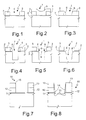
- FIG. 1 A first known process for forming trenches provided with rounded top corners will be illustrated with reference to Figures 1-6.
- a semiconductor wafer 1 is initially coated with a pad oxide layer 2 and with an stop layer 3 of silicon nitride having openings 4 obtained with conventional lithographic techniques ( Figure 1).
- the stop layer 3 is to be used for subsequent steps of planarization of the wafer 1.
- a thick oxide layer 5 is deposited so as to coat the stop layer 3 ( Figure 2) and is then defined so as to form spacers 6 inside the openings 4 ( Figure 3).
- the spacers 6 occupy peripheral portions of the openings 4, leaving central portions uncovered.
- a trench 7 with a preset profile is then opened ( Figure 4) and, with a wet etch, the spacers 6 and portions of the pad oxide layer 2 inside the openings 4 are then removed (Figure 5). Now, the trench 7 is upwardly delimited by top corners 8 having edges 9. By a further dry etch, the edges 9 are tapered, so as to obtain rounded top corners 8'.
- the described process is not, however, free from limitations.
- the dry etch for rounding off the edges 9 inevitably also involves the walls of the trench 7, the profile of which is modified in an uncontrollable way.
- This undesired effect is disadvantageous, since the electrical properties of an insulating structure depend, in general, also upon its shape.
- numerous processing steps are necessary, in particular, a greater number of alternate plasma and wet etching steps.
- the method is costly and complex to be implemented, and the risk of generating crystallographic defects is not satisfactorily small.
- the wafer must be handled and displaced a number of times between different machines: the wafer thus remains exposed to dust and other impurities that can cause defects or damage of varying degree.
- a different process illustrated with reference to Figures 7-10, provides forming a pad oxide layer 11 and a stop layer 12 on top of a wafer 10, as already described.
- the stop layer 12 is defined using a resist mask 13.
- Figure 8 uncovered portions of the pad oxide layer 11 and portions of silicon immediately underneath are removed through an anisotropic etch with inclined profile, in particular a polymerizing dry etch.
- this type of etching is performed in particular conditions, whereby, simultaneously with removing material from the wafer 1, the compounds present in the plasma are microdeposited.
- the rate of microdeposition is higher than the rate of etching and consequently a protective polymeric film 14 progressively grows around the portions with high constant slope.
- a second polymeric film 17 is formed, which, however, does not grow in a regular way: at the start of the process and in the proximity of the polymeric film 14, the growth of the second polymeric film 17 is more rapid and slows down as the trench 16' is dug.
- a crowned, substantially cusp-shaped, profile is obtained, as shown in Figure 10b.
- the cusp-shaped profile is not satisfactory, both because it requires the devices to be designed taking into account complex phenomena, due precisely to the constant non-constant slope of the walls of the trench 16', and, above all, because it causes various problems in the subsequent processing steps.
- the filling of the trench 16' is problematical and thus is frequently imperfect; in the thermal treatment, the portions of the wafer 10' surrounding the trench 16' are subjected to extremely strong mechanical stresses; in addition, crystallographic defects may be formed, especially on the bottom of the trench 16'.
- the aim of the present invention is to provide a process for forming insulating structures that is free from the drawbacks described above.
- a process is provided for forming insulating structures with an oblique profile and rounded top corners, as defined in claim 1.
- a wafer 20 of semiconductor material for example monocrystalline silicon, comprises a substrate 21, on which a pad oxide layer 22 is initially grown.
- a stop layer 23 is then formed, which is to be used for subsequent planarization of the wafer 20.
- the stop layer 23 has openings 25 uncovering portions 22' of the pad oxide layer 22; in particular the portions 22' rise above regions of the substrate 21 that are subsequently to be etched.
- the stop layer 23 is formed using a resist mask 26, which is deposited and then defined photolithographically.
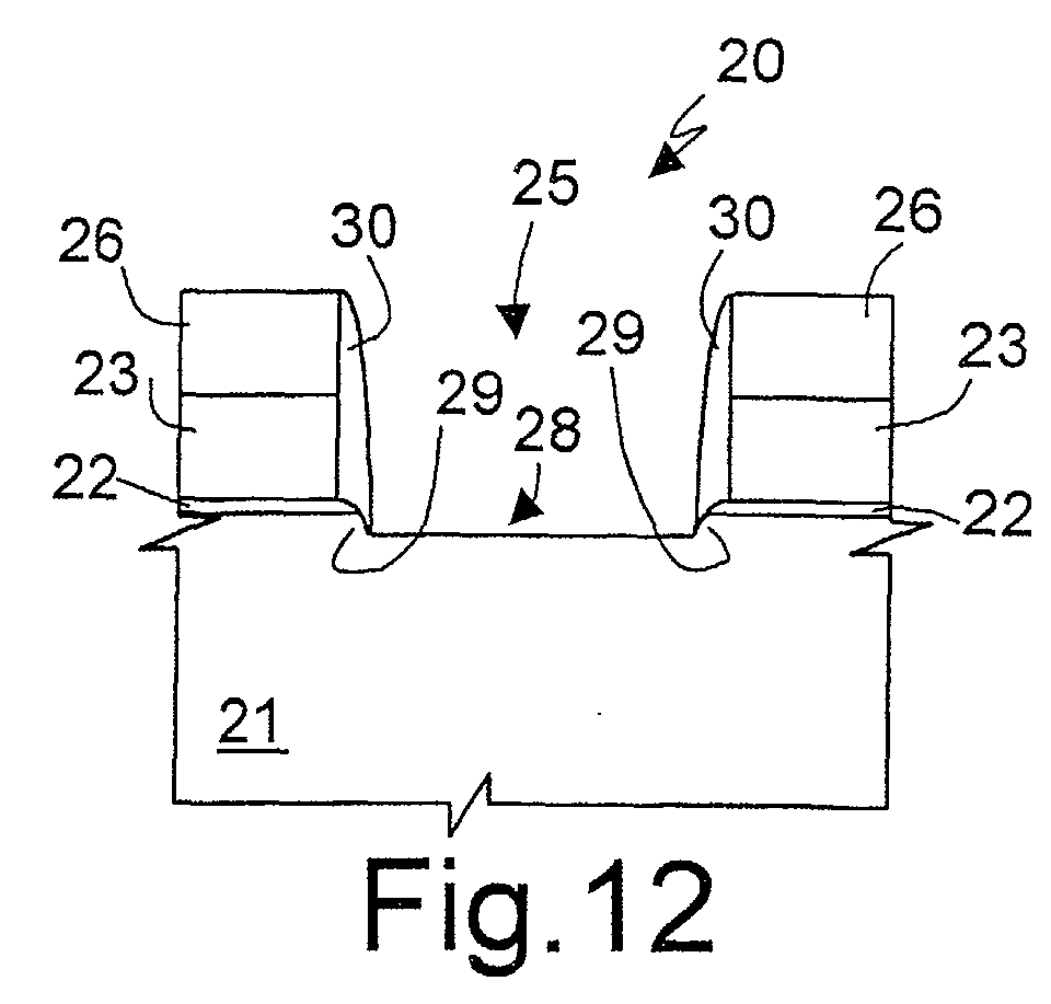
- a first dry polymerizing etch is carried out, as shown in Figure 12.
- the polymerizing etch is a plasma etch, preferably a CHF 3 - or CH 2 F 2 -based etch.
- the portions 22' of the pad oxide layer 22 are removed, and the underlying silicon is slightly dug so as to form depressions 28.
- a first polymeric film 30 is formed, which gradually grows in thickness towards the inside of the openings 25.
- the exposed surface of the pad oxide layer 22 first and that of the substrate 21 next decreases, starting from the periphery. Consequently, with the passage of time the etch involves an increasingly restricted central area, which is dug more deeply at the bottom than at the peripheral areas. In this way, rounded top corners 29 are formed, which delimit the depressions 28.
- a second dry polymerizing etch is then performed to open a trench 31 ( Figures 13-15).
- the second polymerizing etch is a markedly anisotropic plasma etch, preferably HBr- and O 2 -based; in addition, the etch can be made in presence of Cl 2 and N 2 .
- the second polymerizing etch is performed in variable plasma conditions.
- plasma etching is performed by placing the wafer 20 in an etching chamber 32, in which a known mixture of gases flows in predetermined conditions of temperature, pressure and flow ( Figure 16).
- the etching chamber 32 is set at a chamber voltage V C , while the wafer 20 is kept at a wafer voltage V W .
- the rate of removal of the silicon and the rate of microdeposition of the polymeric material of the plasma are affected by various parameters, among which the etching voltage V E . In particular, all other conditions being equal, the rate of microdeposition increases as the absolute value of the etching voltage V E increases.
- the second polymerizing etch is performed in discrete steps and comprises a number N of steps performed in succession. As shown in Figure 17, associated to the etching steps are respective durations T 1 , T 2 , ..., T N and respective increasing values V E1 , V E2 , ..., V EN of the etching voltage V E .
- the second polymerizing etch can comprise three steps, each having a duration of 30 s. Furthermore, for each step the value of the etching voltage V E is obtained by keeping the chamber voltage V C constant (for example at 0 V) and imposing values of the wafer voltage V W of 10 V, 20 V and 30 V, respectively. Thereby, a discrete-ramp etching voltage V E is supplied. The etching steps are moreover performed one after the other, in rapid succession, substantially without interruptions.
- the variations in the growth rate of the second polymerizing film 33 caused by the presence of the first polymerizing film 30 are compensated, in particular near the exposed surface 36 of the substrate 21.
- the growth of the second polymeric film is rapid because, in addition to the effect due to the etching voltage V E , the presence of the first polymeric film 30 has a significant effect.
- the first polymeric film 30 is initially contiguous to the exposed surface 36 that is etched.
- the etching voltage V E is varied as already explained with reference to Figure 17, so that the variations in the microdeposition rate of polymeric material and in the removal rate of silicon will make up for the different effect caused by the first polymeric film 30.
- Figure 15 shows the wafer 20 at the end of the second polymerizing etch: it is possible to identify the trench 31, delimited by the walls 37 with a constant slope ⁇ and the first and the second polymeric films 30, 33.
- the walls 37 constantly form an angle with respect to a surface parallel to a face 38 of the substrate 21.
- the angle ⁇ is between 65° and 85° and, for example, is 80°.
- the first and the second polymeric films 30, 33 and the resist mask 26 are removed simultaneously with a single step of wet washing ( Figure 18).
- a dielectric material preferably silicon oxide
- the trench 31 is then completely filled with a dielectric material, preferably silicon oxide, so as to form an insulating structure 40 extending in the substrate 21 for the entire depth of the trench 31 ( Figure 19).
- a dielectric material preferably silicon oxide
- Excess portions of silicon oxide, the stop layer 23, and the pad oxide layer 22 are then removed after planarization of the wafer 20.
- the processing of the wafer 20 is then completed with standard steps for forming integrated circuits 41, represented schematically in Figure 20 by the symbols of active and passive electronic components.
- the integrated circuits 41 are made inside active areas 42 of the wafer 20 delimited by adjacent insulating structures 40.
- the etching voltage V E is varied continuously according to a linear ramp, as shown in Figure 21. Also in this case, the wafer voltage V W is controlled so as to obtain the desired etching voltage V E .
- a third embodiment of the invention provides for varying the composition of the plasma used during the second polymerizing etch.
- at least two gases are present in the plasma: a first gas, for example HBr or Cl 2 , is used for etching the substrate 21, while a second gas, for example O 2 , HeO 2 or N 2 , brings about polymerization and microdeposition of polymeric material.
- a first gas for example HBr or Cl 2
- a second gas for example O 2 , HeO 2 or N 2
- the concentration C of the polymerizing gas present in the mixture is varied.
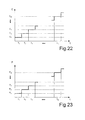
- the concentration C is increased according to a discrete-ramp pattern, as illustrated in Figure 22.
- the pressure P of the plasma is modified, also in this case according to a discrete-ramp pattern (see Figure 23).
- the process described is advantageous mainly because it enables insulating structures to be made with inclined walls having a constant slope and at the same time provided with rounded top corners. It is therefore possible to exploit the advantages of the TCR technique also in the numerous cases where it is necessary to dig trenches with an oblique profile. In particular, it is possible to define active areas of high quality, to reduce the parasitic effects within the active areas. In addition, the use of the TCR technique for digging trenches reduces the risk of any crystallographic defects being generated in subsequent processing steps, especially during thermal treatment. In practice, then, both the yield of the process and the quality of the devices that can be made in the active areas improve considerably.
- the etching voltage may present a parabolic curve, either a continuous one or a discrete one, or even of some other type.
- the increments of the etching voltage might not be uniform.
- the various steps of the second polymerizing etch may also have different durations.
Landscapes
- Drying Of Semiconductors (AREA)
- Element Separation (AREA)
Abstract
Description
- The present invention relates to a process for forming trenches with oblique profile and rounded top corners.
- As is known, in microelectronics there is an ever increasing need to reduce the overall dimensions of integrated circuits. Clearly, to achieve this aim, it is necessary, on the one hand, to optimize the number of electronic components to be made and, on the other, to minimize the size of the components and, in general, of all the structures that cooperate in the operation of the integrated circuit.
- The reduction of the size causes, however, difficulties, for example, in forming insulating structures that separate adjacent active areas, and it is therefore necessary to adopt particular solutions.
- For example, so-called shallow-trench isolation (STI) structures are compatible with the use of technologies that enable the fabrication of active devices of length smaller than 0.25 µm. To form the insulating structures, in a wafer of semiconductor material a trench of preset width and depth is initially opened; then, the trench is filled with silicon oxide or with another dielectric material. The trench is normally dug by dry plasma etching, which is markedly anisotropic. The walls of the trench can in some cases be vertical, but frequently the geometrical and electrical characteristics of the circuits require the trench to have an oblique profile and the walls to be inclined, for example by an angle of between 65° and 85° («tapered trench»). This solution makes it possible, for example, to prevent the electric field lines from crowding near over-pronounced corners, so creating potentially dangerous situations.
- In order to improve the insulating structures of an STI type, it has been proposed to provide the trenches with rounded top corners, using the top-corner rounding (TCR) technique. This technique chiefly provides two advantages: first, the space available for forming active areas increases and, second, the likelihood of the subsequent processing steps causing crystallographic defects is reduced.
- A first known process for forming trenches provided with rounded top corners will be illustrated with reference to Figures 1-6. According to this process, a
semiconductor wafer 1 is initially coated with apad oxide layer 2 and with anstop layer 3 of silicon nitride having openings 4 obtained with conventional lithographic techniques (Figure 1). Thestop layer 3 is to be used for subsequent steps of planarization of thewafer 1. Then, athick oxide layer 5 is deposited so as to coat the stop layer 3 (Figure 2) and is then defined so as to formspacers 6 inside the openings 4 (Figure 3). In greater detail, thespacers 6 occupy peripheral portions of the openings 4, leaving central portions uncovered. By anisotropic plasma etching, atrench 7 with a preset profile is then opened (Figure 4) and, with a wet etch, thespacers 6 and portions of thepad oxide layer 2 inside the openings 4 are then removed (Figure 5). Now, thetrench 7 is upwardly delimited bytop corners 8 havingedges 9. By a further dry etch, theedges 9 are tapered, so as to obtain rounded top corners 8'. - The described process is not, however, free from limitations. First, the dry etch for rounding off the
edges 9 inevitably also involves the walls of thetrench 7, the profile of which is modified in an uncontrollable way. This undesired effect is disadvantageous, since the electrical properties of an insulating structure depend, in general, also upon its shape. Clearly, it is difficult, if not impossible, to foresee accurately the electrical interactions between the insulating structure obtainable by filling in thetrench 7 and the devices that are to be made in thewafer 1. These interactions can render the behavior of the devices integrated in the wafer significantly different from the design, both as regards performance and as regards safety margins for protection from any possible failure. In addition, numerous processing steps are necessary, in particular, a greater number of alternate plasma and wet etching steps. Consequently, the method is costly and complex to be implemented, and the risk of generating crystallographic defects is not satisfactorily small. Instead, on account of the high number and of the type of operations to be performed, the wafer must be handled and displaced a number of times between different machines: the wafer thus remains exposed to dust and other impurities that can cause defects or damage of varying degree. - A different process, illustrated with reference to Figures 7-10, provides forming a
pad oxide layer 11 and astop layer 12 on top of awafer 10, as already described. In particular, thestop layer 12 is defined using aresist mask 13. Then (Figure 8), uncovered portions of thepad oxide layer 11 and portions of silicon immediately underneath are removed through an anisotropic etch with inclined profile, in particular a polymerizing dry etch. As is known, this type of etching is performed in particular conditions, whereby, simultaneously with removing material from thewafer 1, the compounds present in the plasma are microdeposited. On the vertical or markedly inclined walls, the rate of microdeposition is higher than the rate of etching and consequently a protectivepolymeric film 14 progressively grows around the portions with high constant slope. Starting from the periphery, the horizontal surface exposed to etching gradually reduces over time; in this way, roundedtop corners 15 are obtained, as shown in Figure 8. Finally, atrench 16 is opened through a further dry anisotropic etch (Figure 9), and theresist mask 13 and thepolymeric film 14 are removed (Figure 10a). - The process described above, however, has a considerable limitation, in so far as it does not enable trenches with an oblique profile to be formed, but only ones with vertical profile. To obtain an oblique profile, in fact, it is necessary to perform a further polymerizing dry etch, using a polymer that is very different from the previous one. In addition, the trench is opened before removing the polymeric film formed during the first dry etch, which is thus still present. In practice, the polymeric film affects the evolution of the second dry etch, inducing different rates of polymerization according to the depth reached inside the
wafer 10. In greater detail, during the second dry etch a secondpolymeric film 17 is formed, which, however, does not grow in a regular way: at the start of the process and in the proximity of thepolymeric film 14, the growth of the secondpolymeric film 17 is more rapid and slows down as the trench 16' is dug. In practice, then, a crowned, substantially cusp-shaped, profile is obtained, as shown in Figure 10b. The cusp-shaped profile is not satisfactory, both because it requires the devices to be designed taking into account complex phenomena, due precisely to the constant non-constant slope of the walls of the trench 16', and, above all, because it causes various problems in the subsequent processing steps. In particular, the filling of the trench 16' is problematical and thus is frequently imperfect; in the thermal treatment, the portions of the wafer 10' surrounding the trench 16' are subjected to extremely strong mechanical stresses; in addition, crystallographic defects may be formed, especially on the bottom of the trench 16'. - Alternatively, it is possible to remove the
polymeric film 14 formed during the first polymerizing etch before performing the second etch. However, the complete removal of the film grown during a polymerizing etch is problematical and requires a wet washing of the wafer, which, however, causes complete removal of the residual resist. The subsequent etches would thus have a very limited polymerizing power (the polymer comes, in fact, to a great extent from the products of etching of the photoresist), preventing in practice the obtainment of the desired oblique profile. In addition, this solution involves picking up the wafer, setting it in a different machine, carrying out washing, and re-positioning of the wafer to carry out the second plasma etch. All these steps must evidently be repeated to remove thefilms - The aim of the present invention is to provide a process for forming insulating structures that is free from the drawbacks described above.
- According to the present invention a process is provided for forming insulating structures with an oblique profile and rounded top corners, as defined in
claim 1. - For a better understanding of the invention, some embodiments thereof are now described, purely by way of non-limiting examples and with reference to the attached drawings, wherein:
- Figures 1-6 are cross-sections through a semiconductor wafer in successive processing steps, according to a known process;
- Figures 7-10b are cross-sections through semiconductor wafers in successive processing steps, according to a different known process;
- Figures 11-15 are cross-sections through a semiconductor wafer in successive processing steps of the process according to the present invention;
- Figure 16 is a schematic view of an apparatus used in one step of the process according to the present invention;
- Figure 17 is the plot of a quantity regarding the present process;
- Figures 18-20 are cross-sections of the wafer of Figures 11-15, in subsequent processing steps; and
- Figures 21-23 are plots of quantities regarding, respectively, a second, a third, and a fourth embodiment of the process according to the present invention.
- With reference to Figures 11-20, a
wafer 20 of semiconductor material, for example monocrystalline silicon, comprises asubstrate 21, on which apad oxide layer 22 is initially grown. On top of the pad oxide layer 22 astop layer 23 is then formed, which is to be used for subsequent planarization of thewafer 20. Thestop layer 23 hasopenings 25 uncovering portions 22' of thepad oxide layer 22; in particular the portions 22' rise above regions of thesubstrate 21 that are subsequently to be etched. Thestop layer 23 is formed using aresist mask 26, which is deposited and then defined photolithographically. - Then, a first dry polymerizing etch is carried out, as shown in Figure 12. The polymerizing etch is a plasma etch, preferably a CHF3- or CH2F2-based etch. In detail, in this step, the portions 22' of the
pad oxide layer 22 are removed, and the underlying silicon is slightly dug so as to formdepressions 28. During the polymerizing etch, on thesurface 23a of thehard mask 23 and on thesurface 26a of theresist mask 26 delimiting the openings 25 a firstpolymeric film 30 is formed, which gradually grows in thickness towards the inside of theopenings 25. As the thickness of thefirst polymerizing film 30 increases, the exposed surface of thepad oxide layer 22 first and that of thesubstrate 21 next decreases, starting from the periphery. Consequently, with the passage of time the etch involves an increasingly restricted central area, which is dug more deeply at the bottom than at the peripheral areas. In this way, roundedtop corners 29 are formed, which delimit thedepressions 28. - A second dry polymerizing etch is then performed to open a trench 31 (Figures 13-15). The second polymerizing etch is a markedly anisotropic plasma etch, preferably HBr- and O2-based; in addition, the etch can be made in presence of Cl2 and N2. The second polymerizing etch is performed in variable plasma conditions. In greater detail, plasma etching is performed by placing the
wafer 20 in anetching chamber 32, in which a known mixture of gases flows in predetermined conditions of temperature, pressure and flow (Figure 16). In addition, theetching chamber 32 is set at a chamber voltage VC, while thewafer 20 is kept at a wafer voltage VW. The plasma, coming into contact with theetching chamber 32, reaches a plasma voltage Vp higher by a known amount than the chamber voltage Vc. Consequently, an etching voltage VE = VP - VW is present between the exposed surface of the wafer 20 (more specifically, of the substrate 21) and the plasma; in addition, the etching voltage VE is controllable through the wafer voltage VW. The rate of removal of the silicon and the rate of microdeposition of the polymeric material of the plasma are affected by various parameters, among which the etching voltage VE. In particular, all other conditions being equal, the rate of microdeposition increases as the absolute value of the etching voltage VE increases. Then, during the second polymerizing etch, asecond polymeric film 33 is formed, which grows at a rate that depends upon the etching voltage VE. According to the invention, the etching voltage VE is varied during the second polymerizing etch so as to control the growth of thesecond polymeric film 33 and thus the slope of the walls 35 of thetrench 31. In greater detail, the second polymerizing etch is performed in discrete steps and comprises a number N of steps performed in succession. As shown in Figure 17, associated to the etching steps are respective durations T1, T2, ..., TN and respective increasing values VE1, VE2, ..., VEN of the etching voltage VE. For example, the second polymerizing etch can comprise three steps, each having a duration of 30 s. Furthermore, for each step the value of the etching voltage VE is obtained by keeping the chamber voltage VC constant (for example at 0 V) and imposing values of the wafer voltage VW of 10 V, 20 V and 30 V, respectively. Thereby, a discrete-ramp etching voltage VE is supplied. The etching steps are moreover performed one after the other, in rapid succession, substantially without interruptions. - In this way, the variations in the growth rate of the
second polymerizing film 33 caused by the presence of thefirst polymerizing film 30 are compensated, in particular near the exposedsurface 36 of thesubstrate 21. In an initial step of the second polymerizing etch (Figure 13), the growth of the second polymeric film is rapid because, in addition to the effect due to the etching voltage VE, the presence of thefirst polymeric film 30 has a significant effect. In fact, thefirst polymeric film 30 is initially contiguous to the exposedsurface 36 that is etched. - In a subsequent step (Figure 14), after a first amount of silicon has been removed and the
trench 31 has started to form, the exposed surface 36' is found at a greater depth in thesubstrate 21. Given that the distance from thefirst polymeric film 30 has increased, the influence of the latter on the rate of growth of thesecond polymeric film 33 near the exposed surface 36' is smaller, but is compensated for by the increment imposed on the etching voltage VE. In practice, then, the portion of thesubstrate 21 exposed to etching continues to decrease gradually and in a way correlated to the removal rate of the silicon; the slope of thewalls 37 that delimit thetrench 31 is thus kept constant. - In the subsequent etching steps, the etching voltage VE is varied as already explained with reference to Figure 17, so that the variations in the microdeposition rate of polymeric material and in the removal rate of silicon will make up for the different effect caused by the
first polymeric film 30. - Figure 15 shows the
wafer 20 at the end of the second polymerizing etch: it is possible to identify thetrench 31, delimited by thewalls 37 with a constant slope α and the first and the secondpolymeric films walls 37 constantly form an angle with respect to a surface parallel to aface 38 of thesubstrate 21. Preferably, the angle α is between 65° and 85° and, for example, is 80°. - After the second polymerizing etch, the first and the second
polymeric films mask 26 are removed simultaneously with a single step of wet washing (Figure 18). By chemical-vapor deposition (CVD), thetrench 31 is then completely filled with a dielectric material, preferably silicon oxide, so as to form an insulatingstructure 40 extending in thesubstrate 21 for the entire depth of the trench 31 (Figure 19). Excess portions of silicon oxide, thestop layer 23, and thepad oxide layer 22 are then removed after planarization of thewafer 20. The processing of thewafer 20 is then completed with standard steps for formingintegrated circuits 41, represented schematically in Figure 20 by the symbols of active and passive electronic components. In particular, theintegrated circuits 41 are made insideactive areas 42 of thewafer 20 delimited by adjacent insulatingstructures 40. - In a second embodiment of the invention, the etching voltage VE is varied continuously according to a linear ramp, as shown in Figure 21. Also in this case, the wafer voltage VW is controlled so as to obtain the desired etching voltage VE.
- A third embodiment of the invention provides for varying the composition of the plasma used during the second polymerizing etch. In greater detail, at least two gases are present in the plasma: a first gas, for example HBr or Cl2, is used for etching the
substrate 21, while a second gas, for example O2, HeO2 or N2, brings about polymerization and microdeposition of polymeric material. In order to control the polymerization rate, the concentration C of the polymerizing gas present in the mixture is varied. In particular, the concentration C is increased according to a discrete-ramp pattern, as illustrated in Figure 22. - In a fourth embodiment of the invention, during the second polymerizing etch the pressure P of the plasma is modified, also in this case according to a discrete-ramp pattern (see Figure 23).
- The process described is advantageous mainly because it enables insulating structures to be made with inclined walls having a constant slope and at the same time provided with rounded top corners. It is therefore possible to exploit the advantages of the TCR technique also in the numerous cases where it is necessary to dig trenches with an oblique profile. In particular, it is possible to define active areas of high quality, to reduce the parasitic effects within the active areas. In addition, the use of the TCR technique for digging trenches reduces the risk of any crystallographic defects being generated in subsequent processing steps, especially during thermal treatment. In practice, then, both the yield of the process and the quality of the devices that can be made in the active areas improve considerably.
- In addition, the process is carried out in an extremely simple way, in so far as the execution of a low number of steps is required, which are moreover very common in microelectronics. Consequently, also the overall cost of the process according to the invention is very contained.
- Finally, it is evident that modifications and variations may be made to what is described herein, without departing from the scope of the present invention.
- For example, during the second polymerizing etch, it is possible to vary the etching voltage in a way different from what has been described herein. In particular, the etching voltage may present a parabolic curve, either a continuous one or a discrete one, or even of some other type. Furthermore, in the case of an etching voltage that varies according to a staircase function, the increments of the etching voltage might not be uniform.
- Likewise the various steps of the second polymerizing etch may also have different durations.
Claims (18)
- A process for forming trenches with an oblique profile and rounded top corners, comprising the steps of:characterized in that said second polymerizing etch is performed in variable plasma conditions.through a first polymerizing etch, forming in a semiconductor wafer (20) depressions (28) delimited by rounded top corners (29); andthrough a second polymerizing etch, opening trenches (31) at said depressions (28);
- The process according to claim 1, characterized in that said step of forming said second polymerizing etch comprises varying an etching voltage (VE) between said plasma and said wafer (20) .
- The process according to claim 2, characterized in that said step of varying comprises increasing said etching voltage (VE).
- The process according to claim 2 or 3, characterized in that said etching voltage (VE) is a discrete-ramp voltage.
- The process according to claim 4, characterized in that said etching voltage (VE) has steps of constant duration (T1, T2, ..., TN ) .
- The process according to claim 5, characterized in that said constant duration (T1, T2, ..., TN) is 30 s.
- The process according to claim 2 or 3, characterized in that said etching voltage (VE) is a linear-ramp voltage.
- The process according to any one of claims 2 to 7,
characterized in that said step of varying said etching voltage (VE) comprises:placing said wafer (20) in an etching chamber (32);supplying to said etching chamber (32) a constant chamber voltage (Vc) ; andsupplying to said wafer (20) a variable wafer voltage (VW). - The process according to any one of the preceding claims,
characterized in that said second polymerizing etch is an HBr-and O2-based etch. - The process according to claim 9, characterized in that said second polymerizing etch is made in the presence of Cl2 and N2.
- The process according to any one of the preceding claims,
characterized in that said first polymerizing etch is made using a substance chosen in the group comprising CHF3, CH2F2. - The process according to any one of the preceding claims,
characterized in that said step of forming said second polymerizing etch comprises increasing a concentration (C) of a polymerizing species present in said plasma. - The process according to any one of the preceding claims,
characterized in that said step of forming said second polymerizing etch comprises increasing a pressure (P) of said plasma. - The process according to any one of the preceding claims,
characterized in that said step of forming a first polymerizing etch and said step of forming a second polymerizing etch are performed using a masking structure (23, 26). - The process according to any one of the preceding claims,
characterized in that it comprises the step of filling said trench (31) with a dielectric material. - A semiconductor wafer comprising active areas (42) and trenches (31) defining said active areas (42); characterized in that said trenches (31) have rounded top corners (29) and are delimited by oblique walls (37) having constant slope (α).
- The wafer according to claim 16, characterized in that said constant slope (α) is between 65° and 85°.
- The wafer according to claim 16 or 17, characterized in that said trenches are filled with dielectric material, thereby forming insulating structures (40).
Priority Applications (3)
| Application Number | Priority Date | Filing Date | Title |
|---|---|---|---|
| EP02425428A EP1376683B1 (en) | 2002-06-28 | 2002-06-28 | Process for forming trenches with oblique profile and rounded top corners |
| DE60218643T DE60218643D1 (en) | 2002-06-28 | 2002-06-28 | Method of making trenches with an inclined profile and rounded top edges |
| US10/608,855 US20040124494A1 (en) | 2002-06-28 | 2003-06-27 | Process for forming trenches with oblique profile and rounded top corners |
Applications Claiming Priority (1)
| Application Number | Priority Date | Filing Date | Title |
|---|---|---|---|
| EP02425428A EP1376683B1 (en) | 2002-06-28 | 2002-06-28 | Process for forming trenches with oblique profile and rounded top corners |
Publications (2)
| Publication Number | Publication Date |
|---|---|
| EP1376683A1 true EP1376683A1 (en) | 2004-01-02 |
| EP1376683B1 EP1376683B1 (en) | 2007-03-07 |
Family
ID=29717037
Family Applications (1)
| Application Number | Title | Priority Date | Filing Date |
|---|---|---|---|
| EP02425428A Expired - Lifetime EP1376683B1 (en) | 2002-06-28 | 2002-06-28 | Process for forming trenches with oblique profile and rounded top corners |
Country Status (3)
| Country | Link |
|---|---|
| US (1) | US20040124494A1 (en) |
| EP (1) | EP1376683B1 (en) |
| DE (1) | DE60218643D1 (en) |
Cited By (3)
| Publication number | Priority date | Publication date | Assignee | Title |
|---|---|---|---|---|
| WO2009012122A1 (en) * | 2007-07-13 | 2009-01-22 | Marvell World Trade Ltd. | Method for shallow trench isolation |
| US7544620B2 (en) | 2005-12-28 | 2009-06-09 | Roberto Colombo | Process for digging a deep trench in a semiconductor body and semiconductor body so obtained |
| CN114496902A (en) * | 2022-01-10 | 2022-05-13 | 上海华虹宏力半导体制造有限公司 | Method for fabricating STI structure with TCR |
Families Citing this family (6)
| Publication number | Priority date | Publication date | Assignee | Title |
|---|---|---|---|---|
| JP4544876B2 (en) * | 2003-02-25 | 2010-09-15 | 三洋電機株式会社 | Manufacturing method of semiconductor device |
| US7202178B2 (en) * | 2004-12-01 | 2007-04-10 | Lexmark International, Inc. | Micro-fluid ejection head containing reentrant fluid feed slots |
| US9054130B2 (en) | 2009-08-27 | 2015-06-09 | Taiwan Semiconductor Manufacturing Company, Ltd. | Bottle-neck recess in a semiconductor device |
| CN110211919B (en) * | 2019-07-15 | 2022-05-10 | 武汉新芯集成电路制造有限公司 | Method for forming shallow trench isolation structure and method for forming semiconductor device |
| CN116031157A (en) * | 2022-11-29 | 2023-04-28 | 华虹半导体(无锡)有限公司 | Formation method of cantilever beam structure |
| CN120882069A (en) * | 2024-04-28 | 2025-10-31 | 华为技术有限公司 | Semiconductor processing method, semiconductor device and electronic equipment |
Citations (5)
| Publication number | Priority date | Publication date | Assignee | Title |
|---|---|---|---|---|
| US4729815A (en) * | 1986-07-21 | 1988-03-08 | Motorola, Inc. | Multiple step trench etching process |
| JPH05259269A (en) * | 1992-03-11 | 1993-10-08 | Sharp Corp | Method for forming element isolation region |
| EP0819786A2 (en) * | 1996-07-16 | 1998-01-21 | Applied Materials, Inc. | Etch process for single crystal silicon |
| US5807789A (en) * | 1997-03-20 | 1998-09-15 | Taiwan Semiconductor Manufacturing, Co., Ltd. | Method for forming a shallow trench with tapered profile and round corners for the application of shallow trench isolation (STI) |
| US20010005615A1 (en) * | 1999-12-24 | 2001-06-28 | Ki-Yeup Lee | Method for manufacturing shallow trench isolation in semiconductor device |
Family Cites Families (7)
| Publication number | Priority date | Publication date | Assignee | Title |
|---|---|---|---|---|
| GB9616225D0 (en) * | 1996-08-01 | 1996-09-11 | Surface Tech Sys Ltd | Method of surface treatment of semiconductor substrates |
| US6517669B2 (en) * | 1999-02-26 | 2003-02-11 | Micron Technology, Inc. | Apparatus and method of detecting endpoint of a dielectric etch |
| US7361287B2 (en) * | 1999-04-30 | 2008-04-22 | Robert Bosch Gmbh | Method for etching structures in an etching body by means of a plasma |
| KR100292412B1 (en) * | 1999-07-14 | 2001-06-01 | 윤종용 | Method for enhancing etching selectivity of metal silicide film/polysilicon film and method for etching stacked film of metal silicide film and polysilicon film using the same |
| US6716758B1 (en) * | 1999-08-25 | 2004-04-06 | Micron Technology, Inc. | Aspect ratio controlled etch selectivity using time modulated DC bias voltage |
| TW483037B (en) * | 2000-03-24 | 2002-04-11 | Hitachi Ltd | Semiconductor manufacturing apparatus and method of processing semiconductor wafer using plasma, and wafer voltage probe |
| US6714033B1 (en) * | 2001-07-11 | 2004-03-30 | Lam Research Corporation | Probe for direct wafer potential measurements |
-
2002
- 2002-06-28 EP EP02425428A patent/EP1376683B1/en not_active Expired - Lifetime
- 2002-06-28 DE DE60218643T patent/DE60218643D1/en not_active Expired - Lifetime
-
2003
- 2003-06-27 US US10/608,855 patent/US20040124494A1/en not_active Abandoned
Patent Citations (5)
| Publication number | Priority date | Publication date | Assignee | Title |
|---|---|---|---|---|
| US4729815A (en) * | 1986-07-21 | 1988-03-08 | Motorola, Inc. | Multiple step trench etching process |
| JPH05259269A (en) * | 1992-03-11 | 1993-10-08 | Sharp Corp | Method for forming element isolation region |
| EP0819786A2 (en) * | 1996-07-16 | 1998-01-21 | Applied Materials, Inc. | Etch process for single crystal silicon |
| US5807789A (en) * | 1997-03-20 | 1998-09-15 | Taiwan Semiconductor Manufacturing, Co., Ltd. | Method for forming a shallow trench with tapered profile and round corners for the application of shallow trench isolation (STI) |
| US20010005615A1 (en) * | 1999-12-24 | 2001-06-28 | Ki-Yeup Lee | Method for manufacturing shallow trench isolation in semiconductor device |
Non-Patent Citations (1)
| Title |
|---|
| PATENT ABSTRACTS OF JAPAN vol. 018, no. 020 (E - 1489) 13 January 1994 (1994-01-13) * |
Cited By (5)
| Publication number | Priority date | Publication date | Assignee | Title |
|---|---|---|---|---|
| US7544620B2 (en) | 2005-12-28 | 2009-06-09 | Roberto Colombo | Process for digging a deep trench in a semiconductor body and semiconductor body so obtained |
| WO2009012122A1 (en) * | 2007-07-13 | 2009-01-22 | Marvell World Trade Ltd. | Method for shallow trench isolation |
| US8241993B2 (en) | 2007-07-13 | 2012-08-14 | Marvell World Trade Ltd. | Method for shallow trench isolation |
| US9142445B2 (en) | 2007-07-13 | 2015-09-22 | Marvell World Trade Ltd. | Method and apparatus for forming shallow trench isolation structures having rounded corners |
| CN114496902A (en) * | 2022-01-10 | 2022-05-13 | 上海华虹宏力半导体制造有限公司 | Method for fabricating STI structure with TCR |
Also Published As
| Publication number | Publication date |
|---|---|
| EP1376683B1 (en) | 2007-03-07 |
| DE60218643D1 (en) | 2007-04-19 |
| US20040124494A1 (en) | 2004-07-01 |
Similar Documents
| Publication | Publication Date | Title |
|---|---|---|
| US20080305644A1 (en) | Method of manufacturing semiconductor device including trench-forming process | |
| EP1376683B1 (en) | Process for forming trenches with oblique profile and rounded top corners | |
| US7544620B2 (en) | Process for digging a deep trench in a semiconductor body and semiconductor body so obtained | |
| US5981355A (en) | Method of forming isolating region | |
| KR19980085035A (en) | Trench Forming Method with Rounded Profile and Device Separation Method of Semiconductor Device Using the Same | |
| US6627492B2 (en) | Methods of forming polished material and methods of forming isolation regions | |
| KR20080114230A (en) | Device Separating Method of Flash Memory Device | |
| KR20040055346A (en) | Formation method of trench in semiconductor device | |
| KR100437010B1 (en) | Trench etching method using lpsto process and method of forming trench isolation region using the same | |
| KR100895810B1 (en) | Device Separating Method of Semiconductor Device | |
| KR100525300B1 (en) | Method for forming shallow trench isolation | |
| KR100404224B1 (en) | Method for improving non-uniformity of material removal for performing chemical mechanical polishing | |
| KR100446279B1 (en) | Method of etching trench of semiconductor device for forming isolation layer by using shallow trench | |
| KR101016352B1 (en) | Device Separator Formation Method of Semiconductor Device | |
| KR100503357B1 (en) | Method for forming the Isolation Layer of Semiconductor Device | |
| KR19990034473A (en) | Semiconductor device manufacturing method | |
| KR100758495B1 (en) | Etching method of semiconductor device and forming method of device isolation region of semiconductor device | |
| KR100317716B1 (en) | Method of isolating between devices with trench | |
| KR100496478B1 (en) | Manufacturing method of semiconductor device | |
| KR101004810B1 (en) | Device isolation film formation method of semiconductor device | |
| KR20010003615A (en) | A method for forming trench type isolation layer in semiconductor device | |
| KR920007356B1 (en) | Device isolation method using trench | |
| KR20040059998A (en) | Method for manufacturing isolation layer in semiconductor device | |
| KR100923761B1 (en) | How to Form Shallow Trench Isolation | |
| KR20050011487A (en) | Method for forming element isolation layer of semiconductor device |
Legal Events
| Date | Code | Title | Description |
|---|---|---|---|
| PUAI | Public reference made under article 153(3) epc to a published international application that has entered the european phase |
Free format text: ORIGINAL CODE: 0009012 |
|
| AK | Designated contracting states |
Kind code of ref document: A1 Designated state(s): AT BE CH CY DE DK ES FI FR GB GR IE IT LI LU MC NL PT SE TR |
|
| AX | Request for extension of the european patent |
Extension state: AL LT LV MK RO SI |
|
| 17P | Request for examination filed |
Effective date: 20040614 |
|
| AKX | Designation fees paid |
Designated state(s): DE FR GB IT |
|
| 17Q | First examination report despatched |
Effective date: 20050630 |
|
| GRAP | Despatch of communication of intention to grant a patent |
Free format text: ORIGINAL CODE: EPIDOSNIGR1 |
|
| GRAS | Grant fee paid |
Free format text: ORIGINAL CODE: EPIDOSNIGR3 |
|
| GRAA | (expected) grant |
Free format text: ORIGINAL CODE: 0009210 |
|
| AK | Designated contracting states |
Kind code of ref document: B1 Designated state(s): DE FR GB IT |
|
| REG | Reference to a national code |
Ref country code: GB Ref legal event code: FG4D |
|
| REF | Corresponds to: |
Ref document number: 60218643 Country of ref document: DE Date of ref document: 20070419 Kind code of ref document: P |
|
| ET | Fr: translation filed | ||
| PLBE | No opposition filed within time limit |
Free format text: ORIGINAL CODE: 0009261 |
|
| STAA | Information on the status of an ep patent application or granted ep patent |
Free format text: STATUS: NO OPPOSITION FILED WITHIN TIME LIMIT |
|
| PG25 | Lapsed in a contracting state [announced via postgrant information from national office to epo] |
Ref country code: DE Free format text: LAPSE BECAUSE OF FAILURE TO SUBMIT A TRANSLATION OF THE DESCRIPTION OR TO PAY THE FEE WITHIN THE PRESCRIBED TIME-LIMIT Effective date: 20070611 |
|
| 26N | No opposition filed |
Effective date: 20071210 |
|
| PGFP | Annual fee paid to national office [announced via postgrant information from national office to epo] |
Ref country code: IT Payment date: 20080614 Year of fee payment: 7 |
|
| PGFP | Annual fee paid to national office [announced via postgrant information from national office to epo] |
Ref country code: FR Payment date: 20080630 Year of fee payment: 7 |
|
| PGFP | Annual fee paid to national office [announced via postgrant information from national office to epo] |
Ref country code: GB Payment date: 20080527 Year of fee payment: 7 |
|
| GBPC | Gb: european patent ceased through non-payment of renewal fee |
Effective date: 20090628 |
|
| REG | Reference to a national code |
Ref country code: FR Ref legal event code: ST Effective date: 20100226 |
|
| PG25 | Lapsed in a contracting state [announced via postgrant information from national office to epo] |
Ref country code: FR Free format text: LAPSE BECAUSE OF NON-PAYMENT OF DUE FEES Effective date: 20090630 |
|
| PG25 | Lapsed in a contracting state [announced via postgrant information from national office to epo] |
Ref country code: GB Free format text: LAPSE BECAUSE OF NON-PAYMENT OF DUE FEES Effective date: 20090628 |
|
| PG25 | Lapsed in a contracting state [announced via postgrant information from national office to epo] |
Ref country code: IT Free format text: LAPSE BECAUSE OF NON-PAYMENT OF DUE FEES Effective date: 20090628 |