EP1376680A1 - Verfahren zum Überwachen der Herstellung und zum Bewerten der Qualität einer Metallisierungsanordnung sowie zugehörige Erfassungsvorrichtung - Google Patents
Verfahren zum Überwachen der Herstellung und zum Bewerten der Qualität einer Metallisierungsanordnung sowie zugehörige Erfassungsvorrichtung Download PDFInfo
- Publication number
- EP1376680A1 EP1376680A1 EP03012799A EP03012799A EP1376680A1 EP 1376680 A1 EP1376680 A1 EP 1376680A1 EP 03012799 A EP03012799 A EP 03012799A EP 03012799 A EP03012799 A EP 03012799A EP 1376680 A1 EP1376680 A1 EP 1376680A1
- Authority
- EP
- European Patent Office
- Prior art keywords
- metallization
- arrangement
- tku
- metallization arrangement
- temperature
- Prior art date
- Legal status (The legal status is an assumption and is not a legal conclusion. Google has not performed a legal analysis and makes no representation as to the accuracy of the status listed.)
- Ceased
Links
Images

Classifications
-
- H—ELECTRICITY
- H10—SEMICONDUCTOR DEVICES; ELECTRIC SOLID-STATE DEVICES NOT OTHERWISE PROVIDED FOR
- H10P—GENERIC PROCESSES OR APPARATUS FOR THE MANUFACTURE OR TREATMENT OF DEVICES COVERED BY CLASS H10
- H10P74/00—Testing or measuring during manufacture or treatment of wafers, substrates or devices
- H10P74/23—Testing or measuring during manufacture or treatment of wafers, substrates or devices characterised by multiple measurements, corrections, marking or sorting processes
-
- H—ELECTRICITY
- H10—SEMICONDUCTOR DEVICES; ELECTRIC SOLID-STATE DEVICES NOT OTHERWISE PROVIDED FOR
- H10W—GENERIC PACKAGES, INTERCONNECTIONS, CONNECTORS OR OTHER CONSTRUCTIONAL DETAILS OF DEVICES COVERED BY CLASS H10
- H10W20/00—Interconnections in chips, wafers or substrates
- H10W20/01—Manufacture or treatment
- H10W20/031—Manufacture or treatment of conductive parts of the interconnections
Definitions
- the invention relates to a method for monitoring the production a metallization arrangement, in particular one integrated metallization arrangement.
- the metallization arrangement is, for example, an interconnect or a contact hole chain or via chain.
- To monitor the Ohmic resistance can be produced, for example of the metallization arrangement. So the changes Ohmic resistance, for example, when the metallization arrangement wider or narrower than a target width has been manufactured.
- a setpoint or a Target range specified for a physical quantity the one Measure of the temperature dependence of the ohmic resistance of the measuring arrangement to be produced.
- the metallization arrangement is manufactured, for example using usual manufacturing and tempering processes.
- For the metallization arrangement becomes an actual value for the physical Size determined. Based on a comparison of the actual value and The production of the metallization arrangement becomes the target value or target range or another manufactured at the same time Metallization arrangement monitored, e.g. the one in Metallization arrangement manufactured in the same manufacturing process an integrated circuit arrangement.
- the temperature dependence of the ohmic resistance depends more from the microstructure including the defects of the Metallization arrangement as the resistor itself can be used when evaluating the temperature dependency Ohmic resistance also changes in the microstructure involved in monitoring manufacturing.
- microstructure is of particular importance for metallization arrangements, conduct the currents because reliability aspects like electromigration and the so-called Stress migration is largely determined by the microstructure become.
- a fine-grained structure also influences small medium grain sizes or a structure with a high Defect density the formation of material recesses or so-called Voids through the release and accumulation of Empty spaces during operation or storage of the product. The result is failures during the life of the product.
- the inventive method also shortens the reaction options to changes in the microstructure the production compared to the previous procedure considerably.
- the method according to the invention can namely be within execute less minutes, e.g. run at a time which is less than an hour. In essence, must only the resistance when performing arithmetic steps two different temperatures of the metallization be determined. This process can be easily automated and therefore execute very quickly.
- the metallization arrangement is a in a dielectric of an integrated circuit arrangement guided route.
- the method according to the invention also can be used in other metallization arrangements can, for example, in section steels or electrical Cables, it is with interconnects of integrated circuit arrangements particularly effective because of small changes in the microstructure due to the small dimensions of the interconnects have a major impact on reliability the metallization arrangement in its intended Have use.
- the metallization arrangement one dimension smaller in at least one direction than a hundred micrometers or less than a micrometer.
- the metallization arrangement exists made of copper or a copper alloy, the minimum fifty percent or at least ninety percent copper contains.
- Circuit arrangements made of copper or a copper alloy a so-called Damascene procedure must be used, in which trenches are first made for the interconnect, then the copper is deposited in the trenches and above the trenches and finally a leveling with a polishing process is carried out.
- the deposition of copper in Trenches have a significant impact on the microstructure of the copper in the trenches. In particular, the width of the trench an influence on the grain structure. Because of this special Manufacturing processes occur deviations in the microstructure more often than with other manufacturing processes, for example in the production of integrated interconnects made of aluminum, which is initially comparatively full-surface flat aluminum layer is deposited.
- the temperature coefficient at a reference temperature is taken into account in addition to the temperature dependence of the ohmic Resistance also the size of the resistance at a reference temperature, e.g. at one of the different temperatures, for which the resistance is determined.
- This measure can be the influence of many influencing factors, although influence the resistance but not the temperature coefficient, reduce to surveillance. Only then is it possible to capture orders of magnitude smaller influences than when monitoring the resistance alone, for example Influences of the microstructure.
- the actual value is determined at at least two different temperatures
- the resistance of the metallization arrangement is determined or measured.
- the method specified there is particularly suitable to rule out detection errors or their influence on reduce the detection result.
- the manufacturing process is based on a deviation of the actual value an error message from the target value or from the target range noted in a file or on a display unit output. Marking in a file opens up the possibility evaluate several error messages together. The Output on a display unit makes it possible without delay react to the deviation.
- the inventive method will periodically refer to the Number of metallization arrangements processed or related carried out on the process time of a production process.
- the number or the process time between two tests depends on the process stability. Production is running Only on, for example, is checked every two days. is if the production process is stable later, a weekly one is enough Check the microstructure.
- the invention also relates to a method for evaluation the quality of a metallization arrangement in which the same process steps as for the monitoring process the manufacturing process. However, due to the Comparison does not monitor production, it is evaluated the quality of the metallization arrangement. Regarding of the technical effects, the explanations apply to the process of monitoring manufacturing.
- the procedure for evaluating the quality is in a training course for comparison of new deposition processes and / or tempering processes with respect to older processes or used for other new processes. Through this The developer of the new process has a very measure fast and inexpensive statement about the suitability of the new procedures.
- the invention also relates to a detection device, to carry out the method according to the invention or whose further training is suitable. So the above apply standing versions also for the detection device.
- a wafer is used a variety of integrated circuits and several arranged outside the circuit arrangements Test structures taken from production.
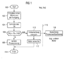
- a Measuring device explained in more detail below is described in a following Method step 104 the temperature coefficient TK (T1) at a reference temperature T1 automatically according to the procedure determined according to standard EIA / JESD33-A.
- a step 106 the actual temperature coefficient TK (T1) with the lower setpoint TKU and the upper one Setpoint TKO compared. Is the actual temperature coefficient TK (T1) between the lower setpoint TKU and the upper setpoint TKO, it is assumed that the microstructure the test track and thus also the microstructure of the The same processes produced interconnects of the circuit arrangement corresponds to a predetermined target microstructure.
- a method step follows immediately after method step 106 108, in which the wafer of further processing is fed. The process control for the production of the Lanes are not changed.
- Method step 106 If, on the other hand, it is determined in method step 106 that the Actual temperature coefficient TK not between the lower setpoint TKU and the upper setpoint TKO, follows after Method step 106 immediately involves a method step 110.
- method step 110 an error message is generated that on the deviation of the actual temperature coefficient TK (T1) from Indicates target range.
- the wafer is no longer considered marked for processing and taken from production. Alternatively, the wafer is marked as being of lower quality and further processed.
- method step 108 and method step 112 follows a method step 114, in which the method regarding of the wafer under consideration is ended.
- a dashed line 116 illustrates the separation of the Effects regarding the tested wafer and regarding other wafer.
- FIG. 2 shows the dependency in a coordinate system 150 the resistance R of a copper interconnect from the temperature T.
- the coordinate system 150 has an x-axis 152 for display the values of the temperature T in ° C (degrees Celsius) and a y-axis 154 to represent the values of the resistance R. Die Relationship between the temperature T and the resistance R. linear and is represented by a straight line 156, the one Has an increase of about 45 ° and the y-axis 154 above the Coordinate origin intersects at a resistance value R0.
- a temperature T1 which in the exemplary embodiment is the reference temperature for the comparison of temperature coefficients serves, corresponds e.g. an ambient temperature of 20 ° C.
- a temperature T2 has e.g. the value 80 ° C and becomes like that Temperature T1 for determining the temperature coefficient TK (T1) used.
- the ratio ⁇ R / ⁇ T indicates the slope A of the straight line 156 or the tangent of an angle W1 between the straight line 156 and the x-axis 152.
- the temperature coefficient TK (T1) easily determined by that initially the resistance R (T1) at the temperature T1 is measured. Subsequently, the one carrying the guideway Wafers heated to the temperature T2 of 80 ° C. At this Then the temperature R (T2) is measured. Subsequently becomes the temperature coefficient according to the formula given above TK (T1) calculated.
- ⁇ R is then determined from the mean values. Also averaging over several recorded temperatures T1 and T2 are carried out when the measuring temperature fluctuates.
- Steps 1 to 4 are the same as in paragraphs 4.3.1.1 to 4.3.1.4 specified process steps of the EIA / JESD33-A standard from EIA (Electronic Industries Association / Solid State Technology Association, formerly known as a Joint Electron Device Engineering Council) "standard method for measuring and using the temperature coefficient of resistance to determine the temperature of a metallization line ", October 1995.
- EIA Electronic Industries Association / Solid State Technology Association, formerly known as a Joint Electron Device Engineering Council
- the trace 200 was created using a dual damascene method introduced into the insulating layer 208.
- a layer of liner 214 for example from titanium nitride, tantalum nitride or tantalum, separates the interconnect 200 from the insulating layer 208th
- grain boundaries 220, 222 and 224 are two crystallites 226 and 228 or grains of the interconnect 200 are shown.
- the crystallite bounded by grain boundaries 220 and 222 226 has in the tangential direction to the surface of the semiconductor substrate a width B1 of, for example, 350 nm, which is approximately the Corresponds to the width of the interconnect 200.
- the one through the grain boundaries 222 and 224 limited crystallite 228 has a width B2 that is slightly smaller than the width B1.
- a lattice defect GF in crystallite 226 is represented by a cross.
- the temperature coefficient a short track and a long track determined. From the comparison of the temperature coefficients for Both interconnects are used to draw conclusions about the density of lattice defects GF or pulled by other defects.
- every temperature is the reference temperature Tref suitable, e.g. also a temperature of 0 ° C.
- the reference temperature is in place of the temperature T1 Use Tref.
- the sizes R (T1) and TK (T1) occur.
Landscapes
- Testing Or Measuring Of Semiconductors Or The Like (AREA)
Abstract
Description
- die Rasterelektronenmikroskopie,
- die Transmissionselektronenmikroskopie,
- die Analyse mit Hilfe eines fokussierten Ionenstrahls,
- das sogenannte automatische Kristall-Orientierungs-Mapping, oder
- eine Texturanalyse durch Röntgenbeugung.
- ein Prozessparameter mit einem maßgeblichen Einfluss auf die Größe von Kristalliten bzw. Körnern in der Metallisierungsanordnung, z.B. die Temperatur bei einem Tempervorgang, die Temperatur beim Aufbringen der Metallisierung, oder auch die ursprüngliche Dicke der Metallisierungsschicht nach dem Aufbringen,
- ein Prozessparameter, der die Form der Kristallite maßgeblich beeinflusst,
- ein Prozessparameter, der die Art oder den Anteil der vorhandenen Phasen maßgeblich beeinflusst,
- ein Prozessparameter, der die Substruktur der Kristallite maßgeblich beeinflusst, insbesondere hinsichtlich von Gitterfehlern, Leerstellen, Versetzungen, Stapelfehler oder Zwillingskristalliten, wobei beispielsweise eine Plasmabehandlung bzw. eine Ionenbestrahlung oder eine mechanische Krafteinwirkung einen maßgeblichen Einfluss haben, oder
- ein Prozessparameter, der die gegenseitige Anordnung und Ausrichtung der Kristallite und Phasenanteile maßgeblich beeinflusst.
- Figur 1
- Verfahrensschritte zur Überwachung der Herstellung von integrierten Schaltkreisen,
- Figur 2
- die Abhängigkeit des Widerstandes einer Leitbahn von der Temperatur, und
- Figur 3
- die Mikrostruktur einer Leitbahn.
- eine elektrische Isolierschicht 204, beispielsweise aus Siliziumdioxid oder einem sogenannten low-k-Material (k bezeichnet die Dielektrizitätskonstante), eine Zwischenschicht 206, z.B. aus Siliziumnitrid oder Siliziumcarbid,
- eine Isolierschicht 208, z.B. aus Siliziumdioxid, eine Zwischenschicht 210, z.B. aus Siliziumnitrid oder Siliziumcarbid, und eine obere Isolierschicht 212, z.B. aus Siliziumdioxid.
- eine Haltevorrichtung zum Halten des Wafers, z.B. einen sogenannten Wafer-Chuck,
- Anschlusselektroden zum Anschließen der Konstantstromquelle an die Anschlüsse A1 und A2, z.B. eine sogenannte Nadelkarte,
- eine Heizeinrichtung, z.B. ein Heizbarer Wafer-Chuck zur externen Waferheizung oder ein in den Wafer integrierter Heizer, der z.B. Polysiliziumstreifen enthält und dessen Temperatur z.B. über eine in den Wafer integrierte Diode überwacht wird,
- und eine Steuereinheit, welche die an Hand der Figur 1 erläuterten Verfahrensschritte 104, 106 und 110 automatisch ausführt. Die Steuereinrichtung ist entweder eine elektronische Schaltung ohne Prozessor oder eine elektronische Datenverarbeitungsanlage, die einen Prozessor enthält, der Befehle eines Programms ausführt.
Claims (15)
- Verfahren zum Überwachen der Herstellung einer Metallisierungsanordnung (200), insbesondere einer integrierten Metallisierungsanordnung (200),
bei dem ein Sollwert (TKU) oder ein Sollbereich (TKU, TKO) für eine physikalische Größe (TK) vorgegeben wird, die ein Maß für die Temperaturabhängigkeit des elektrischen Widerstandes (R) einer herzustellenden Metallisierungsanordnung (200) ist (100),
bei dem die Metallisierungsanordnung (200) hergestellt wird (102),
bei dem für die Metallisierungsanordnung (200) ein Istwert (TK(T1)) für die physikalische Größe (TK) ermittelt wird (104),
und bei dem aufgrund eines Vergleichs von Istwert (TK(T1)) und Sollwert (TKU) oder Sollbereich (TKU, TKO) die Herstellung der Metallisierungsanordnung (202) oder die Herstellung mindestens einer gleichzeitig mit der Metallisierungsanordnung (202) hergestellten anderen Metallisierungsanordnung oder ein Herstellungsprozess zum Herstellen von Metallisierungsanordnungen (202) überwacht wird (106). - Verfahren nach Anspruch 1, dadurch gekennzeichnet, dass die Metallisierungsanordnung (200) eine in einem Dielektrikum (208) einer integrierten Schaltungsanordnung (202) geführte Leitbahn ist,
und/oder dass die Metallisierungsanordnung in mindestens einer Richtung eine Abmessung kleiner hundert Mikrometer oder kleiner als ein Mikrometer hat,
und/oder dass die Metallisierungsanordnung (200) aus Kupfer oder einer Kupferlegierung besteht, die mindestens fünfzig Prozent Kupfer enthält. - Verfahren nach Anspruch 1 oder 2, dadurch gekennzeichnet, dass zur Bestimmung des Sollwertes (TKU) oder des Sollbereiches (TKU, TKO) mindestens ein Istwert für die physikalische Größe (TK) für mindestens eine Metallisierungsanordnung ermittelt wird, die die gleiche äußere Struktur wie die herzustellende Metallisierungsanordnung (200) hat und/oder deren innere Struktur einer Sollstruktur entspricht.
- Verfahren nach einem der vorhergehenden Ansprüche, dadurch gekennzeichnet, dass die physikalische Größe der Temperaturkoeffizient (TK) bei einer Referenztemperatur (T1) ist.
- Verfahren nach einem der vorhergehenden Ansprüche, dadurch gekennzeichnet, dass zum Ermitteln des Istwertes (TK(T1)) der Widerstand (R) der Metallisierungsanordnung (200) bei mindestens zwei verschiedenen Temperaturen (T1, T2) ermittelt und/oder gemessen wird,
und/oder dass zum Ermitteln des Istwertes (TK(T1)) das in dem Standard EIA/JESD33-A oder einem auf diesen Standard aufbauenden Standard angegebene Verfahren zum Ermitteln des Temperaturkoeffizienten (TCR) bei einer Referenztemperatur (Tref) ausgeführt wird. - Verfahren nach einem der vorhergehenden Ansprüche, dadurch gekennzeichnet, dass bei einer Abweichung des Istwertes (TK(T1)) vom Sollwert (TKU) oder vom Sollbereich (TKU, TKO) zuerst die Einhaltung eines Prozessparameters geprüft wird, der einen maßgeblichen Einfluss auf die Größe von Kristalliten (226, 228) in der Metallisierungsanordnung (200) hat, vorzugsweise die Temperatur eines Temperofens oder einer Sputteranlage,
und/oder die Einhaltung eines Parameters, der die Form der Kristallite (226, 228) maßgeblich beeinflusst,
und/oder die Einhaltung eines Parameters, der Art und/oder den Anteil der in der Metallisierungsanordnung (200) vorhandenen Phasen maßgeblich beeinflusst,
und/oder die Einhaltung eines Parameters, der die Substruktur der Kristallite (226, 228) maßgeblich beeinflusst, insbesondere hinsichtlich von Gitterfehlern (GF) und/oder Leerstellen und/oder Versetzungen und/oder Stapelfehlern und/oder Zwillingskristalliten,
und/oder die Einhaltung eines Parameters, der die gegenseitige Anordnung und Ausrichtung der Kristallite (226, 228) und/oder der Phasenanteile zueinander maßgeblich beeinflusst. - Verfahren nach einem der vorhergehenden Ansprüche, dadurch gekennzeichnet, dass bei einer Abweichung des Istwertes (TK(T1)) vom Sollwert (TKU) oder vom Sollbereich (TKU, TKO) automatisch eine Fehlermeldung in einer Datei vermerkt oder auf einer Anzeigeeinheit ausgegeben wird (110).
- Verfahren nach einem der vorhergehenden Ansprüche, dadurch gekennzeichnet, dass es in regelmäßigen Abständen bezogen auf die Anzahl prozessierter Metallisierungsanordnungen oder die Prozesszeit des gleichen Produktionsprozesses durchgeführt wird.
- Verfahren zum Bewerten der Qualität einer Metallisierungsanordnung (200), insbesondere einer integrierten Metallisierungsanordnung,
bei dem ein Sollwert (TKU) oder ein Sollbereich (TKU, TKO) für eine physikalische Größe (TK) vorgegeben wird, die ein Maß für die Temperaturabhängigkeit des elektrischen Widerstandes (R) einer herzustellenden Metallisierungsanordnung (200) ist (100),
bei dem die Metallisierungsanordnung (200) hergestellt wird (102),
bei dem für die Metallisierungsanordnung (200) ein Istwert (TK (T1)) für die physikalische Größe (TK) ermittelt wird (104),
und bei dem aufgrund eines Vergleichs von Istwert (TK(T1)) und Sollwert (TKU) oder Sollbereich (TKU, TKO) die Qualität der Metallisierungsanordnung (200) bewertet wird. - Verfahren nach Anspruch 9, dadurch gekennzeichnet, dass abhängig von der Qualität ein Verfahrensschritt zur weiteren Bearbeitung der Metallisierungsanordnung (200) oder zur weiteren Bearbeitung einer integrierten Schaltungsanordnung (202) ausgeführt oder unterlassen wird (108, 112).
- Verfahren nach Anspruch 9 oder 10, gekennzeichnet durch mindestens einen Verfahrensschritt nach einem der Ansprüche 1 bis 8.
- Verfahren nach einem der Ansprüche 9 bis 11, dadurch gekennzeichnet, dass es zum Vergleichen von neuen Abscheideverfahren und/oder Temperverfahren bezüglich älterer Verfahren oder bezüglich anderer neuer Verfahren verwendet wird.
- Erfassungsvorrichtung für die Überwachung der Herstellung einer Metallisierungsanordnung,
mit einer Halteeinrichtung für eine Metallisierungsanordnung oder für ein die Metallisierungsanordnung (200) tragendes Substrat,
mit Anschlusselektroden zum Einspeisen eines Messstroms in oder zum Anlegen einer Messspannung an die Metallisierungsanordnung (200),
mit einer Erfassungseinrichtung zum Erfassen einer Spannung an oder eines Stromes durch die Metallisierungsanordnung (200),
mit einer Heizeinrichtung,
mit einer Temperatureinstelleinrichtung oder Temperaturregeleinrichtung,
und mit einer Steuereinheit,
wobei die Steuereinheit nach dem Aufnehmen der Metallisierungsanordnung (200) in die Halteeinrichtung automatisch eine physikalische Größe (TK) ermittelt, die ein Maß für die Temperaturabhängigkeit des elektrischen Widerstandes (R) der Metallisierungsanordnung (200) ist. - Erfassungsvorrichtung nach Anspruch 13, gekennzeichnet durch eine Speichereinheit, die einen vorgegebenen Sollwert (TKU) oder Werte (TKU, TKO) eines Sollbereiches speichert,
durch eine Vergleichseinheit, die einen Istwert (TK(T1)) der physikalischen Größe mit dem Sollwert (TKU) oder mit den Werten (TKU, TKO) des Sollbereiches vergleicht,
und durch eine Fehlermeldungseinheit, die abhängig vom Vergleichsergebnis automatisch eine Fehlermeldung erzeugt. - Erfassungsvorrichtung nach Anspruch 13 oder 14, gekennzeichnet durch Einheiten, bei deren Betrieb mindestens ein Verfahrensschritt eines Verfahrens nach einem der Ansprüche 1 bis 12 ausgeführt wird.
Applications Claiming Priority (2)
| Application Number | Priority Date | Filing Date | Title |
|---|---|---|---|
| DE10227829A DE10227829A1 (de) | 2002-06-21 | 2002-06-21 | Verfahren zum Überwachen der Herstellung und zum Bewerten der Qualität einer Metallisierungsanordnung sowie zugehörige Erfassungsvorrichtung |
| DE10227829 | 2002-06-21 |
Publications (1)
| Publication Number | Publication Date |
|---|---|
| EP1376680A1 true EP1376680A1 (de) | 2004-01-02 |
Family
ID=29716587
Family Applications (1)
| Application Number | Title | Priority Date | Filing Date |
|---|---|---|---|
| EP03012799A Ceased EP1376680A1 (de) | 2002-06-21 | 2003-06-05 | Verfahren zum Überwachen der Herstellung und zum Bewerten der Qualität einer Metallisierungsanordnung sowie zugehörige Erfassungsvorrichtung |
Country Status (2)
| Country | Link |
|---|---|
| EP (1) | EP1376680A1 (de) |
| DE (1) | DE10227829A1 (de) |
Cited By (3)
| Publication number | Priority date | Publication date | Assignee | Title |
|---|---|---|---|---|
| US5902110A (en) * | 1995-12-18 | 1999-05-11 | The Block Drug Company | Bone regeneration |
| DE102007020252A1 (de) * | 2007-04-30 | 2008-11-06 | Advanced Micro Devices, Inc., Sunnyvale | Technik zur Herstellung von Metallleitungen in einem Halbleiter durch Anpassen der Temperaturabhängigkeit des Leitungswiderstands |
| US7500208B2 (en) | 2004-09-17 | 2009-03-03 | International Business Machines Corporation | Non-destructive evaluation of microstructure and interface roughness of electrically conducting lines in semiconductor integrated circuits in deep sub-micron regime |
Citations (5)
| Publication number | Priority date | Publication date | Assignee | Title |
|---|---|---|---|---|
| US4483629A (en) * | 1983-01-05 | 1984-11-20 | Syracuse University | Dynamic testing of electrical conductors |
| EP0253746A1 (de) * | 1986-07-11 | 1988-01-20 | Syracuse University | Verfahren und Vorrichtung zum dynamischen Testen eines Dünnfilm-Leiters |
| EP0448273A1 (de) * | 1990-03-21 | 1991-09-25 | AT&T Corp. | Elektromigrationsüberwachungseinrichtung für integrierte Schaltungen |
| US5260668A (en) * | 1992-06-11 | 1993-11-09 | Prometrix Corporation | Semiconductor surface resistivity probe with semiconductor temperature control |
| JPH06342027A (ja) | 1993-06-01 | 1994-12-13 | Nippondenso Co Ltd | 配線の評価方法及び評価装置 |
Family Cites Families (1)
| Publication number | Priority date | Publication date | Assignee | Title |
|---|---|---|---|---|
| CA2406371A1 (en) * | 2000-04-17 | 2001-10-25 | Martin Gall | Electromigration early failure distribution in submicron interconnects |
-
2002
- 2002-06-21 DE DE10227829A patent/DE10227829A1/de not_active Ceased
-
2003
- 2003-06-05 EP EP03012799A patent/EP1376680A1/de not_active Ceased
Patent Citations (5)
| Publication number | Priority date | Publication date | Assignee | Title |
|---|---|---|---|---|
| US4483629A (en) * | 1983-01-05 | 1984-11-20 | Syracuse University | Dynamic testing of electrical conductors |
| EP0253746A1 (de) * | 1986-07-11 | 1988-01-20 | Syracuse University | Verfahren und Vorrichtung zum dynamischen Testen eines Dünnfilm-Leiters |
| EP0448273A1 (de) * | 1990-03-21 | 1991-09-25 | AT&T Corp. | Elektromigrationsüberwachungseinrichtung für integrierte Schaltungen |
| US5260668A (en) * | 1992-06-11 | 1993-11-09 | Prometrix Corporation | Semiconductor surface resistivity probe with semiconductor temperature control |
| JPH06342027A (ja) | 1993-06-01 | 1994-12-13 | Nippondenso Co Ltd | 配線の評価方法及び評価装置 |
Non-Patent Citations (3)
| Title |
|---|
| GONELLA R; TORRES J; MOTTE P; VAN DER VEGT E; GILET J M: "Impact of process steps on electrical and electromigration performances of copper interconnects in damascene architecture", MICROELECTRONICS RELIABILITY, vol. 40, no. 8-10, August 2000 (2000-08-01) - October 2000 (2000-10-01), Elsevier, pages 1329 - 1334, XP009120651, ISSN: 0026-2714 * |
| PATENT ABSTRACTS OF JAPAN vol. 1995, no. 03 28 April 1995 (1995-04-28) * |
| R. GONELLA ET AL.: "Impact of process steps on electrical and electromigration performances of copper interconnects in damascene architecture", MICROELECTRONICS RELIABILITY, vol. 40, 2000, pages 1329 - 1334, XP009120651, DOI: doi:10.1016/S0026-2714(00)00121-9 |
Cited By (4)
| Publication number | Priority date | Publication date | Assignee | Title |
|---|---|---|---|---|
| US5902110A (en) * | 1995-12-18 | 1999-05-11 | The Block Drug Company | Bone regeneration |
| US7500208B2 (en) | 2004-09-17 | 2009-03-03 | International Business Machines Corporation | Non-destructive evaluation of microstructure and interface roughness of electrically conducting lines in semiconductor integrated circuits in deep sub-micron regime |
| DE102007020252A1 (de) * | 2007-04-30 | 2008-11-06 | Advanced Micro Devices, Inc., Sunnyvale | Technik zur Herstellung von Metallleitungen in einem Halbleiter durch Anpassen der Temperaturabhängigkeit des Leitungswiderstands |
| US8058731B2 (en) | 2007-04-30 | 2011-11-15 | Advanced Micro Devices, Inc | Technique for forming metal lines in a semiconductor by adapting the temperature dependence of the line resistance |
Also Published As
| Publication number | Publication date |
|---|---|
| DE10227829A1 (de) | 2004-01-15 |
Similar Documents
| Publication | Publication Date | Title |
|---|---|---|
| DE2554536C2 (de) | Verfahren zum Bestimmen der Breite und/oder des Schichtwiderstandes von flächenhaften Leiterzügen integrierter Schaltungen | |
| DE112004001259B4 (de) | Verfahren und System zum Ausführen einer Messverteilung auf der Grundlage einer Fehlererkennung und computerlesbares Speichermedium | |
| DE10228720A1 (de) | Verbesserte Impuls-Spannungsdurchbruch(VBD-)Technik zur Inline-Kontrolle der Gateoxidzuverlässigkeit | |
| DE10393903T5 (de) | Dynamische adaptive Abtastrate für Modellvorhersage | |
| DE10103061B4 (de) | Verfahren zur Inspektion der Tiefe einer Öffnung in einer dielektrischen Materialschicht | |
| WO2016180756A1 (de) | Kontaktviakette als korrosionsdetektor | |
| DE102015118309A1 (de) | Verfahren zum bearbeiten eines substrats und verfahren zum überprüfen eines prozesses für integrierte schaltungen | |
| DE102005041283B4 (de) | Verfahren und Halbleiterstruktur zur Überwachung der Herstellung von Verbindungsstrukturen und Kontakten in einem Halbleiterbauelement | |
| WO2002067318A2 (de) | Elektromigrations-teststruktur zur erfassung der zuverlässigkeit von verdrahtungen | |
| DE10240115B4 (de) | Verfahren und System zum Handhaben von Substraten in einer Produktionslinie mit einer Cluster-Anlage und einer Messanlage | |
| DE102007020257A1 (de) | Vereinheitlichte Teststruktur für belastungsabhängige Materialwanderungsprüfungen | |
| EP1376680A1 (de) | Verfahren zum Überwachen der Herstellung und zum Bewerten der Qualität einer Metallisierungsanordnung sowie zugehörige Erfassungsvorrichtung | |
| DE102011076109A1 (de) | Halbleitertestverfahren und -gerät und Halbleitervorrichtung | |
| DE69305450T2 (de) | Verfahren zur Prüfung des Schichtwiderstandes einer Diffusionsschicht | |
| DE10252605A1 (de) | Verfahren, Vorrichtung, computerlesbarer Speicher und Computerprogramm-Element zum rechnergestützten Überwachen und Regeln eines Herstellungsprozesses | |
| WO2020156899A1 (de) | Verfahren und system zur thermischen anbindung einer wärmequelle eines batteriesystems an eine wärmesenke eines batteriesystems | |
| DE102008022201B4 (de) | Vorrichtung und Verfahren zum Messen einer lokalen Oberflächentemperatur eines Halbleiterbauelements | |
| DE102006062034B4 (de) | Teststruktur mit erhöhter Robustheit im Hinblick auf Barrieredefekte in Kontaktlochöffnungen beim Abschätzen von Elektromigrationseffekten sowie dazugehöriges Herstellungsverfahren | |
| DE102006039546A1 (de) | Verfahren und Mess-Schaltung zum Bestimmen der Zuverlässigkeit eines integrierten Schaltkreises | |
| WO2008046925A1 (de) | Teststruktur für hoch beschleunigte elektromigrationstests für dicke metallisierungssysteme von festkörperschaltkreisen | |
| DE69104248T2 (de) | Elektromigrationsüberwachungseinrichtung für integrierte Schaltungen. | |
| EP3295190B1 (de) | Anordnung von leitbahnen, vorrichtung und verfahren zur fehlerbestimmung einer halbleiterschaltung | |
| EP1723402B1 (de) | Prüfung der dichtigkeit von scheibenbondverbindungen und teststruktur zur durchführung des verfahrens | |
| DE10213609B4 (de) | Elektrisches Bauelement mit einer Kontaktierungsfläche und Verfahren zum Ausbilden einer Kontaktierungsfläche auf einem Halbleitermaterial | |
| EP1420314A2 (de) | Verfahren, Vorrichtung, computerlesbares Speichermedium und Computerprogramm-Element zum Überwachen eines Herstellungsprozesses einer Mehrzahl von physikalischen Objekten |
Legal Events
| Date | Code | Title | Description |
|---|---|---|---|
| PUAI | Public reference made under article 153(3) epc to a published international application that has entered the european phase |
Free format text: ORIGINAL CODE: 0009012 |
|
| AK | Designated contracting states |
Kind code of ref document: A1 Designated state(s): AT BE BG CH CY CZ DE DK EE ES FI FR GB GR HU IE IT LI LU MC NL PT RO SE SI SK TR |
|
| AX | Request for extension of the european patent |
Extension state: AL LT LV MK |
|
| 17P | Request for examination filed |
Effective date: 20040126 |
|
| 17Q | First examination report despatched |
Effective date: 20040224 |
|
| AKX | Designation fees paid |
Designated state(s): DE FR IT |
|
| 17Q | First examination report despatched |
Effective date: 20040224 |
|
| APBK | Appeal reference recorded |
Free format text: ORIGINAL CODE: EPIDOSNREFNE |
|
| APBN | Date of receipt of notice of appeal recorded |
Free format text: ORIGINAL CODE: EPIDOSNNOA2E |
|
| RAP1 | Party data changed (applicant data changed or rights of an application transferred) |
Owner name: INFINEON TECHNOLOGIES AG |
|
| APBR | Date of receipt of statement of grounds of appeal recorded |
Free format text: ORIGINAL CODE: EPIDOSNNOA3E |
|
| APAF | Appeal reference modified |
Free format text: ORIGINAL CODE: EPIDOSCREFNE |
|
| APBT | Appeal procedure closed |
Free format text: ORIGINAL CODE: EPIDOSNNOA9E |
|
| STAA | Information on the status of an ep patent application or granted ep patent |
Free format text: STATUS: THE APPLICATION HAS BEEN REFUSED |
|
| 18R | Application refused |
Effective date: 20140605 |