EP1376143A2 - Apparatus for displaying the distribution of an electric property of an electronic appliance - Google Patents
Apparatus for displaying the distribution of an electric property of an electronic appliance Download PDFInfo
- Publication number
- EP1376143A2 EP1376143A2 EP03000808A EP03000808A EP1376143A2 EP 1376143 A2 EP1376143 A2 EP 1376143A2 EP 03000808 A EP03000808 A EP 03000808A EP 03000808 A EP03000808 A EP 03000808A EP 1376143 A2 EP1376143 A2 EP 1376143A2
- Authority
- EP
- European Patent Office
- Prior art keywords
- distribution
- electronic appliance
- electric
- displayed
- displaying
- Prior art date
- Legal status (The legal status is an assumption and is not a legal conclusion. Google has not performed a legal analysis and makes no representation as to the accuracy of the status listed.)
- Withdrawn
Links
Images







Classifications
-
- G—PHYSICS
- G01—MEASURING; TESTING
- G01R—MEASURING ELECTRIC VARIABLES; MEASURING MAGNETIC VARIABLES
- G01R31/00—Arrangements for testing electric properties; Arrangements for locating electric faults; Arrangements for electrical testing characterised by what is being tested not provided for elsewhere
- G01R31/001—Measuring interference from external sources to, or emission from, the device under test, e.g. EMC, EMI, EMP or ESD testing
-
- G—PHYSICS
- G01—MEASURING; TESTING
- G01R—MEASURING ELECTRIC VARIABLES; MEASURING MAGNETIC VARIABLES
- G01R29/00—Arrangements for measuring or indicating electric quantities not covered by groups G01R19/00 - G01R27/00
- G01R29/08—Measuring electromagnetic field characteristics
- G01R29/0864—Measuring electromagnetic field characteristics characterised by constructional or functional features
- G01R29/0892—Details related to signal analysis or treatment; presenting results, e.g. displays; measuring specific signal features other than field strength, e.g. polarisation, field modes, phase, envelope, maximum value
Definitions
- the present invention relates to an electronic appliance displaying apparatus for identifying and displaying a generating source of electromagnetic-wave noises radiated from an electronic appliance, an electronic appliance designed to reduce the electromagnetic-wave noises radiated therefrom, and a manufacturing method thereof.
Landscapes
- Physics & Mathematics (AREA)
- Electromagnetism (AREA)
- General Physics & Mathematics (AREA)
- Tests Of Electronic Circuits (AREA)
- Controls And Circuits For Display Device (AREA)
Abstract
Description
wherein, at least at one of the above-described steps, at least one of the electric-current distribution, the electric-voltage distribution, the electric-power distribution, and the impedance distribution is derived from the above-described magnetic-field distribution, and the derived distribution is superposition-displayed on a screen showing an image of the electronic appliance, CAD data thereon, layout data thereon, or a circuit diagram thereof.
Claims (11)
- An electronic appliance displaying apparatus for displaying at least one of electric-current distribution (203, 203, 203), electric-voltage distribution, electric-power distribution, and impedance distribution that are derived from magnetic-field distribution existing in vicinities of an electronic appliance, wherein, said derived distribution is superposition-displayed (201, 601, 1201) on an image of said electronic appliance, CAD data thereon, layout data thereon, or a circuit diagram thereof (202, 502, 1102).
- The electronic appliance displaying apparatus as claimed in claim 1, wherein, in performing the superposition display (201, 601, 1201), said target to be measured is displayed on a black-and-white display or on its gray-scale display.
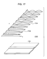
- The electronic appliance displaying apparatus as claimed in claim 1, wherein said distribution is displayed on a view (1702) implemented in correspondence with frequency variation.
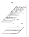
- The electronic appliance displaying apparatus as claimed in claim 1, wherein said distribution is displayed on a view (1801) implemented in correspondence with time variation.
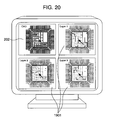
- The electronic appliance displaying apparatus as claimed in claim 1, wherein said distribution is displayed on a view (1901) varied for each cross-section of said electronic appliance.
- An electronic appliance displaying apparatus for displaying magnetic-field distribution existing in vicinities of an electronic appliance, wherein said magnetic-field distribution, and an image of said electronic appliance, CAD data thereon, layout data thereon, or a circuit diagram thereof (202, 502, 1102) are displayed on plural views (301, 801, 1401).
- The electronic appliance displaying apparatus as claimed in claim 6, wherein pointers for indicating an identical coordinate are displayed on said view displaying said magnetic-field distribution, and on said view displaying said image of said electronic appliance, said CAD data thereon, said layout data thereon, or the circuit diagram thereof (202, 502, 1102).
- The electronic appliance displaying apparatus as claimed in claim 6, wherein said electronic appliance displaying apparatus derives from said magnetic-field distribution, and displays at least one of electric-current distribution (203, 203, 203), electric-voltage distribution, electric-power distribution, and impedance distribution.
- The electronic appliance displaying apparatus as claimed in claim 8, wherein pointers for indicating an identical coordinate are displayed on said view displaying said derived distribution, and on said view displaying said image of said electronic appliance, said CAD data thereon, said layout data thereon, or said circuit diagram thereof (202, 502, 1102).
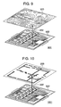
- An electronic appliance displaying apparatus for displaying magnetic-field distribution existing in vicinities of an electronic appliance, wherein said magnetic-field distribution is separation-displayed (401, 1001, 1601) for each layer of said electronic appliance.
- The electronic appliance displaying apparatus as claimed in claim 10, wherein said electronic appliance displaying apparatus derives from said magnetic-field distribution on each layer basis, and displays at least one of electric-current distribution (203), electric-voltage distribution, electric-power distribution, and impedance distribution.
Applications Claiming Priority (2)
| Application Number | Priority Date | Filing Date | Title |
|---|---|---|---|
| JP2002176540 | 2002-06-18 | ||
| JP2002176540A JP2004020403A (en) | 2002-06-18 | 2002-06-18 | Electronic device display device, electronic device, and manufacturing method thereof |
Publications (2)
| Publication Number | Publication Date |
|---|---|
| EP1376143A2 true EP1376143A2 (en) | 2004-01-02 |
| EP1376143A3 EP1376143A3 (en) | 2004-04-07 |
Family
ID=29717456
Family Applications (1)
| Application Number | Title | Priority Date | Filing Date |
|---|---|---|---|
| EP03000808A Withdrawn EP1376143A3 (en) | 2002-06-18 | 2003-01-14 | Apparatus for displaying the distribution of an electric property of an electronic appliance |
Country Status (4)
| Country | Link |
|---|---|
| US (1) | US20030231145A1 (en) |
| EP (1) | EP1376143A3 (en) |
| JP (1) | JP2004020403A (en) |
| CA (1) | CA2416350A1 (en) |
Cited By (3)
| Publication number | Priority date | Publication date | Assignee | Title |
|---|---|---|---|---|
| EP1837666A4 (en) * | 2005-01-11 | 2011-08-24 | Taiyo Yuden Kk | Electromagnetic field distribution measuring method and apparatus thereof, computer program and information recording medium |
| JP2014240775A (en) * | 2013-06-11 | 2014-12-25 | 三菱電機株式会社 | Electromagnetic noise detection device |
| EP4130762A4 (en) * | 2020-03-27 | 2023-05-10 | Kabushiki Kaisha Zuken | DESIGN AID DEVICE, DESIGN AID METHOD AND PROGRAM |
Families Citing this family (5)
| Publication number | Priority date | Publication date | Assignee | Title |
|---|---|---|---|---|
| JP5611875B2 (en) * | 2011-03-18 | 2014-10-22 | 株式会社Pfu | Information display device, information display method, and program |
| WO2014065032A1 (en) * | 2012-10-24 | 2014-05-01 | 日本電気株式会社 | Electromagnetic field feature classification and presentation device |
| JP6618694B2 (en) * | 2015-03-23 | 2019-12-11 | 国立研究開発法人情報通信研究機構 | Electric field imaging method |
| WO2021024713A1 (en) * | 2019-08-02 | 2021-02-11 | パナソニックIpマネジメント株式会社 | Electromagnetic wave visualization device |
| CN112130003B (en) * | 2020-09-03 | 2021-11-09 | 南京理工大学 | Device and method for removing electromagnetic interference signals in same frequency band |
Family Cites Families (17)
| Publication number | Priority date | Publication date | Assignee | Title |
|---|---|---|---|---|
| JP3428232B2 (en) * | 1995-06-16 | 2003-07-22 | 富士通株式会社 | Electromagnetic field strength calculator |
| US5986673A (en) * | 1997-10-17 | 1999-11-16 | Martz; David R. | Method for relational ordering and displaying multidimensional data |
| JPH11166963A (en) * | 1997-12-04 | 1999-06-22 | Kyodo Kumiai Joint Labo Sendai | Magnetic field direction detection method |
| JP3189801B2 (en) * | 1998-08-28 | 2001-07-16 | 日本電気株式会社 | Semiconductor evaluation device, magnetic field detector used therefor, manufacturing method thereof, and storage medium storing semiconductor evaluation program |
| JP3394202B2 (en) * | 1999-01-13 | 2003-04-07 | 太陽誘電株式会社 | Method and apparatus for measuring electromagnetic field intensity and method and apparatus for measuring current-voltage distribution |
| US6486898B1 (en) * | 1999-03-31 | 2002-11-26 | Koninklijke Philips Electronics N.V. | Device and method for a lattice display |
| JP2000304790A (en) * | 1999-04-23 | 2000-11-02 | Hitachi Ltd | Apparatus for locating electromagnetic wave source, its method and its analysis method |
| JP3454235B2 (en) * | 1999-10-06 | 2003-10-06 | 株式会社日立製作所 | Biomagnetic field measurement device |
| JP2001156133A (en) * | 1999-11-25 | 2001-06-08 | Nec Corp | Positioning method for lsi potential distribution image |
| WO2001061456A2 (en) * | 2000-02-14 | 2001-08-23 | Geophoenix, Inc. | Methods and apparatus for viewing information in virtual space |
| US20020089541A1 (en) * | 2000-02-14 | 2002-07-11 | Julian Orbanes | System for graphically interconnecting operators |
| US20020089550A1 (en) * | 2000-02-14 | 2002-07-11 | Julian Orbanes | Method and apparatus for organizing hierarchical screens in virtual space |
| JP2001305169A (en) * | 2000-04-18 | 2001-10-31 | Ryowa Denshi Kk | Display device |
| US20020033706A1 (en) * | 2000-08-03 | 2002-03-21 | Mehyar Khazei | System method, and apparatus for field scanning |
| US7034831B2 (en) * | 2001-02-05 | 2006-04-25 | National Instruments Corporation | System and method for generating a low discrepancy curve in a region |
| US7043702B2 (en) * | 2001-03-15 | 2006-05-09 | Xerox Corporation | Method for visualizing user path through a web site and a path's associated information scent |
| US7114132B2 (en) * | 2001-04-20 | 2006-09-26 | Nec Corporation | Device, system, server, client, and method for supporting component layout design on circuit board, and program for implementing the device |
-
2002
- 2002-06-18 JP JP2002176540A patent/JP2004020403A/en active Pending
-
2003
- 2003-01-14 CA CA002416350A patent/CA2416350A1/en not_active Abandoned
- 2003-01-14 EP EP03000808A patent/EP1376143A3/en not_active Withdrawn
- 2003-01-17 US US10/346,912 patent/US20030231145A1/en not_active Abandoned
Cited By (4)
| Publication number | Priority date | Publication date | Assignee | Title |
|---|---|---|---|---|
| EP1837666A4 (en) * | 2005-01-11 | 2011-08-24 | Taiyo Yuden Kk | Electromagnetic field distribution measuring method and apparatus thereof, computer program and information recording medium |
| JP2014240775A (en) * | 2013-06-11 | 2014-12-25 | 三菱電機株式会社 | Electromagnetic noise detection device |
| EP4130762A4 (en) * | 2020-03-27 | 2023-05-10 | Kabushiki Kaisha Zuken | DESIGN AID DEVICE, DESIGN AID METHOD AND PROGRAM |
| US12572710B2 (en) | 2020-03-27 | 2026-03-10 | Kabushiki Kaisha Zuken | Support apparatus, design support method, and non-transitory computer readable medium storing a computer program |
Also Published As
| Publication number | Publication date |
|---|---|
| CA2416350A1 (en) | 2003-12-18 |
| EP1376143A3 (en) | 2004-04-07 |
| US20030231145A1 (en) | 2003-12-18 |
| JP2004020403A (en) | 2004-01-22 |
Similar Documents
| Publication | Publication Date | Title |
|---|---|---|
| JP4635544B2 (en) | Electric field distribution measuring method and electric field distribution measuring apparatus | |
| JP3189801B2 (en) | Semiconductor evaluation device, magnetic field detector used therefor, manufacturing method thereof, and storage medium storing semiconductor evaluation program | |
| US8446152B2 (en) | Printed circuit board test assisting apparatus, printed circuit board test assisting method, and computer-readable information recording medium | |
| US6765667B2 (en) | Method for inspection of circuit boards and apparatus for inspection of circuit boards | |
| EP1376143A2 (en) | Apparatus for displaying the distribution of an electric property of an electronic appliance | |
| US6875920B2 (en) | Semiconductor device and design support method of electronic device using the same | |
| US20150234972A1 (en) | Board design method and board design device | |
| JP2004037222A (en) | Teaching method, electronic substrate inspection method, and electronic substrate inspection device | |
| JP4003403B2 (en) | Electromagnetic source search method | |
| Lin et al. | Design and application of a mobile miniature current probe for analysing the cause of EMI noise in IC circuits | |
| JP2002318253A (en) | Noise visualization system and display method thereof | |
| KR20210146505A (en) | Apparatus and method for simulating performance of electro magnetic compatibility of junction block | |
| CN100543752C (en) | Method for checking return path of printed circuit board and pattern design CAD device thereof | |
| EP3046406B1 (en) | Method for generating compensation matrix during substrate inspection | |
| JP2020165713A (en) | Inspection data output device, display system and inspection data output method | |
| US20190286767A1 (en) | Electromagnetic field simulator, method for operating electromagnetic field simulator, and non-transitory computer readable medium | |
| CN114518491B (en) | Electromagnetic environment analysis system, electromagnetic environment analysis method, and storage medium | |
| CN114545108B (en) | Electromagnetic environment analysis system, electromagnetic environment analysis method and storage medium | |
| JP2011008664A (en) | Method and system for determining emc | |
| JP4283647B2 (en) | Layout check system | |
| Rebholz et al. | A fast radiated emission model for arbitrary cable harness configurations based on measurements and simulations | |
| JP2005134169A (en) | Electromagnetic field measuring method, measuring apparatus, and semiconductor device | |
| CN114545096B (en) | Electromagnetic environment analysis system, electromagnetic environment analysis method, and storage medium | |
| JP3885830B2 (en) | Printed circuit board design support apparatus, design support method, and recording medium recording program used in design support apparatus | |
| Funato et al. | Application of a magnetic near-field probe to the differentiation of defective connections |
Legal Events
| Date | Code | Title | Description |
|---|---|---|---|
| PUAI | Public reference made under article 153(3) epc to a published international application that has entered the european phase |
Free format text: ORIGINAL CODE: 0009012 |
|
| AK | Designated contracting states |
Kind code of ref document: A2 Designated state(s): AT BE BG CH CY CZ DE DK EE ES FI FR GB GR HU IE IT LI LU MC NL PT SE SI SK TR |
|
| AX | Request for extension of the european patent |
Extension state: AL LT LV MK RO |
|
| PUAL | Search report despatched |
Free format text: ORIGINAL CODE: 0009013 |
|
| AK | Designated contracting states |
Kind code of ref document: A3 Designated state(s): AT BE BG CH CY CZ DE DK EE ES FI FR GB GR HU IE IT LI LU MC NL PT SE SI SK TR |
|
| AX | Request for extension of the european patent |
Extension state: AL LT LV MK RO |
|
| RIC1 | Information provided on ipc code assigned before grant |
Ipc: 7G 01R 29/08 B Ipc: 7G 01R 33/10 B Ipc: 7G 01R 31/00 A |
|
| 17P | Request for examination filed |
Effective date: 20040421 |
|
| AKX | Designation fees paid |
Designated state(s): DE FR GB |
|
| 17Q | First examination report despatched |
Effective date: 20050103 |
|
| STAA | Information on the status of an ep patent application or granted ep patent |
Free format text: STATUS: THE APPLICATION IS DEEMED TO BE WITHDRAWN |
|
| 18D | Application deemed to be withdrawn |
Effective date: 20050714 |