EP1372189A1 - Oxide film forming method - Google Patents
Oxide film forming method Download PDFInfo
- Publication number
- EP1372189A1 EP1372189A1 EP02701646A EP02701646A EP1372189A1 EP 1372189 A1 EP1372189 A1 EP 1372189A1 EP 02701646 A EP02701646 A EP 02701646A EP 02701646 A EP02701646 A EP 02701646A EP 1372189 A1 EP1372189 A1 EP 1372189A1
- Authority
- EP
- European Patent Office
- Prior art keywords
- oxide film
- film formation
- wafer
- oxide
- film
- Prior art date
- Legal status (The legal status is an assumption and is not a legal conclusion. Google has not performed a legal analysis and makes no representation as to the accuracy of the status listed.)
- Withdrawn
Links
Images


Classifications
-
- H—ELECTRICITY
- H10—SEMICONDUCTOR DEVICES; ELECTRIC SOLID-STATE DEVICES NOT OTHERWISE PROVIDED FOR
- H10P—GENERIC PROCESSES OR APPARATUS FOR THE MANUFACTURE OR TREATMENT OF DEVICES COVERED BY CLASS H10
- H10P14/00—Formation of materials, e.g. in the shape of layers or pillars
- H10P14/60—Formation of materials, e.g. in the shape of layers or pillars of insulating materials
- H10P14/65—Formation of materials, e.g. in the shape of layers or pillars of insulating materials characterised by treatments performed before or after the formation of the materials
- H10P14/6502—Formation of materials, e.g. in the shape of layers or pillars of insulating materials characterised by treatments performed before or after the formation of the materials of treatments performed before formation of the materials
-
- H—ELECTRICITY
- H10—SEMICONDUCTOR DEVICES; ELECTRIC SOLID-STATE DEVICES NOT OTHERWISE PROVIDED FOR
- H10P—GENERIC PROCESSES OR APPARATUS FOR THE MANUFACTURE OR TREATMENT OF DEVICES COVERED BY CLASS H10
- H10P14/00—Formation of materials, e.g. in the shape of layers or pillars
- H10P14/20—Formation of materials, e.g. in the shape of layers or pillars of semiconductor materials
- H10P14/34—Deposited materials, e.g. layers
- H10P14/3402—Deposited materials, e.g. layers characterised by the chemical composition
- H10P14/3424—Deposited materials, e.g. layers characterised by the chemical composition being Group IIB-VIA materials
- H10P14/3426—Oxides
-
- H—ELECTRICITY
- H10—SEMICONDUCTOR DEVICES; ELECTRIC SOLID-STATE DEVICES NOT OTHERWISE PROVIDED FOR
- H10P—GENERIC PROCESSES OR APPARATUS FOR THE MANUFACTURE OR TREATMENT OF DEVICES COVERED BY CLASS H10
- H10P95/00—Generic processes or apparatus for manufacture or treatments not covered by the other groups of this subclass
- H10P95/90—Thermal treatments, e.g. annealing or sintering
-
- H—ELECTRICITY
- H10—SEMICONDUCTOR DEVICES; ELECTRIC SOLID-STATE DEVICES NOT OTHERWISE PROVIDED FOR
- H10P—GENERIC PROCESSES OR APPARATUS FOR THE MANUFACTURE OR TREATMENT OF DEVICES COVERED BY CLASS H10
- H10P14/00—Formation of materials, e.g. in the shape of layers or pillars
- H10P14/60—Formation of materials, e.g. in the shape of layers or pillars of insulating materials
- H10P14/63—Formation of materials, e.g. in the shape of layers or pillars of insulating materials characterised by the formation processes
- H10P14/6302—Non-deposition formation processes
- H10P14/6304—Formation by oxidation, e.g. oxidation of the substrate
- H10P14/6306—Formation by oxidation, e.g. oxidation of the substrate of the semiconductor materials
- H10P14/6308—Formation by oxidation, e.g. oxidation of the substrate of the semiconductor materials of Group IV semiconductors
- H10P14/6309—Formation by oxidation, e.g. oxidation of the substrate of the semiconductor materials of Group IV semiconductors of silicon in uncombined form, i.e. pure silicon
-
- H—ELECTRICITY
- H10—SEMICONDUCTOR DEVICES; ELECTRIC SOLID-STATE DEVICES NOT OTHERWISE PROVIDED FOR
- H10P—GENERIC PROCESSES OR APPARATUS FOR THE MANUFACTURE OR TREATMENT OF DEVICES COVERED BY CLASS H10
- H10P14/00—Formation of materials, e.g. in the shape of layers or pillars
- H10P14/60—Formation of materials, e.g. in the shape of layers or pillars of insulating materials
- H10P14/63—Formation of materials, e.g. in the shape of layers or pillars of insulating materials characterised by the formation processes
- H10P14/6302—Non-deposition formation processes
- H10P14/6322—Formation by thermal treatments
-
- H—ELECTRICITY
- H10—SEMICONDUCTOR DEVICES; ELECTRIC SOLID-STATE DEVICES NOT OTHERWISE PROVIDED FOR
- H10P—GENERIC PROCESSES OR APPARATUS FOR THE MANUFACTURE OR TREATMENT OF DEVICES COVERED BY CLASS H10
- H10P14/00—Formation of materials, e.g. in the shape of layers or pillars
- H10P14/60—Formation of materials, e.g. in the shape of layers or pillars of insulating materials
- H10P14/65—Formation of materials, e.g. in the shape of layers or pillars of insulating materials characterised by treatments performed before or after the formation of the materials
- H10P14/6516—Formation of materials, e.g. in the shape of layers or pillars of insulating materials characterised by treatments performed before or after the formation of the materials of treatments performed after formation of the materials
- H10P14/6518—Formation of materials, e.g. in the shape of layers or pillars of insulating materials characterised by treatments performed before or after the formation of the materials of treatments performed after formation of the materials by introduction of substances into an already-existing insulating layer
- H10P14/6519—Formation of materials, e.g. in the shape of layers or pillars of insulating materials characterised by treatments performed before or after the formation of the materials of treatments performed after formation of the materials by introduction of substances into an already-existing insulating layer the substance being oxygen
-
- H—ELECTRICITY
- H10—SEMICONDUCTOR DEVICES; ELECTRIC SOLID-STATE DEVICES NOT OTHERWISE PROVIDED FOR
- H10P—GENERIC PROCESSES OR APPARATUS FOR THE MANUFACTURE OR TREATMENT OF DEVICES COVERED BY CLASS H10
- H10P14/00—Formation of materials, e.g. in the shape of layers or pillars
- H10P14/60—Formation of materials, e.g. in the shape of layers or pillars of insulating materials
- H10P14/69—Inorganic materials
- H10P14/692—Inorganic materials composed of oxides, glassy oxides or oxide-based glasses
- H10P14/6921—Inorganic materials composed of oxides, glassy oxides or oxide-based glasses containing silicon
- H10P14/69215—Inorganic materials composed of oxides, glassy oxides or oxide-based glasses containing silicon the material being a silicon oxide, e.g. SiO2
-
- Y—GENERAL TAGGING OF NEW TECHNOLOGICAL DEVELOPMENTS; GENERAL TAGGING OF CROSS-SECTIONAL TECHNOLOGIES SPANNING OVER SEVERAL SECTIONS OF THE IPC; TECHNICAL SUBJECTS COVERED BY FORMER USPC CROSS-REFERENCE ART COLLECTIONS [XRACs] AND DIGESTS
- Y10—TECHNICAL SUBJECTS COVERED BY FORMER USPC
- Y10S—TECHNICAL SUBJECTS COVERED BY FORMER USPC CROSS-REFERENCE ART COLLECTIONS [XRACs] AND DIGESTS
- Y10S438/00—Semiconductor device manufacturing: process
- Y10S438/909—Controlled atmosphere
Definitions
- the present invention relates to a method for forming an oxide film on the surface of a wafer composed of silicon for example.
- various kinds of processing are done on semiconductor wafers consisting of silicon or the like, and the processing includes oxidization processing to form an oxide film on the surface of the wafer.
- the formed oxide film functions as a gate-insulating film of transistor chip, for example.
- the gate-insulating films are needed in recent years to be thin in film thickness together with long-running high reliability.
- the oxide film formation on a wafer is processed by placing a wafer inside a reaction vessel heated to a high temperature, e.g. 750 to 1100°C, in the presence of oxygen under the conditions of normal or reduced pressure.
- a high temperature e.g. 750 to 1100°C
- the oxide film formation method under depressurized conditions particularly has an advantage that the generating rate of oxide film is small due to the low oxygen concentration whereby the more degrees of freedom for controlling the formation of oxide film is easy even if thin film thickness is formed.
- the problem is that the oxide films obtained in the oxide film form process turn out to have low reliability due to the roughness formed on the surface of the wafer by being etched or nitriding by the nitrogen gas for generating the atmosphere of low oxygen concentration during the time period from loading of the wafer into the reaction vessel to the initiation of actual oxide film formation , i.e. during the heating process to raise the temperature of the reaction vessel or the surface of the wafer to a predetermined temperature for the oxidation treatment.
- the following methods are employed to form high-quality oxide films while averting the problems caused by the oxide film formation process in a low oxygen atmosphere at a high temperature.
- the problem is that a high-quality oxide film cannot be formed with advantage on a wafer by the conventional oxide film formation methods.
- the present invention suits to solve the problems stated above, and the purpose of the present invention is to provide an oxide film formation method to form with advantage a high-quality oxide film having excellent uniformity in film thickness and film quality over the entire wafer.
- the present invention has been completed based on the knowledge obtained by locating the root cause of the low reliability of an oxide film formed in the oxide film formation process , and the root cause is that a stable protective oxide film cannot be formed under conditions with sufficient control before starting the process of oxide film formation by the conventional oxide film formation methods.
- the oxide film formation method of the present invention is characterized by comprising: a pretreatment process of forming a protective oxide film on the surface of a wafer positioned in a reaction vessel, the process being performed by oxidation treatment with radical oxidative species under depressurized conditions or by oxidation treatment with an atmosphere containing radical oxidative species under depressurized conditions and a oxide film formation process to form an oxide film on the surface of said wafer with the protective oxide film obtained by the pretreatment process, the process being performed by oxidation treatment at a predetermined temperature under depressurized conditions.
- the oxide film formation process is preferably performed following the pretreatment process in a continuous manner in said reaction vessel in which said pretreatment process is performed.
- the pretreatment process is preferably performed at a temperature lower than the temperature for the oxide-film-formation process, and also is preferably performed under depressurized conditions, the level of the depressurization being higher than the level for the oxide film formation process.
- the oxidation treatment in the pretreatment process is preferably performed under the conditions that the temperature is from 25 to 600°C and the pressure is from 13.3 to 101080 Pa (0.1 to 760 Torr).
- the radical oxidative species used for the oxidation treatment in the pretreatment process are preferably produced by ozone or composed of O* (oxygen radical species) and OH* (hydroxyl radical species).
- the wafer heating operation in the pretreatment process preceded to the oxide film formation process is preferably performed at a temperature from 750 to 1100°C in an atmosphere with a partial pressure of oxygen of 1000 Pa or less.
- the pressure is preferably controlled to be from 13.3 to 101080 Pa (0.1 to 760 Torr) and the partial pressure of oxygen is preferably controlled to be 1000 Pa or less in the pretreatment process.
- the oxidation treatment in the oxide film formation process can be performed by the means selected from a wet oxidation method, a dry oxidation method, an internal combustion method, an oxidation method with radical oxidative species and an oxidation method with an atmosphere containing hydrogen chloride, under the conditions that the pressure is from 133 to 101080 Pa (1 to 760 Torr) and the temperature is from 750 to 1100°C.
- a gate-insulating film of transistor chip of the present invention is characterized in that the film is formed according to the above-mentioned oxide film formation method.
- the method for forming gate-insulating films of transistor chips is characterized by performing the above-mentioned oxide film formation method.
- a high-quality oxide film having excellent uniformity in film thickness and film quality over the entire surface of a wafer can be formed in the oxide film formation process since a protective oxide film is formed on the surface of the wafer positioned inside a reaction vessel by performing oxidation treatment with radical oxidative species (including oxidation treatment with an atmosphere containing radical oxidative species) under depressurized conditions.
- radical oxidative species including oxidation treatment with an atmosphere containing radical oxidative species
- the formed protective oxide film is an oxide film having sufficient uniformity in film thickness with high film quality to guarantee the beneficial effects that a spontaneous oxidation of a wafer in uncontrolled state before the initiation of the oxide film formation process can be effectively prevented, and as a result, a quality oxide film with high uniformity as a whole can be formed completely with advantage even in a case that the film thickness of the entire oxide films is thin.
- a predetermined processing can hence be accomplished with rather high efficiency by performing the oxide film formation process following the pretreatment process in a continuous manner in the reaction vessel in which said pretreatment process is performed.
- the effects stated above can assuredly be achieved by performing said pretreatment process in a temperature lower than the temperature for the oxide film formation process or under depressurized conditions, the level of the depressurization being higher than the level for the oxide film formation process.
- the above-mentioned effects can assuredly be achieved by performing the oxidation treatment under the conditions that the pressure is 13.3 to 101080 Pa (0.1 to 760 Torr) and the temperature is 25 to 600°C, and by the radical oxidative species produced by ozone or composed of O* (oxygen radical species) and OH* (hydroxyl radical species), said radical oxidative species being used for the oxidation treatment particularly in the pretreatment process.
- the effects stated above can assuredly be achieved by performing the wafer heating operation preceded to the oxide film formation process at a temperature from 750 to 1100°C in an atmosphere with a partial pressure of oxygen of 1000 Pa or less in the pretreatment process.
- the effects stated above can assuredly be achieved by controlling the pressure to be 13.3 to 101080 Pa (0.1 to 760 Torr) and the partial pressure of oxygen to be 1000 Pa or less in the pretreatment process.
- Desired effects can be achieved by the oxidation treatment in the oxide film formation process by any method among a wet oxidation method, a dry oxidation method, an internal combustion method, an oxidation method with an atmosphere containing radical oxidative species and an oxidation method with an atmosphere containing hydrogen chloride, under the conditions that the pressure is from 133 to 101080 Pa (1 to 760 Torr) and the temperature is from 750 to 1100°C.
- a gate-insulating film of a transistor chip in particular according to the above oxide film formation method, a gate-insulating film with favorable characteristics and long life can be obtained.
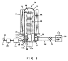
- FIG. 1 is explanatory drawings showing the configuration of an example of a batch-operating vertical apparatus for oxidation treatment employed in the oxide film formation method according to the present invention.
- the oxidation treatment apparatus 10 comprises a reaction vessel 12 which is cylindrical and vertically extended, has a single tubular structure closed at the top thereof and is composed of silicon dioxide or the likes.
- a manifold 13 is positioned which is a cylindrical stainless steel and tightly joined to the lower end of said reaction vessel 12.
- a cover member 14 is positioned which can be shifted up and down by a boat elevator (not shown).
- a wafer boat 15 which is composed of silicon dioxide for example is mounted on the cover member 14A.
- a plurality of the semiconductor wafers 16 consists of silicon for example, on each of which oxide film is to be formed , are held at regular intervals in a vertical direction on the wafer boat 15.
- the wafers 16 held on said wafer boat 15 are positioned in a processing area PA inside the reaction vessel 12.
- the reaction vessel 12 is about the size that a cylindrical space D is to be defined between the inner surface of the reaction vessel 12 and the wafer boat 15 or the outer circumferential rim of the wafer 16 after the wafer boat 15 is inserted into the reaction vessel 12.
- This cylindrical space D is configured to have a size of approximately 20 to 50mm for example to obtain desired exhaust conductance within said reaction vessel 12 considering after-mentioned gas flow rate and pressure inside the reaction vessel 12.
- a warm-up heater 17 comprising a resistance heating element is provided around the reaction vessel 12 to encircle said reaction vessel 12, and this warm-up heater 17 applies heat for the temperature inside the reaction vessel 12 or the temperature of the positioned wafer 16 to reach a predetermined preset temperature.
- a processing gas supply pipe 18 is provided piercing through the peripheral wall of said manifold 13.
- Teflon is used for its resistance to corrosion.
- An end portion 18a of this processing gas supply pipe 18 which is positioned inside the manifold 13 includes a processing gas induction part 18b which is bended and extended upward, and the opening at the end of the processing gas induction part 18b is positioned to face upward at the lower end of the cylindrical space D of the reaction vessel 12.
- a processing gas is basically supplied upward toward the cylindrical space D and then, by diffusion upon reaching the upper end (ceiling) of the reaction vessel 12 for example, supplied to the processing area PA where the wafer 16 is positioned.
- the ozone generator 19 in this example is equipped with a plasma generator for example and forms ozone from oxygen.
- a purifier 20 to which an oxygen gas supply pipe 21 and an additive gas supply pipe 22 are connected.
- the oxygen gas from the oxygen gas supply pipe 21 and the additive gas, in the form of a nitrogen gas or a carbon dioxide gas, from the additive gas supply pipe 22 have suitable conditions for forming ozone in terms of purity.
- gases are supplied to the ozone generator 19 in the conditions which are satisfied in reducing the production of impurities, a corrosive gas by moisture in particular.
- a vent 23 is provided on the manifold 13 at the opposite side of where the processing gas supply pipe 18 pierces through, and an exhaust pipe 24 is connected to the vent 23, and a vacuum pump 26 is connected to the exhaust pipe 24 with a combination valve 25 inserted therebetween.
- the vacuum pump 26 exhausts the reaction vessel 12 of gas through the exhaust pipe 24 and keeps the reaction vessel 12 depressurized inside, and the combination valve 25 functions by adjusting the opening thereof to control the pressure inside the reaction vessel 12.
- a nitrogen gas supply pipe 27 is connected to the manifold 13 in the lower position of the vent 23 to supply a nitrogen gas for example.
- a second processing gas supply pipe 32 is provided in the manifold 13.
- the second processing gas supply pipe 32 may have an end portion 32a which is bended an extended upward, and the opening of the end is positioned to face upward at the lower end of the cylindrical space D of the reaction vessel 12 along with the processing gas induction part 18b.
- the second processing gas supply pipe 32 supplies processing gases as necessary for various kinds of processing and is used as an oxygen gas supply pipe, for example.
- a control mechanism (not shown) is provided to control the operating conditions of each of the above-mentioned ozone generator 19, purifier 20, oxygen gas supply pipe 21, additive gas supply pipe 22, combination valve 25, vacuum pump 26, nitrogen gas supply pipe 27, second processing gas supply pipe 32, etc.
- this control mechanism is equipped with a microprocessor, a process controller, etc. and functions to measure the parameters of the processing condition of the oxidation treatment apparatus 10 such as the temperature and pressure of each section and send control signals to each section accordingly based on the measurement data.
- an oxide film is formed on the surface of a wafer by processing the wafer as described below with the oxidation treatment apparatus 10 having the above-mentioned structure.
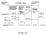
- Fig. 2 is a sequence diagram schematically showing a specific process of the method for the formation of oxide films according to the present invention.
- the method for the formation of oxide films according to the present invention has three steps consisting of a precleaning process as the first step, a pretreatment process from loading down to the third step as the second step, and an oxide film formation step (hereinafter referred to as a "film formation process") as the third step.
- This precleaning process is a process of cleaning the surface of the wafer on which an oxide film is to be formed.
- the surface of the wafer is cleaned by being immersed in a hydrofluoric acid solution of low concentration, for example, to mainly remove the oxides formed on the surface of the wafer.
- the temperature may be 23°C and the concentration of the chemical liquid may be 1 vol. % in the process, for example.
- the pretreatment process has 4 steps including:
- the subject wafer is loaded into the reaction vessel of the oxidation treatment apparatus and positioned in the processing area PA.
- the wafer boat 15 holding the wafer 16 after being cleaned in the precleaning process is mounted on the cover member 14 staying down.
- the temperature inside the reaction process chamber PC is controlled at an established predetermined loading temperature of t1 by heat application with the warm-up heater 17 as necessary.
- the temperature t1 for loading ranges from 25°C (a room temperature) to 600°C, for example.
- the temperature t1 for loading preferably is within the range from 50 to 550°C and 200 to 400°C in particular, depending on the kinds or conditions of the means for forming protective oxide films actually employed.
- the wafer boat 15 is loaded into the reaction vessel 12 by lifting the cover member 14 using the boat elevator, not shown, thereby positioning the wafer 16 in the processing area PA inside the reaction vessel 12 (loading), and at the same instant, the reaction process chamber PC is sealed because the opening of the lower end of the manifold 13 is closed with the cover member 14.
- the adjusting-processing-parameter operation is performed following the above-mentioned loading operation to suitably condition inside the reaction process chamber PC for the protective-oxide-film-forming operation.
- the operation is performed to provide an atmosphere of reduced pressure inside the reaction process chamber PC.
- Gas is exhausted from the reaction process chamber PC until the pressure inside the reaction vessel 12 reaches the pressure level of the predetermined reduced pressure, e.g. 13.3 to 26600 Pa (0.1 to 200 Torr), from the normal pressure of 101080 Pa (760 Torr).
- the predetermined reduced pressure e.g. 13.3 to 26600 Pa (0.1 to 200 Torr)
- the temperature inside the reaction process chamber PC is being controlled to have the established predetermined temperature t2 for forming protective oxide films by heat application with the warm-up heater 17 as necessary.
- the targeted value of the temperature inside the reaction process chamber PC is the temperature t2 for forming protective oxide films in the following protective-oxide-film-forming operation.
- the above depressurization operation and heating operation are run for the necessary time period, e.g. approximately 10 to 20 minutes, for the state of the predetermined pressure and temperature inside the reaction process chamber PC to be stable so that the condition inside the reaction process chamber PC is stabilized.
- This operation is performed to form a protective oxide film on the surface of a wafer under the conditions that the pressure and temperature inside the reaction process'chamber PC is stable as described above.
- the supply of a nitrogen gas from the nitrogen gas supply pipe 27 is ceased and an oxygen gas of a predetermined amount is supplied to the purifier 20 from the oxygen gas supply pipe 21 at a flow rate of 1 to 10 slm for example, and concurrently a nitrogen gas of a predetermined amount is supplied to the purifier 20 from the additive gas supply pipe 22 at a flow rate of 0.008 to 0.08 slm for example.
- the supplied oxygen gas and nitrogen gas have suitable conditions for forming ozone and are supplied to the ozone generator 19.
- ozone gas is produced by plasma, for example, acting on the supplied oxygen gas through a plasma generator. Then, a processing gas containing e.g. 2 to 18 vol. % of ozone is supplied from the ozone generator 19 through the processing gas supply pipe 18 to be blown upward in the cylindrical space D inside the reaction vessel 12 from the processing gas induction part 18b.
- the supply flow rate of the processing gas containing ozone shall be satisfying to form a desired protective oxide film on the wafer positioned in the processing area PA and can be established corresponding to different conditions in actuality: to cite instances, within the range approximately from 1 to 10 slm.
- a method for producing radical oxidative species, a method can be employed wherein a hydrogen gas (H 2 ) and an oxygen gas (O 2 ) are supplied directly to the reaction process chamber PC at reduced pressure.
- a hydrogen gas and an oxygen gas may be supplied at a ratio of 0.1:99.9 or 99.9:0.1 at a pressure of 13.3 to 133 Pa.
- the above processing gas supply is accomplished under the conditions that the temperature inside the reaction process chamber PC is maintained at the temperature t2 for forming protective oxide films and the pressure is controlled as well.
- the temperature t2 for forming protective oxide films is within the range or 25°C (a room temperature) to 600°C for example, lower than the temperature t3 for forming oxide films in the following process of oxide film formation in general.
- the range depends on the kinds or conditions of the means for forming protective oxide films actually employed, 50 to 550°C is preferable and 200 to 400°C in particular is preferable.
- This temperature t2 for forming protective oxide films may be the same as or different from the above-mentioned temperature t1 for loading, but preferably the temperature t2 for forming protective oxide films is the same as the temperature t1 for loading in actuality because, in this case, problems accompanied with change of temperature conditions such as causing defects in the formed protective oxide films for example can be averted and also the protective-oxide-film-forming operation can be started with high time efficiency as the established temperature inside the reaction process chamber PC is not changed.
- the pressure inside the reaction process chamber PC is maintained under depressurized conditions, e.g. 13.3 to 101080 Pa (0.1 to 760 Torr).
- this protective-oxide-film-forming operation is performed within a controlled time frame.
- the processing gas is supplied into the reaction process chamber PC only for a controlled time period.
- This protective-oxide-film-forming operation time is set for 1 to 130 minutes, for example.
- oxygen atom radicals as radical oxidative species are produced due to the activated ozone inside the reaction process chamber PC as ozone is contained in the supplied processing gas, and since the oxygen atom radicals make contact with the wafer 16, the organic matters on the surface of said wafer 16 are removed and also a protective oxide film is formed on the surface of said wafer 16.
- the film thickness of the formed protective oxide film will be thin with dense texture and also uniform since the temperature inside the reaction process chamber PC is maintained at the predetermined temperature t2 for forming protective oxide films and the pressure is maintained under the predetermined depressurized conditions.
- the film thickness of formed protective oxide films is 0.1 to 5 nm for example, preferably 0.5 to 2 nm in particular.
- the reaction vessel 12 has a single tubular structure in a state that the cylindrical space D is defined between the inner peripheral wall of the reaction vessel 12 and the outer circumferential rim of the wafer 16 so that preferable exhaust conductance can be obtained which enables to maintain the activated state of ozone stable and also maintain inside said reaction process chamber PC under the predetermined depressurized conditions.
- the preferable fact in improving the conductance inside the reaction process chamber PC is that the processing gas supply pipe 18 has at its end portion the processing gas induction part 18b bended and extended upward and also the vent 23 is positioned at the opposite side of the processing gas supply pipe 18.
- a processing gas can evenly be supplied to the wafer 16 in the processing area PA by supplying the processing gas upward toward the cylindrical space D encircling the outer circumference of the processing area PA in which the wafer 16 is positioned. This is because the flow velocity of the processing gas is reduced in the processing area PA and therefore has hardly any impact caused by the flow velocity distribution at the blow into the reaction process chamber PC.
- ozone generator 19 high ozone production efficiency can be obtained by supplying a nitrogen gas as well as an oxygen gas. Moreover, although a processing gas will contain nitrogen oxides (NOx) due to the nitrogen gas supply, contamination inside the reaction process chamber PC due to corrosion of the processing gas supply pipe 18 can be avoided by using Teflon pipe material for the processing gas supply pipe 18 to obtain high resistance to corrosion against the contained nitrogen oxides.
- NOx nitrogen oxides
- the heating operation is performed on the wafer 16, on which a protective oxide film is formed by the above protective-oxide-film-forming operation, to allow for transfer to the film formation process which is an original purpose.
- This heating operation may be proceeded to the competent condition for the intended film formation process to be initiated.
- heat is applied in this heating operation for inside the reaction process chamber PC to reach the level of the required atmospheric condition for the film formation process, i.e. to reach the preset temperature for the film formation process.
- the examples of the heating rate inside the reaction process chamber PC is not specifically limited but within the range from 20 to 200°C/min., preferably 50 to 150°C.
- the pressure inside the reaction process chamber PC is controlled corresponding to the preset pressure in the film formation process.
- the pressure is controlled to within 13.3 to 101080 Pa (0.1 to 760 Torr) and the partial pressure of oxygen is controlled to equal to or less than 1000 Pa for example, under the condition that supply of the processing gas containing ozone is ceased and an oxygen gas or an oxygen gas and a nitrogen gas are supplied through the second processing gas supply pipe 32 at a controlled flow rate.
- a protective oxide film is formed on the surface of a wafer inside the reaction process chamber PC under controlled conditions which the film formation process can directly follow.
- the film formation process is a primary process for the purpose of forming the intended oxide films on the above wafers.
- this film formation process is performed by providing an oxidation treatment wherein the temperature of a wafer is raised under depressurized conditions in the atmosphere inside the reaction process chamber PC with oxygen.
- oxidation treatment are not specifically limited, and the known conventional means for forming oxide films can be employed without modification.
- the means to be employed can be selected from or in combination of, for example, a wet oxidation method using water vapor, a dry oxidation method using ozone or other gases containing oxygen, an internal combustion method using a oxidizing gas obtained by combustion of proper gas inside the reaction process chamber, an oxidation method with radical oxidative species and an oxidation method with the atmosphere containing hydrogen chloride.
- the pressure inside the reaction process chamber may be within 133 to 101080 Pa (1 to 760 Torr) depending on the employed oxidation treatment means, and the temperature is generally set at the range from 750 to 1100°C.
- An oxide film is formed on the surface (on the continued area of a protective oxide film, to be exact) of a wafer through this film formation process, and this oxide film offers quite high quality by being formed in the film formation process for the wafer on which a protective oxide film is formed under the above-mentioned particular conditions, and further offers high uniformity in film thickness and film quality over the entire wafer even in a case of a thin film with film thickness of 5 nm for example.
- the present method for the formation of oxide films is effective as a method for forming gate-insulating films composing transistor chips, and said gate-insulating films will have favorable characteristics and long life.
- the film formation process is allowed to be run in a state with a wafer still positioned inside the reaction process chamber PC after completion of the pretreatment process, i.e. without removing the wafer out. Therefore, the protective-oxide-film-forming operation is so-called an in-situ operation (in-situ: continuous processing with the same apparatus) from the viewpoint with a focus on the film formation process.
- an in-situ operation in-situ: continuous processing with the same apparatus
- the film formation process is preferably performed by a dry oxidation method since the protective-oxide-film-forming operation is performed with the processing gas containing ozone. In this case, many of the facilities can be shared in the protective-oxide-film-forming operation and the film formation process.
- the processing may be performed for 1 to 300 minutes under the conditions that the temperature is 750 to 1100°C and the pressure is 133 to 101080 Pa (1 to 760 Torr), for example.
- the pressure returns to normal and the temperature is lowered to 25 to 600°C inside the reaction process chamber PC by supplying a predetermined amount of nitrogen gas, e.g. for approximately 15 minutes at a flow rate of 20 slm, through the nitrogen gas supply pipe 27.
- the cover member 14 is brought down by actuating the boat elevator, and thus unloading is performed in the form the wafer boat 15 ejected from the reaction process chamber PC.
- the present invention can be realized with an oxidation treatment apparatus for single wafer processing, for example.
- the structure of the reaction vessel etc. constructing the reaction process chamber is limitless, and for example a double-pipe structure comprising an inner pipe and an outer pipe may be employed.
- the precleaning process was performed in a hydrofluoric acid solution of 1 vol% concentration at a temperature of 23°C by over-etching by 30% of the sacrificial oxide film of a silicon wafer with diameter of 8 inches.
- the 100 pieces of wafers obtained by the precleaning process were held on the wafer boat 15 made of silicon dioxide which was then mounted on the cover member 14, and while the temperature was controlled at 300°C and the pressure at 101080 Pa (760 Torr) inside the reaction process chamber PC with a nitrogen gas at a flow rate of 19.8 slm and an oxygen gas at a rate of 0.2 slm being supplied to the reaction process chamber PC, said cover member 14 was inserted into the reaction vessel 12 at a room temperature to position wafers 16 in the processing area PA.
- the pressure inside the reaction process chamber PC was reduced to 13.3 Pa or less by a depressurization operation, and the temperature inside the reaction process chamber PC was maintained at 300°C as the preset temperature for forming protective oxide films t2 by controlling the warm-up heater 17.
- the processing gas containing ozone at a concentration of 14 volume percent was obtained from the ozone generator 19 by supplying an oxygen gas from the oxygen gas supply pipe 21at a rate of 1 slm and supplying a nitrogen gas from the additive gas supply pipe 22 at a rate of 0.008 slm to the purifier 20, and this processing gas containing ozone was supplied into the reaction process chamber PC maintained at a temperature of 300°C and at a pressure of 26.6 Pa (0.2 Torr) at a rate of 1 slm. This operation was continued for 9 minutes.
- the heating operation was performed in a state that the wafers 16 were still positioned inside the reaction vessel 12.
- the temperature inside the reaction process chamber PC was raised to 850°C by actuating the warm-up heater 17 at a heating rate of 100°C/min while supply of the processing gas containing ozone was ceased and an oxygen gas was supplied from the second processing gas supply pipe 32 at a rate of 0.5 slm.
- the film formation process was performed for 20 minutes under the conditions that the temperature was 850°C and the partial pressure of oxygen was 2660 Pa (20 Torr pressure) with the oxygen gas supply from the second processing gas supply pipe 32 maintained at the rate of 0.5 slm.
- the pressure was returned to normal and the temperature was lowered to 300°C inside the reaction process chamber PC by supplying a nitrogen gas from the nitrogen gas supply pipe 27 at a rate of 20 slm for 15 minutes, and then the wafer boat 15 was ejected from the reaction process chamber PC by bringing the cover member 14 down by actuating the boat elevator.
- a nitrogen gas from the nitrogen gas supply pipe 27 at a rate of 20 slm for 15 minutes
- the wafer boat 15 was ejected from the reaction process chamber PC by bringing the cover member 14 down by actuating the boat elevator.
- the characteristics of the oxide films obtained in the above way were examined with an NMOS capacitor prepared. That is to say, the range of the leakage current variation at an electric field intensity of -3 MV/cm within the wafer was examined on each oxide film of the total of 112 chip sections formed on one wafer to find out that the range was within 8% on the basis of the mean value, as shown in Fig. 4.
- a protective oxide film with a mean thickness of 0.8 nm was formed on a silicon wafer from the same lot by immersion in a hydrochloric acid solution at 60°C for 10 minutes, the ratio of H 2 O 2 :HCl:H 2 O of the solution being 1 : 1 : 5. Then an oxide film was formed on this wafer to prepare a control sample by running the process of oxide film formation (film formation process) by a dry oxidation method under exactly the same conditions as the above embodiment except for the protective-oxide-film-forming operation, and the leakage current variation within the wafer was examined likewise to obtain the result of 23% as shown in Fig. 4.
- the formed oxide film can obviously have high uniformity in film thickness and film quality over the entire wafer according to the method for the formation of oxide films of the above-mentioned embodiment.
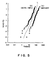
- Fig. 5 illustrates the Weibull plot of TDDB data in which the plot group (A) shows the results of the above-mentioned embodiment and the plot group (B) shows the results of the above-mentioned control sample.
- the L is a boundary line between the plot groups (A) and (B).
- the TDDB testing was performed under the conditions that the stress was maintained at -12.5 MV/cm and the chuck temperature was maintained at 120°C, and the capacitor area was 1 x 10 -4 cm 2 .
- the life as an insulating film in the form of the oxide film of a wafer obtained in the above-mentioned embodiment obviously is longer to a large extent compared to the film in the form of the control sample.
- oxide films formed according to the method for the formation of oxide films of the present invention are used as gate-insulating films composing transistor chips for example, it is to be recognized that the transistor chips maintain the performance for extended period of time and attain high reliability.
- the quality oxide film with high uniformity in film thickness and film quality over the entire area can be formed on the surface of a wafer with advantage according to the method for the formation of oxide films of the present invention.
Landscapes
- Formation Of Insulating Films (AREA)
- Insulated Gate Type Field-Effect Transistor (AREA)
Abstract
To provide a method for the formation of oxide
films to form with advantage a high-quality oxide film
having excellent uniformity in film thickness and film
quality over the entire wafer. The method for the
formation of oxide films comprises: the pretreatment
process of forming a protective oxide film on the
surface of a wafer positioned in a reaction vessel by
performing oxidation treatment with radical oxidative
species or an atmosphere containing radical oxidative
species under depressurized conditions; and the oxide-film-formation
process of forming an oxide film on the
wafer by performing oxidation treatment at a
predetermined temperature under depressurized conditions.
The oxide-film-formation process is preferably performed
following the pretreatment process in a continuous
manner in the reaction vessel in which the pretreatment
process is performed. The pretreatment process is
preferably performed at a temperature lower than the
temperature for the oxide-film-formation process and
also preferably performed under depressurized conditions,
the level of the depressurization being higher than the
level for the oxide-film-formation process. A high-quality
gate-insulating film for a transistor chip can
be formed according to this method for the formation of
oxide films.
Description
The present invention relates to a method for
forming an oxide film on the surface of a wafer composed
of silicon for example.
In manufacturing of semiconductor devices,
various kinds of processing are done on semiconductor
wafers consisting of silicon or the like, and the
processing includes oxidization processing to form an
oxide film on the surface of the wafer. The formed oxide
film functions as a gate-insulating film of transistor
chip, for example. The gate-insulating films are needed
in recent years to be thin in film thickness together
with long-running high reliability.
Generally, the oxide film formation on a wafer is
processed by placing a wafer inside a reaction vessel
heated to a high temperature, e.g. 750 to 1100°C, in the
presence of oxygen under the conditions of normal or
reduced pressure. And the oxide film formation method
under depressurized conditions particularly has an
advantage that the generating rate of oxide film is
small due to the low oxygen concentration whereby the
more degrees of freedom for controlling the formation of
oxide film is easy even if thin film thickness is formed.
However, in such a oxide film formation process
in a low oxygen atmosphere at a high temperature, the
problem is that the oxide films obtained in the oxide
film form process turn out to have low reliability due
to the roughness formed on the surface of the wafer by
being etched or nitriding by the nitrogen gas for
generating the atmosphere of low oxygen concentration
during the time period from loading of the wafer into
the reaction vessel to the initiation of actual oxide
film formation , i.e. during the heating process to
raise the temperature of the reaction vessel or the
surface of the wafer to a predetermined temperature for
the oxidation treatment.
In particular, it is difficult to form high-quality
oxide films with high uniformity of the film
thickness and film quality over the entire area of
larger-diameter wafers which are common now.
Given such situations, the following methods are
employed to form high-quality oxide films while averting
the problems caused by the oxide film formation process
in a low oxygen atmosphere at a high temperature.
However, the above methods have the following
problems:
As stated above, the problem is that a high-quality
oxide film cannot be formed with advantage on a
wafer by the conventional oxide film formation methods.
The present invention suits to solve the problems
stated above, and the purpose of the present invention
is to provide an oxide film formation method to form
with advantage a high-quality oxide film having
excellent uniformity in film thickness and film quality
over the entire wafer.
The present invention has been completed based on
the knowledge obtained by locating the root cause of the
low reliability of an oxide film formed in the oxide
film formation process , and the root cause is that a
stable protective oxide film cannot be formed under
conditions with sufficient control before starting the
process of oxide film formation by the conventional
oxide film formation methods.
The oxide film formation method of the present
invention is characterized by comprising: a pretreatment
process of forming a protective oxide film on the
surface of a wafer positioned in a reaction vessel, the
process being performed by oxidation treatment with
radical oxidative species under depressurized conditions
or by oxidation treatment with an atmosphere containing
radical oxidative species under depressurized conditions
and a oxide film formation process to form an oxide film
on the surface of said wafer with the protective oxide
film obtained by the pretreatment process, the process
being performed by oxidation treatment at a
predetermined temperature under depressurized conditions.
In the above-mentioned method for the formation of
oxide films, the oxide film formation process is
preferably performed following the pretreatment process
in a continuous manner in said reaction vessel in which
said pretreatment process is performed.
The pretreatment process is preferably performed at
a temperature lower than the temperature for the oxide-film-formation
process, and also is preferably performed
under depressurized conditions, the level of the
depressurization being higher than the level for the
oxide film formation process.
The oxidation treatment in the pretreatment process
is preferably performed under the conditions that the
temperature is from 25 to 600°C and the pressure is from
13.3 to 101080 Pa (0.1 to 760 Torr).
The radical oxidative species used for the
oxidation treatment in the pretreatment process are
preferably produced by ozone or composed of O* (oxygen
radical species) and OH* (hydroxyl radical species).
Also, the wafer heating operation in the
pretreatment process preceded to the oxide film
formation process is preferably performed at a
temperature from 750 to 1100°C in an atmosphere with a
partial pressure of oxygen of 1000 Pa or less.
Moreover, the pressure is preferably controlled to
be from 13.3 to 101080 Pa (0.1 to 760 Torr) and the
partial pressure of oxygen is preferably controlled to
be 1000 Pa or less in the pretreatment process.
Furthermore, the oxidation treatment in the oxide
film formation process can be performed by the means
selected from a wet oxidation method, a dry oxidation
method, an internal combustion method, an oxidation
method with radical oxidative species and an oxidation
method with an atmosphere containing hydrogen chloride,
under the conditions that the pressure is from 133 to
101080 Pa (1 to 760 Torr) and the temperature is from
750 to 1100°C.
A gate-insulating film of transistor chip of the
present invention is characterized in that the film is
formed according to the above-mentioned oxide film
formation method.
Also, the method for forming gate-insulating films
of transistor chips is characterized by performing the
above-mentioned oxide film formation method.
According to the oxide film formation method of the
present invention, a high-quality oxide film having
excellent uniformity in film thickness and film quality
over the entire surface of a wafer can be formed in the
oxide film formation process since a protective oxide
film is formed on the surface of the wafer positioned
inside a reaction vessel by performing oxidation
treatment with radical oxidative species (including
oxidation treatment with an atmosphere containing
radical oxidative species) under depressurized
conditions.
This is because the formed protective oxide film is
an oxide film having sufficient uniformity in film
thickness with high film quality to guarantee the
beneficial effects that a spontaneous oxidation of a
wafer in uncontrolled state before the initiation of the
oxide film formation process can be effectively
prevented, and as a result, a quality oxide film with
high uniformity as a whole can be formed completely with
advantage even in a case that the film thickness of the
entire oxide films is thin.
A predetermined processing can hence be
accomplished with rather high efficiency by performing
the oxide film formation process following the
pretreatment process in a continuous manner in the
reaction vessel in which said pretreatment process is
performed.
Also, in the pretreatment process, the effects
stated above can assuredly be achieved by performing
said pretreatment process in a temperature lower than
the temperature for the oxide film formation process or
under depressurized conditions, the level of the
depressurization being higher than the level for the
oxide film formation process.
In the pretreatment process, the above-mentioned
effects can assuredly be achieved by performing the
oxidation treatment under the conditions that the
pressure is 13.3 to 101080 Pa (0.1 to 760 Torr) and the
temperature is 25 to 600°C, and by the radical oxidative
species produced by ozone or composed of O* (oxygen
radical species) and OH* (hydroxyl radical species),
said radical oxidative species being used for the
oxidation treatment particularly in the pretreatment
process.
Moreover, the effects stated above can assuredly be
achieved by performing the wafer heating operation
preceded to the oxide film formation process at a
temperature from 750 to 1100°C in an atmosphere with a
partial pressure of oxygen of 1000 Pa or less in the
pretreatment process.
Furthermore, the effects stated above can assuredly
be achieved by controlling the pressure to be 13.3 to
101080 Pa (0.1 to 760 Torr) and the partial pressure of
oxygen to be 1000 Pa or less in the pretreatment process.
Desired effects can be achieved by the oxidation
treatment in the oxide film formation process by any
method among a wet oxidation method, a dry oxidation
method, an internal combustion method, an oxidation
method with an atmosphere containing radical oxidative
species and an oxidation method with an atmosphere
containing hydrogen chloride, under the conditions that
the pressure is from 133 to 101080 Pa (1 to 760 Torr)
and the temperature is from 750 to 1100°C.
In addition, by forming a gate-insulating film of a
transistor chip in particular according to the above
oxide film formation method, a gate-insulating film with
favorable characteristics and long life can be obtained.
Hereinafter, the present invention will be
explained in detail with reference to the drawings.
Fig. 1 is explanatory drawings showing the
configuration of an example of a batch-operating
vertical apparatus for oxidation treatment employed in
the oxide film formation method according to the present
invention.
The oxidation treatment apparatus 10 comprises a
reaction vessel 12 which is cylindrical and vertically
extended, has a single tubular structure closed at the
top thereof and is composed of silicon dioxide or the
likes.
Below the reaction vessel 12, a manifold 13 is
positioned which is a cylindrical stainless steel and
tightly joined to the lower end of said reaction vessel
12. Below the manifold 13, a cover member 14 is
positioned which can be shifted up and down by a boat
elevator (not shown).
In this way by lifting the cover member 14 to close
the opening of the lower end of the manifold 13, a
sealed reaction process chamber PC is formed inside the
reaction vessel 12.
On the cover member 14A, a wafer boat 15 which is
composed of silicon dioxide for example is mounted. A
plurality of the semiconductor wafers 16 consists of
silicon for example, on each of which oxide film is to
be formed , are held at regular intervals in a vertical
direction on the wafer boat 15. By lifting the cover
member 14 with the boat elevator to insert the wafer
boat 15 into the reaction vessel 12, the wafers 16 held
on said wafer boat 15 are positioned in a processing
area PA inside the reaction vessel 12.
The reaction vessel 12 is about the size that a
cylindrical space D is to be defined between the inner
surface of the reaction vessel 12 and the wafer boat 15
or the outer circumferential rim of the wafer 16 after
the wafer boat 15 is inserted into the reaction vessel
12. This cylindrical space D is configured to have a
size of approximately 20 to 50mm for example to obtain
desired exhaust conductance within said reaction vessel
12 considering after-mentioned gas flow rate and
pressure inside the reaction vessel 12.
A warm-up heater 17 comprising a resistance heating
element is provided around the reaction vessel 12 to
encircle said reaction vessel 12, and this warm-up
heater 17 applies heat for the temperature inside the
reaction vessel 12 or the temperature of the positioned
wafer 16 to reach a predetermined preset temperature.
Meanwhile, in the manifold 13, a processing gas
supply pipe 18 is provided piercing through the
peripheral wall of said manifold 13. As a pipe material
of this processing gas supply pipe 18, Teflon is used
for its resistance to corrosion. An end portion 18a of
this processing gas supply pipe 18 which is positioned
inside the manifold 13 includes a processing gas
induction part 18b which is bended and extended upward,
and the opening at the end of the processing gas
induction part 18b is positioned to face upward at the
lower end of the cylindrical space D of the reaction
vessel 12.
As a result, through this processing gas induction
part 18b, a processing gas is basically supplied upward
toward the cylindrical space D and then, by diffusion
upon reaching the upper end (ceiling) of the reaction
vessel 12 for example, supplied to the processing area
PA where the wafer 16 is positioned.
Connected to the processing gas supply pipe 18 is
an ozone generator 19. The ozone generator 19 in this
example is equipped with a plasma generator for example
and forms ozone from oxygen. Connected to the ozone
generator 19 in this example is a purifier 20 to which
an oxygen gas supply pipe 21 and an additive gas supply
pipe 22 are connected.
With the purifier 20, the oxygen gas from the
oxygen gas supply pipe 21 and the additive gas, in the
form of a nitrogen gas or a carbon dioxide gas, from the
additive gas supply pipe 22 have suitable conditions for
forming ozone in terms of purity. To be more precise,
gases are supplied to the ozone generator 19 in the
conditions which are satisfied in reducing the
production of impurities, a corrosive gas by moisture in
particular.
Also, a vent 23 is provided on the manifold 13 at
the opposite side of where the processing gas supply
pipe 18 pierces through, and an exhaust pipe 24 is
connected to the vent 23, and a vacuum pump 26 is
connected to the exhaust pipe 24 with a combination
valve 25 inserted therebetween.
The vacuum pump 26 exhausts the reaction vessel
12 of gas through the exhaust pipe 24 and keeps the
reaction vessel 12 depressurized inside, and the
combination valve 25 functions by adjusting the opening
thereof to control the pressure inside the reaction
vessel 12.
A nitrogen gas supply pipe 27 is connected to the
manifold 13 in the lower position of the vent 23 to
supply a nitrogen gas for example.
Moreover, a second processing gas supply pipe 32
is provided in the manifold 13. In the same manner as
the processing gas supply pipe 18, the second processing
gas supply pipe 32 may have an end portion 32a which is
bended an extended upward, and the opening of the end is
positioned to face upward at the lower end of the
cylindrical space D of the reaction vessel 12 along with
the processing gas induction part 18b.
The second processing gas supply pipe 32 supplies
processing gases as necessary for various kinds of
processing and is used as an oxygen gas supply pipe, for
example.
In addition, a control mechanism (not shown) is
provided to control the operating conditions of each of
the above-mentioned ozone generator 19, purifier 20,
oxygen gas supply pipe 21, additive gas supply pipe 22,
combination valve 25, vacuum pump 26, nitrogen gas
supply pipe 27, second processing gas supply pipe 32,
etc. To be more precise, this control mechanism is
equipped with a microprocessor, a process controller,
etc. and functions to measure the parameters of the
processing condition of the oxidation treatment
apparatus 10 such as the temperature and pressure of
each section and send control signals to each section
accordingly based on the measurement data.
According to the present invention, an oxide film
is formed on the surface of a wafer by processing the
wafer as described below with the oxidation treatment
apparatus 10 having the above-mentioned structure.
Fig. 2 is a sequence diagram schematically
showing a specific process of the method for the
formation of oxide films according to the present
invention. As shown in this diagram, the method for the
formation of oxide films according to the present
invention has three steps consisting of a precleaning
process as the first step, a pretreatment process from
loading down to the third step as the second step, and
an oxide film formation step (hereinafter referred to as
a "film formation process") as the third step.
This precleaning process is a process of cleaning
the surface of the wafer on which an oxide film is to be
formed. To be precise, the surface of the wafer is
cleaned by being immersed in a hydrofluoric acid
solution of low concentration, for example, to mainly
remove the oxides formed on the surface of the wafer.
Although the specific parameters in this
precleaning process are not necessarily limited, the
temperature may be 23°C and the concentration of the
chemical liquid may be 1 vol. % in the process, for
example.
Other cleaning means or a combination of proper
cleaning means can be employed instead in the
precleaning process.
The pretreatment process has 4 steps including:
In the loading operation, the subject wafer is
loaded into the reaction vessel of the oxidation
treatment apparatus and positioned in the processing
area PA.
In more specific terms referring to the oxidation
treatment apparatus 10 of Fig. 1, the wafer boat 15
holding the wafer 16 after being cleaned in the
precleaning process is mounted on the cover member 14
staying down.
Meanwhile, the temperature inside the reaction
process chamber PC is controlled at an established
predetermined loading temperature of t1 by heat
application with the warm-up heater 17 as necessary. The
temperature t1 for loading ranges from 25°C (a room
temperature) to 600°C, for example.
The temperature t1 for loading preferably is within
the range from 50 to 550°C and 200 to 400°C in
particular, depending on the kinds or conditions of the
means for forming protective oxide films actually
employed.
Under these conditions, the wafer boat 15 is loaded
into the reaction vessel 12 by lifting the cover member
14 using the boat elevator, not shown, thereby
positioning the wafer 16 in the processing area PA
inside the reaction vessel 12 (loading), and at the same
instant, the reaction process chamber PC is sealed
because the opening of the lower end of the manifold 13
is closed with the cover member 14.
The adjusting-processing-parameter operation is
performed following the above-mentioned loading
operation to suitably condition inside the reaction
process chamber PC for the protective-oxide-film-forming
operation.
To be precise, the operation is performed to
provide an atmosphere of reduced pressure inside the
reaction process chamber PC.
Gas is exhausted from the reaction process chamber
PC until the pressure inside the reaction vessel 12
reaches the pressure level of the predetermined reduced
pressure, e.g. 13.3 to 26600 Pa (0.1 to 200 Torr), from
the normal pressure of 101080 Pa (760 Torr).
Concurrently with the above-mentioned
depressurization operation, the temperature inside the
reaction process chamber PC is being controlled to have
the established predetermined temperature t2 for forming
protective oxide films by heat application with the
warm-up heater 17 as necessary. In this operation, the
targeted value of the temperature inside the reaction
process chamber PC is the temperature t2 for forming
protective oxide films in the following protective-oxide-film-forming
operation.
The above depressurization operation and heating
operation are run for the necessary time period, e.g.
approximately 10 to 20 minutes, for the state of the
predetermined pressure and temperature inside the
reaction process chamber PC to be stable so that the
condition inside the reaction process chamber PC is
stabilized.
This operation is performed to form a protective
oxide film on the surface of a wafer under the
conditions that the pressure and temperature inside the
reaction process'chamber PC is stable as described above.
To be more precise, the supply of a nitrogen gas
from the nitrogen gas supply pipe 27 is ceased and an
oxygen gas of a predetermined amount is supplied to the
purifier 20 from the oxygen gas supply pipe 21 at a flow
rate of 1 to 10 slm for example, and concurrently a
nitrogen gas of a predetermined amount is supplied to
the purifier 20 from the additive gas supply pipe 22 at
a flow rate of 0.008 to 0.08 slm for example. Through
the purifier 20, the supplied oxygen gas and nitrogen
gas have suitable conditions for forming ozone and are
supplied to the ozone generator 19.
In the ozone generator 19, ozone gas is produced by
plasma, for example, acting on the supplied oxygen gas
through a plasma generator. Then, a processing gas
containing e.g. 2 to 18 vol. % of ozone is supplied from
the ozone generator 19 through the processing gas supply
pipe 18 to be blown upward in the cylindrical space D
inside the reaction vessel 12 from the processing gas
induction part 18b.
The supply flow rate of the processing gas
containing ozone shall be satisfying to form a desired
protective oxide film on the wafer positioned in the
processing area PA and can be established corresponding
to different conditions in actuality: to cite instances,
within the range approximately from 1 to 10 slm.
Also, for producing radical oxidative species, a
method can be employed wherein a hydrogen gas (H2) and an
oxygen gas (O2) are supplied directly to the reaction
process chamber PC at reduced pressure. In this method,
for example, a hydrogen gas and an oxygen gas may be
supplied at a ratio of 0.1:99.9 or 99.9:0.1 at a
pressure of 13.3 to 133 Pa.
The above processing gas supply is accomplished
under the conditions that the temperature inside the
reaction process chamber PC is maintained at the
temperature t2 for forming protective oxide films and
the pressure is controlled as well.
The temperature t2 for forming protective oxide
films is within the range or 25°C (a room temperature)
to 600°C for example, lower than the temperature t3 for
forming oxide films in the following process of oxide
film formation in general. Although the range depends on
the kinds or conditions of the means for forming
protective oxide films actually employed, 50 to 550°C is
preferable and 200 to 400°C in particular is preferable.
This temperature t2 for forming protective oxide
films may be the same as or different from the above-mentioned
temperature t1 for loading, but preferably the
temperature t2 for forming protective oxide films is the
same as the temperature t1 for loading in actuality
because, in this case, problems accompanied with change
of temperature conditions such as causing defects in the
formed protective oxide films for example can be averted
and also the protective-oxide-film-forming operation can
be started with high time efficiency as the established
temperature inside the reaction process chamber PC is
not changed.
During the protective-oxide-film-forming operation,
the pressure inside the reaction process chamber PC is
maintained under depressurized conditions, e.g. 13.3 to
101080 Pa (0.1 to 760 Torr).
Furthermore, this protective-oxide-film-forming
operation is performed within a controlled time frame.
To be more precise, the processing gas is supplied into
the reaction process chamber PC only for a controlled
time period. This protective-oxide-film-forming
operation time is set for 1 to 130 minutes, for example.
In the above-mentioned protective-oxide-film-forming
operation, oxygen atom radicals as radical
oxidative species are produced due to the activated
ozone inside the reaction process chamber PC as ozone is
contained in the supplied processing gas, and since the
oxygen atom radicals make contact with the wafer 16, the
organic matters on the surface of said wafer 16 are
removed and also a protective oxide film is formed on
the surface of said wafer 16.
Therefore, in this protective-oxide-film-forming
operation, the film thickness of the formed protective
oxide film will be thin with dense texture and also
uniform since the temperature inside the reaction
process chamber PC is maintained at the predetermined
temperature t2 for forming protective oxide films and
the pressure is maintained under the predetermined
depressurized conditions.
The film thickness of formed protective oxide films
is 0.1 to 5 nm for example, preferably 0.5 to 2 nm in
particular.
In the shown oxidation treatment apparatus 10, the
reaction vessel 12 has a single tubular structure in a
state that the cylindrical space D is defined between
the inner peripheral wall of the reaction vessel 12 and
the outer circumferential rim of the wafer 16 so that
preferable exhaust conductance can be obtained which
enables to maintain the activated state of ozone stable
and also maintain inside said reaction process chamber
PC under the predetermined depressurized conditions.
Furthermore, the preferable fact in improving the
conductance inside the reaction process chamber PC is
that the processing gas supply pipe 18 has at its end
portion the processing gas induction part 18b bended and
extended upward and also the vent 23 is positioned at
the opposite side of the processing gas supply pipe 18.
Moreover, a processing gas can evenly be supplied
to the wafer 16 in the processing area PA by supplying
the processing gas upward toward the cylindrical space D
encircling the outer circumference of the processing
area PA in which the wafer 16 is positioned. This is
because the flow velocity of the processing gas is
reduced in the processing area PA and therefore has
hardly any impact caused by the flow velocity
distribution at the blow into the reaction process
chamber PC.
In the above-mentioned ozone generator 19, high
ozone production efficiency can be obtained by supplying
a nitrogen gas as well as an oxygen gas. Moreover,
although a processing gas will contain nitrogen oxides
(NOx) due to the nitrogen gas supply, contamination
inside the reaction process chamber PC due to corrosion
of the processing gas supply pipe 18 can be avoided by
using Teflon pipe material for the processing gas supply
pipe 18 to obtain high resistance to corrosion against
the contained nitrogen oxides.
The heating operation is performed on the wafer 16,
on which a protective oxide film is formed by the above
protective-oxide-film-forming operation, to allow for
transfer to the film formation process which is an
original purpose.
This heating operation may be proceeded to the
competent condition for the intended film formation
process to be initiated.
Basically, heat is applied in this heating
operation for inside the reaction process chamber PC to
reach the level of the required atmospheric condition
for the film formation process, i.e. to reach the preset
temperature for the film formation process. The examples
of the heating rate inside the reaction process chamber
PC is not specifically limited but within the range from
20 to 200°C/min., preferably 50 to 150°C.
The pressure inside the reaction process chamber PC
is controlled corresponding to the preset pressure in
the film formation process. To be more precise, the
pressure is controlled to within 13.3 to 101080 Pa (0.1
to 760 Torr) and the partial pressure of oxygen is
controlled to equal to or less than 1000 Pa for example,
under the condition that supply of the processing gas
containing ozone is ceased and an oxygen gas or an
oxygen gas and a nitrogen gas are supplied through the
second processing gas supply pipe 32 at a controlled
flow rate.
In this heating process, although the temperature
of a wafer inside the reaction process chamber PC is
gradually raised, the wafer is protected by the
protective oxide film formed on the surface of each
wafer, thereby proceeding without control of oxidization
of wafers can effectively be prevented.
By performing the above 4-step operations of (1)
loading operation, (2) adjusting-processing-parameter
operation, (3) protective-oxide-film-forming operation
and (4) heating operation, a protective oxide film is
formed on the surface of a wafer inside the reaction
process chamber PC under controlled conditions which the
film formation process can directly follow.
The film formation process is a primary process for
the purpose of forming the intended oxide films on the
above wafers.
According to the present invention, this film
formation process is performed by providing an oxidation
treatment wherein the temperature of a wafer is raised
under depressurized conditions in the atmosphere inside
the reaction process chamber PC with oxygen.
Available means for the oxidation treatment are not
specifically limited, and the known conventional means
for forming oxide films can be employed without
modification. The means to be employed can be selected
from or in combination of, for example, a wet oxidation
method using water vapor, a dry oxidation method using
ozone or other gases containing oxygen, an internal
combustion method using a oxidizing gas obtained by
combustion of proper gas inside the reaction process
chamber, an oxidation method with radical oxidative
species and an oxidation method with the atmosphere
containing hydrogen chloride.
In this film formation process, the pressure inside
the reaction process chamber may be within 133 to 101080
Pa (1 to 760 Torr) depending on the employed oxidation
treatment means, and the temperature is generally set at
the range from 750 to 1100°C.
An oxide film is formed on the surface (on the
continued area of a protective oxide film, to be exact)
of a wafer through this film formation process, and this
oxide film offers quite high quality by being formed in
the film formation process for the wafer on which a
protective oxide film is formed under the above-mentioned
particular conditions, and further offers high
uniformity in film thickness and film quality over the
entire wafer even in a case of a thin film with film
thickness of 5 nm for example.
Since an oxide film with dense texture and still
high uniformity over the entire wafer despite the
thinness in film thickness can be formed in this fashion
according to the above-mentioned method, the present
method for the formation of oxide films is effective as
a method for forming gate-insulating films composing
transistor chips, and said gate-insulating films will
have favorable characteristics and long life.
Moreover, by the heating operation performed as the
final operation in the pretreatment process, the film
formation process is allowed to be run in a state with a
wafer still positioned inside the reaction process
chamber PC after completion of the pretreatment process,
i.e. without removing the wafer out. Therefore, the
protective-oxide-film-forming operation is so-called an
in-situ operation (in-situ: continuous processing with
the same apparatus) from the viewpoint with a focus on
the film formation process. Performing the film
formation process following the pretreatment process in
a continuous manner in the same reaction process chamber
PC in this way is highly advantageous because oxide
films are quite efficiently formed and wafers are not
contaminated.
The film formation process is preferably performed
by a dry oxidation method since the protective-oxide-film-forming
operation is performed with the processing
gas containing ozone. In this case, many of the
facilities can be shared in the protective-oxide-film-forming
operation and the film formation process.
Although the conditions in the case of performing
the film formation process by a dry oxidation method are
not specifically limited, the processing may be
performed for 1 to 300 minutes under the conditions that
the temperature is 750 to 1100°C and the pressure is 133
to 101080 Pa (1 to 760 Torr), for example.
When the film formation process is completed, the
pressure returns to normal and the temperature is
lowered to 25 to 600°C inside the reaction process
chamber PC by supplying a predetermined amount of
nitrogen gas, e.g. for approximately 15 minutes at a
flow rate of 20 slm, through the nitrogen gas supply
pipe 27. After that, the cover member 14 is brought down
by actuating the boat elevator, and thus unloading is
performed in the form the wafer boat 15 ejected from the
reaction process chamber PC.
Hereinbefore described is the method for the
formation of oxide films according to the present
invention, and the oxidation treatment apparatus
employed for realizing the present invention is not
specifically limited.
Although the case of employing the batch-operating
vertical apparatus for oxidation treatment structured as
shown in Fig. 1 is described above for example, the
present invention can be realized with an oxidation
treatment apparatus for single wafer processing, for
example. Also, the structure of the reaction vessel etc.
constructing the reaction process chamber is limitless,
and for example a double-pipe structure comprising an
inner pipe and an outer pipe may be employed.
The embodiment of the present invention will be
described below although the present invention is not
limited thereto.
Each of the following process was performed
basically with the oxidation treatment apparatus with
the structure shown in Fig. 1 and according to the
sequence shown in Fig. 3.
The precleaning process was performed in a hydrofluoric
acid solution of 1 vol% concentration at a
temperature of 23°C by over-etching by 30% of the
sacrificial oxide film of a silicon wafer with diameter
of 8 inches.
The 100 pieces of wafers obtained by the
precleaning process were held on the wafer boat 15 made
of silicon dioxide which was then mounted on the cover
member 14, and while the temperature was controlled at
300°C and the pressure at 101080 Pa (760 Torr) inside
the reaction process chamber PC with a nitrogen gas at a
flow rate of 19.8 slm and an oxygen gas at a rate of 0.2
slm being supplied to the reaction process chamber PC,
said cover member 14 was inserted into the reaction
vessel 12 at a room temperature to position wafers 16 in
the processing area PA.
The pressure inside the reaction process chamber
PC was reduced to 13.3 Pa or less by a depressurization
operation, and the temperature inside the reaction
process chamber PC was maintained at 300°C as the preset
temperature for forming protective oxide films t2 by
controlling the warm-up heater 17.
Then, as supply of a nitrogen gas from the
nitrogen gas supply pipe 27 was ceased, the processing
gas containing ozone at a concentration of 14 volume
percent was obtained from the ozone generator 19 by
supplying an oxygen gas from the oxygen gas supply pipe
21at a rate of 1 slm and supplying a nitrogen gas from
the additive gas supply pipe 22 at a rate of 0.008 slm
to the purifier 20, and this processing gas containing
ozone was supplied into the reaction process chamber PC
maintained at a temperature of 300°C and at a pressure
of 26.6 Pa (0.2 Torr) at a rate of 1 slm. This operation
was continued for 9 minutes.
The analysis performed afterward confirmed that a
protective oxide film with film thickness of 1 nm had
been formed on each wafer 16 by this protective-oxide-film-forming
operation.
Following the above adjusting-processing-parameter
operation, the heating operation was performed in a
state that the wafers 16 were still positioned inside
the reaction vessel 12.
To be more precise, the temperature inside the
reaction process chamber PC was raised to 850°C by
actuating the warm-up heater 17 at a heating rate of
100°C/min while supply of the processing gas containing
ozone was ceased and an oxygen gas was supplied from the
second processing gas supply pipe 32 at a rate of 0.5
slm.
Then, the film formation process was performed for
20 minutes under the conditions that the temperature was
850°C and the partial pressure of oxygen was 2660 Pa (20
Torr pressure) with the oxygen gas supply from the
second processing gas supply pipe 32 maintained at the
rate of 0.5 slm.
After that, the pressure was returned to normal and
the temperature was lowered to 300°C inside the reaction
process chamber PC by supplying a nitrogen gas from the
nitrogen gas supply pipe 27 at a rate of 20 slm for 15
minutes, and then the wafer boat 15 was ejected from the
reaction process chamber PC by bringing the cover member
14 down by actuating the boat elevator. Thus wafers on
which oxide films with the respective total film
thickness of 2.7 nm were manufactured.
The characteristics of the oxide films obtained in
the above way were examined with an NMOS capacitor
prepared. That is to say, the range of the leakage
current variation at an electric field intensity of -3
MV/cm within the wafer was examined on each oxide film
of the total of 112 chip sections formed on one wafer to
find out that the range was within 8% on the basis of
the mean value, as shown in Fig. 4.
On the other hand, a protective oxide film with a
mean thickness of 0.8 nm was formed on a silicon wafer
from the same lot by immersion in a hydrochloric acid
solution at 60°C for 10 minutes, the ratio of
H2O2:HCl:H2O of the solution being 1 : 1 : 5. Then an oxide
film was formed on this wafer to prepare a control
sample by running the process of oxide film formation
(film formation process) by a dry oxidation method under
exactly the same conditions as the above embodiment
except for the protective-oxide-film-forming operation,
and the leakage current variation within the wafer was
examined likewise to obtain the result of 23% as shown
in Fig. 4.
Based on the results stated above, the formed oxide
film can obviously have high uniformity in film
thickness and film quality over the entire wafer
according to the method for the formation of oxide films
of the above-mentioned embodiment.
Also, reliability of the formed oxide films of the
wafer obtained in the above embodiment and the control
sample were evaluated by the constant voltage TDDB
testing. Fig. 5 shows the results.
Fig. 5 illustrates the Weibull plot of TDDB data in
which the plot group (A) shows the results of the above-mentioned
embodiment and the plot group (B) shows the
results of the above-mentioned control sample. The L is
a boundary line between the plot groups (A) and (B).
In this case, the TDDB testing was performed under
the conditions that the stress was maintained at -12.5
MV/cm and the chuck temperature was maintained at 120°C,
and the capacitor area was 1 x 10⁻⁴ cm2.
Based on the result shown in Fig. 5, the life as an
insulating film in the form of the oxide film of a wafer
obtained in the above-mentioned embodiment obviously is
longer to a large extent compared to the film in the
form of the control sample.
In a case that the oxide films formed according to
the method for the formation of oxide films of the
present invention are used as gate-insulating films
composing transistor chips for example, it is to be
recognized that the transistor chips maintain the
performance for extended period of time and attain high
reliability.
As stated above, the quality oxide film with high
uniformity in film thickness and film quality over the
entire area can be formed on the surface of a wafer with
advantage according to the method for the formation of
oxide films of the present invention.
Claims (12)
- An oxide film formation method to form an oxide film on the surface of a wafer, the method being characterized by comprising:a pretreatment process of forming a protective oxide film on the surface of a wafer positioned in a reaction vessel, the process being performed by oxidation treatment with radical oxidative species under depressurized conditions or by oxidation treatment with an atmosphere containing radical oxidative species under depressurized conditions anda oxide film formation process to form an oxide film on the surface of said wafer with the protective oxide film obtained by the pretreatment process, the process being performed by oxidation treatment at a predetermined temperature under depressurized conditions.
- An oxide film formation method according to claim 1, characterized in that the oxide film formation process is performed following the pretreatment process in a continuous manner in said reaction vessel in which said pretreatment process is performed.
- An oxide film formation method according to claim 1 or 2, characterized in that the pretreatment process is performed at a temperature lower than the temperature for the oxide film formation process.
- An oxide film formation method according to any one of claims 1 to 3, characterized in that the pretreatment process is performed under depressurized conditions, the level of the depressurization being higher than the level for the oxide film formation process.
- An oxide film formation method according to any one of claims 1 to 4, characterized in that the oxidation treatment in the pretreatment process is performed under the conditions that the temperature is from 25 to 600°C and the pressure is from 13.3 to 101080 Pa (0.1 to 760 Torr).
- An oxide film formation method according to any one of claims 1 to 5, characterized in that the radical oxidative species used for the oxidation treatment in the pretreatment process are produced by ozone.
- An oxide film formation method according to any one of claims 1 to 5, characterized in that the radical oxidative species are composed of O* (oxygen radical species) and OH* (hydroxyl radical species).
- An oxide film formation method according to any one of claims 1 to 7, characterized in that a wafer heating operation in the pretreatment process preceded to the oxide film formation process is performed at a temperature from 750 to 1100°C in an atmosphere with a partial pressure of oxygen of 1000 Pa or less.
- An oxide film formation method according to any one of claims 1 to 8, characterized in that the pressure is controlled to be from 13.3 to 101080 Pa (0.1 to 760 Torr) and the partial pressure of oxygen is controlled to be 1000 Pa or less in the pretreatment process.
- An oxide film formation method according to any one of claims 1 to 9, characterized in that the oxidation treatment in the oxide film formation process is performed by the means selected from a wet oxidation method, a dry oxidation method, an internal combustion method, an oxidation method with radical oxidative species and an oxidation method with an atmosphere containing hydrogen chloride, under the conditions that the pressure is from 133 to 101080 Pa (1 to 760 Torr) and the temperature is from 750 to 1100°C.
- A gate-insulating film of transistor chip characterized in that the film is formed by the oxide film formation method according to any one of claims 1 to 10.
- A method for forming gate-insulating films of transistor chips characterized in that the method for the formation of oxide films is performed according to any one of claims 1 to 10.
Applications Claiming Priority (3)
| Application Number | Priority Date | Filing Date | Title |
|---|---|---|---|
| JP2001055281 | 2001-02-28 | ||
| JP2001055281A JP4914536B2 (en) | 2001-02-28 | 2001-02-28 | Oxide film formation method |
| PCT/JP2002/001869 WO2002075802A1 (en) | 2001-02-28 | 2002-02-28 | Oxide film forming method |
Publications (2)
| Publication Number | Publication Date |
|---|---|
| EP1372189A1 true EP1372189A1 (en) | 2003-12-17 |
| EP1372189A4 EP1372189A4 (en) | 2005-12-28 |
Family
ID=18915484
Family Applications (1)
| Application Number | Title | Priority Date | Filing Date |
|---|---|---|---|
| EP02701646A Withdrawn EP1372189A4 (en) | 2001-02-28 | 2002-02-28 | PROCESS FOR FORMING OXIDE FILM |
Country Status (7)
| Country | Link |
|---|---|
| US (1) | US7064084B2 (en) |
| EP (1) | EP1372189A4 (en) |
| JP (1) | JP4914536B2 (en) |
| KR (1) | KR100854543B1 (en) |
| CN (1) | CN1270358C (en) |
| TW (1) | TW563181B (en) |
| WO (1) | WO2002075802A1 (en) |
Families Citing this family (12)
| Publication number | Priority date | Publication date | Assignee | Title |
|---|---|---|---|---|
| ATE353475T1 (en) * | 2002-10-11 | 2007-02-15 | Soitec Silicon On Insulator | METHOD AND DEVICE FOR PRODUCING AN ADHESIVE SUBSTRATE SURFACE |
| US7160740B2 (en) * | 2003-07-07 | 2007-01-09 | Advanced Micro Devices, Inc. | Methods of controlling properties and characteristics of a gate insulation layer based upon electrical test data, and system for performing same |
| JP4329655B2 (en) * | 2004-09-10 | 2009-09-09 | セイコーエプソン株式会社 | Semiconductor device manufacturing method and semiconductor manufacturing apparatus. |
| US20080038486A1 (en) * | 2006-08-03 | 2008-02-14 | Helmuth Treichel | Radical Assisted Batch Film Deposition |
| JP4983159B2 (en) * | 2006-09-01 | 2012-07-25 | 東京エレクトロン株式会社 | Process for oxidizing object, oxidation apparatus and storage medium |
| JP2010087475A (en) * | 2008-09-03 | 2010-04-15 | Hitachi Kokusai Electric Inc | Method and device for manufacturing semiconductor device |
| KR101851275B1 (en) * | 2008-11-28 | 2018-04-24 | 주식회사 원익아이피에스 | Method for depositing multiple metal system oxide thin film |
| JP5479304B2 (en) * | 2010-11-10 | 2014-04-23 | 信越半導体株式会社 | Method for forming thermal oxide film on silicon single crystal wafer |
| US11495437B2 (en) | 2019-05-21 | 2022-11-08 | Beijing E-Town Semiconductor Technology, Co., Ltd | Surface pretreatment process to improve quality of oxide films produced by remote plasma |
| CN111057993B (en) * | 2019-12-31 | 2022-03-18 | 中国科学院上海应用物理研究所 | Method for improving anti-tellurium corrosion performance of alloy material for molten salt reactor and an alloy part |
| TWI810561B (en) | 2020-05-14 | 2023-08-01 | 南韓商Lg電子股份有限公司 | Blower |
| CN121454000B (en) * | 2025-10-30 | 2026-08-07 | 江南造船(集团)有限责任公司 | A method for assessing the maturity of passivation film in ship pipelines |
Family Cites Families (15)
| Publication number | Priority date | Publication date | Assignee | Title |
|---|---|---|---|---|
| JPS59227128A (en) | 1983-06-08 | 1984-12-20 | Hitachi Ltd | Oxidation method for semiconductor substrate |
| JP2688653B2 (en) | 1988-05-06 | 1997-12-10 | 東京エレクトロン株式会社 | Semiconductor pressure oxidation method |
| JPH07118522B2 (en) | 1990-10-24 | 1995-12-18 | インターナショナル・ビジネス・マシーンズ・コーポレイション | Method and semiconductor structure for oxidizing a substrate surface |
| JP3210370B2 (en) | 1991-08-20 | 2001-09-17 | 忠弘 大見 | Method of forming oxide film |
| JPH05275419A (en) * | 1992-03-27 | 1993-10-22 | Mitsubishi Materials Corp | Oxidizing apparatus and method of semiconductor substrate |
| JPH06333917A (en) | 1993-05-20 | 1994-12-02 | Fujitsu Ltd | Method for pre-oxidizing semiconductor wafer |
| JPH0786271A (en) * | 1993-09-17 | 1995-03-31 | Fujitsu Ltd | Method for producing silicon oxide film |
| US6706572B1 (en) * | 1994-08-31 | 2004-03-16 | Semiconductor Energy Laboratory Co., Ltd. | Method for manufacturing a thin film transistor using a high pressure oxidation step |
| JPH09153489A (en) * | 1995-11-30 | 1997-06-10 | Toshiba Corp | Method for manufacturing semiconductor device |
| US6607946B1 (en) * | 1996-05-22 | 2003-08-19 | Micron Technology, Inc. | Process for growing a dielectric layer on a silicon-containing surface using a mixture of N2O and O3 |
| US6599847B1 (en) * | 1996-08-27 | 2003-07-29 | Taiwan Semiconductor Manufacturing Company | Sandwich composite dielectric layer yielding improved integrated circuit device reliability |
| JPH10178009A (en) | 1996-12-19 | 1998-06-30 | Sony Corp | Method for manufacturing semiconductor device |
| US6197658B1 (en) * | 1998-10-30 | 2001-03-06 | Taiwan Semiconductor Manufacturing Company | Sub-atmospheric pressure thermal chemical vapor deposition (SACVD) trench isolation method with attenuated surface sensitivity |
| US6511921B1 (en) * | 1999-01-12 | 2003-01-28 | Sumco Phoenix Corporation | Methods for reducing the reactivity of a semiconductor substrate surface and for evaluating electrical properties of a semiconductor substrate |
| US20020127883A1 (en) * | 2001-01-09 | 2002-09-12 | Conti Richard A. | Bis (tertiarybutylamino) silane and ozone based doped and undoped oxides |
-
2001
- 2001-02-28 JP JP2001055281A patent/JP4914536B2/en not_active Expired - Fee Related
-
2002
- 2002-02-27 TW TW091103888A patent/TW563181B/en not_active IP Right Cessation
- 2002-02-28 KR KR1020037011210A patent/KR100854543B1/en not_active Expired - Fee Related
- 2002-02-28 US US10/468,914 patent/US7064084B2/en not_active Expired - Lifetime
- 2002-02-28 WO PCT/JP2002/001869 patent/WO2002075802A1/en not_active Ceased
- 2002-02-28 EP EP02701646A patent/EP1372189A4/en not_active Withdrawn
- 2002-02-28 CN CNB028090187A patent/CN1270358C/en not_active Expired - Fee Related
Also Published As
| Publication number | Publication date |
|---|---|
| EP1372189A4 (en) | 2005-12-28 |
| JP4914536B2 (en) | 2012-04-11 |
| CN1518760A (en) | 2004-08-04 |
| JP2002261094A (en) | 2002-09-13 |
| TW563181B (en) | 2003-11-21 |
| WO2002075802A1 (en) | 2002-09-26 |
| KR100854543B1 (en) | 2008-08-26 |
| KR20030080230A (en) | 2003-10-11 |
| CN1270358C (en) | 2006-08-16 |
| US20040087180A1 (en) | 2004-05-06 |
| US7064084B2 (en) | 2006-06-20 |
Similar Documents
| Publication | Publication Date | Title |
|---|---|---|
| TWI393185B (en) | Film forming method and film forming device | |
| US7208428B2 (en) | Method and apparatus for treating article to be treated | |
| US7064084B2 (en) | Oxide film forming method | |
| JP3965167B2 (en) | Heat treatment method and heat treatment apparatus | |
| US20080200038A1 (en) | Heat processing method and apparatus for semiconductor process | |
| JP2002176052A (en) | Method and apparatus for oxidizing object to be treated | |
| US11749530B2 (en) | Method of removing phosphorus-doped silicon film and system therefor | |
| KR101232970B1 (en) | Heat processing method and apparatus for semiconductor process, and computer readable medium | |
| KR100848993B1 (en) | Oxidation method and apparatus for object to be processed, and recording medium | |
| JP4238812B2 (en) | Oxidizer for workpiece | |
| US7189661B2 (en) | Method of forming silicon oxynitride layer in semiconductor device and apparatus of forming the same | |
| JP4538259B2 (en) | Interlayer insulating film surface modification method and surface modification apparatus | |
| KR20060046489A (en) | Oxidation Method, Oxidation Device and Storage Media | |
| JP4361179B2 (en) | Ozone treatment apparatus and ozone treatment method | |
| JP4607347B2 (en) | Method and apparatus for processing object | |
| KR102190137B1 (en) | Method for treating substrate and apparatus for treating substrate | |
| JP3173698B2 (en) | Heat treatment method and apparatus | |
| JP4806127B2 (en) | Thin film formation method | |
| JP4626912B2 (en) | Method of processing object, processing apparatus, thin film forming method, and thin film forming apparatus | |
| US20060148223A1 (en) | Wafer surface pre-treatment with hydrogen for gate oxide formation | |
| JP3081969B2 (en) | Heat treatment method | |
| JP4506056B2 (en) | Method of nitriding object and semiconductor element | |
| JPH06151396A (en) | Cleaning method |
Legal Events
| Date | Code | Title | Description |
|---|---|---|---|
| PUAI | Public reference made under article 153(3) epc to a published international application that has entered the european phase |
Free format text: ORIGINAL CODE: 0009012 |
|
| 17P | Request for examination filed |
Effective date: 20030826 |
|
| AK | Designated contracting states |
Kind code of ref document: A1 Designated state(s): AT BE CH CY DE DK ES FI FR GB GR IE IT LI LU MC NL PT SE TR |
|
| A4 | Supplementary search report drawn up and despatched |
Effective date: 20051111 |
|
| STAA | Information on the status of an ep patent application or granted ep patent |
Free format text: STATUS: THE APPLICATION IS DEEMED TO BE WITHDRAWN |
|
| 18D | Application deemed to be withdrawn |
Effective date: 20090331 |