EP1369996A2 - Transfection high-voltage controller - Google Patents
Transfection high-voltage controller Download PDFInfo
- Publication number
- EP1369996A2 EP1369996A2 EP03017179A EP03017179A EP1369996A2 EP 1369996 A2 EP1369996 A2 EP 1369996A2 EP 03017179 A EP03017179 A EP 03017179A EP 03017179 A EP03017179 A EP 03017179A EP 1369996 A2 EP1369996 A2 EP 1369996A2
- Authority
- EP
- European Patent Office
- Prior art keywords
- coupled
- voltage
- current
- voltage current
- chemical solution
- Prior art date
- Legal status (The legal status is an assumption and is not a legal conclusion. Google has not performed a legal analysis and makes no representation as to the accuracy of the status listed.)
- Granted
Links
Images


Classifications
-
- C—CHEMISTRY; METALLURGY
- C12—BIOCHEMISTRY; BEER; SPIRITS; WINE; VINEGAR; MICROBIOLOGY; ENZYMOLOGY; MUTATION OR GENETIC ENGINEERING
- C12M—APPARATUS FOR ENZYMOLOGY OR MICROBIOLOGY; APPARATUS FOR CULTURING MICROORGANISMS FOR PRODUCING BIOMASS, FOR GROWING CELLS OR FOR OBTAINING FERMENTATION OR METABOLIC PRODUCTS, i.e. BIOREACTORS OR FERMENTERS
- C12M35/00—Means for application of stress for stimulating the growth of microorganisms or the generation of fermentation or metabolic products; Means for electroporation or cell fusion
- C12M35/02—Electrical or electromagnetic means, e.g. for electroporation or for cell fusion
-
- H—ELECTRICITY
- H03—ELECTRONIC CIRCUITRY
- H03K—PULSE TECHNIQUE
- H03K17/00—Electronic switching or gating, i.e. not by contact-making and –breaking
- H03K17/10—Modifications for increasing the maximum permissible switched voltage
- H03K17/105—Modifications for increasing the maximum permissible switched voltage in thyristor switches
-
- H—ELECTRICITY
- H03—ELECTRONIC CIRCUITRY
- H03K—PULSE TECHNIQUE
- H03K3/00—Circuits for generating electric pulses; Monostable, bistable or multistable circuits
- H03K3/02—Generators characterised by the type of circuit or by the means used for producing pulses
- H03K3/53—Generators characterised by the type of circuit or by the means used for producing pulses by the use of an energy-accumulating element discharged through the load by a switching device controlled by an external signal and not incorporating positive feedback
- H03K3/57—Generators characterised by the type of circuit or by the means used for producing pulses by the use of an energy-accumulating element discharged through the load by a switching device controlled by an external signal and not incorporating positive feedback the switching device being a semiconductor device
Abstract
Description
- The subject matter of this application is related to US Patent No. 4,750,100, and is hereby expressly incorporated by reference for all purposes.
- The present invention relates generally to transfection and cell fusion, and, more particularly, to an apparatus and method for directing high-voltage currents to a suspension of cells and DNA, usually contained in a cuvette.
- In the biotechnology field, it is known to introduce cloned DNA into mammalian and other cells using a high-voltage electrical discharge. This procedure, commonly referred to as "transfection," typically involves creation of a suspension of cells in a phosphate-buffered saline (PBS) solution and addition of cloned DNA. A high-voltage pulse applied to the suspension from a pulse generator causes the cells to take up and express the exogenous DNA. Various pulse generators are available for this purpose.
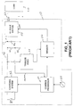
- The incorporated US patent referenced above provides a transfection high-voltage controller capable of directing a high-voltage current to a suspension of cells and DNA. Fig. 1 is a block schematic diagram of one preferred embodiment for a
transfection system 10 disclosed therein for supplying voltage and current to a load 20.Transfection system 10 includes a control processor 30, acharging system 32, atrigger feed 34, atrigger 36, a capacitor 40, afirst resistor 42, asecond resistor 44, athird resistor 46 and a hi-joule switch 50. - Control processor 30 asserts a control signal to charging
system 32 to initiate generation of a charging current.Trigger feed 34 operates on a voltage level present at an output port of the charging system.Trigger feed 34 includes a charge storage device to providetrigger 36 with an appropriate trigger energy. -
Resistor 42 is connected to the output port ofcharging system 32 and to acharging node 52.Resistor 44 is connected betweennode 52 and ground.Resistor 42 limits current flow intonode 52 to permit use of a smaller transformer incharging system 32. Capacitor 40 is coupled betweennode 52 and ground, and hi-joule switch 50 has an input terminal coupled tonode 52.Resistor 44 in series withresistor 46 gradually discharges charge stored on capacitor 40. A monitor signal for control processor 30 is generated byresistor 44 andresistor 46. - Hi-
joule switch 50 typically includes a semiconductor-controlled rectifier (SCR) (or silicon-controlled rectifier), as is well known. Hi-joule switch 50 provides an output voltage and current at its output terminal in response to an input gate signal. Once triggered, the charge/energy stored in capacitor 40 is directed through hi-joule switch 50 and into load 20 via aload line 53. Load 20 is commonly a grounded cuvette designed to contain cell suspensions, and the like. - Control processor 30 is connected to
trigger 36 and will assert a trigger signal to trigger 36. Responsive to the trigger signal, trigger 36 directs the stored trigger energy as the gating signal for hi-joule switch 50. Typically, the gating signal needs to be a higher voltage than the voltage levels conveniently produced by control processor 30. -
Transfection system 10 also includes amanual control unit 54 for setting desired voltage levels and for initiating operation. Typically,manual control unit 54 includes two independent, normally open switches, that both must be held closed in order to operate the system. Such a system reduces the risk of electrical shock to the operator. - In operation, control processor 30 asserts the control signal to the charging system when a user activates
manual control 54.Charging system 32 charges capacitor 40 to a voltage level above the prescribed voltage level set bycontrol unit 54, without triggering hi-joule switch 50 as determined by the monitor voltage. Control processor 30 deasserts the control signal to chargingsystem 32 and waits for the voltage level at node 52 (as determined from the monitor voltage) to fall to the proper level, discharged throughresistor 44 andresistor 46. When the voltage is correct, control processor 30 asserts the trigger signal to trigger 36, which in turn asserts the gating signal for hi-joule switch 50. - Responsive to the gating signal, hi-
joule switch 50 directs the charge stored on capacitor 40 to load 20 viaload line 53. The output voltage from hi-joule switch 50 is exponentially decaying, as is well known, and is a function of the capacitance of capacitor 40 and the resistance of load 20. -
Transfection system 10 is capable of supplying voltages in excess of 3,000 volts and currents in excess of 1,000 amps. Due to the magnitude of the voltages and currents involved, and the requirement that the equipment be frequently manipulated by human operators, it is a continuous objective to improve the associated safety features and procedures. - As described above,
transfection system 10 uses a semiconductor-controlled rectifier (SCR) (or silicon-controlled rectifier) hi-joule switch. This type of apparatus remains the only practical device for delivering clean waveforms at over 1000 ampere currents. Adding several SCR cells in series produces a high-voltage switch. The nature of an SCR is to deliver current up to its fusing current. Above this point, the SCR continues to deliver current, but as a dead-short. Once triggered, the SCR will not turn off until an input current drops below its holding current. - Because of the magnitude of the voltages and currents involved, it is desirable to control output current from the SCR after obtaining the desired output current. As described above, it is futile to try to limit output current by turning the SCR off when output current from the SCR reaches a desired level. Also, due to the potential range of currents involved, it is impractical to use current diverters.
- While the load resistance will vary, dependent upon many factors, there are times that the effective resistance of the load will be a minimum of about twenty ohms. The maximum voltage is typically about 2500 volts and therefore the maximum current is normally about 125 amperes. Unfortunately, because of the magnitude of the voltages, an arc-over will sometimes occur, reducing the load (cuvette) resistance to effectively zero ohms. The discharge of the transfection current without resistance can damage the equipment, fuse the SCRs and increase risks to personnel operating the equipment.
- It is known to include a limit impedance in series with the load in order to limit maximum current and to thereby decrease risks associated with arc-overs. Such a limit impedance would be added between hi-
joule switch 50 and load 20 inload line 53. Even though the series impedance is on the order of about 1.5 ohms, when the cuvette resistance is low, the limit impedance can create a significant voltage drop, altering the actual voltage level applied to the load from the desired level stored on capacitor 40. - The transfection apparatus shown in Fig. 1 includes
manual switch 54 for manually operatingtransfection system 10. In conventional systems during manual operations, it is known to require use of two pulse switches as described above. In order to charge capacitor 40, both switches must be pressed and held together. Such a system works to reduce the chance an operator will contact high voltage portions of the equipment during operation, as long as the charge and discharge processes occur without interruption. If an operator stops the operation short of capacitor discharge, then dangerous voltage levels may be present in capacitor 40. - In order to produce accurate results with
transfection system 10, a precise charge/energy must be applied to load 20. In order to accurately determine the precise charge/energy stored in capacitor 40, an accurate capacitance value is necessary. Unfortunately, because of the magnitude of the charge/energy that capacitor 40 must store, the only feasible option up to the present for producing long time constants (up to 3.5 seconds) has been to use electrolytic capacitors. It is prohibitively expensive to obtain precision film capacitors of the size required for long time constants in a transfection system. However, the use of long time constants requires maximum voltages of only 500V which is possible for electrolytics. For high-voltage (2500V) experiments, the time constant required is shorter (50 MSEC or less) so that precision (±5% or ±10%) film capacitors are feasible. As a consequence, conventional long time constant transfection systems use capacitors with a standard ±25% tolerance. The state of the art for electrolytic capacitors is about ±20%. Such variations and imprecision in capacitance of storage capacitor 40 reduce the effectiveness of conventional transfection systems since different cells may require specific time-energy delivery. - The lack of precision of electrolytic capacitors is also a problem when providing capacitor expansion modules for
transfection system 10. When usingtransfection system 10, fine control of different levels of charge/energy are required for different applications. It is desirable to provide a set of capacitors that are user selectable in order to obtain desired transfection energy profiles. - In some applications, the desired output voltage will be relatively small. While the SCR is particularly effective as a switch for high voltage and current levels, the SCR can be problematic when using low voltages. For example, sometimes the actual load can be about 1000 ohms. A typical holding current for an SCR is about 60 milliamperes. That requires that the voltage at
node 52 be greater than about 60 volts. When the voltage atnode 52 falls below 60 volts, with a 1000 ohm load, some conventional hi-joule switches will drop out and truncate the output waveform. In practice, it is desirable that operating voltages for an SCR used in the present application exceed 200 volts for best fidelity. Therefore, it is desirable to provide a hi-joule switch that is capable of operating at both high and low voltage levels. - The present invention provides apparatus and method for simply and efficiently improving prior art transfection systems. The present invention is a transfection high-voltage controller that provides features for measuring actual load resistance, and compensating for any effects of a limit impedance in series with the load. Additionally, the transfection controller of the present invention measures actual effective capacitance of a storage capacitor, or capacitors, and through use of an expansion module, effectively provides the user with a set of user-selectable capacitors having an effective ±10% tolerance when the tolerance of the individual electrolytic capacitors is ±20%.
- The preferred embodiment incorporates two sections. One section of the system handles 200-2500V and another section handles low voltages (50-500V). The transfection controller includes an improved hi-joule switch that operates in a low-voltage, high-current mode with a low dropout voltage (for use with the 500V (maximum) electrolytic capacitors. Further, additional protective circuitry in the form of a crowbar circuit, will not only prevent charging of the storage capacitor unless a safety switch is operated, charge from the capacitor is shunted to ground should the charging operation be interrupted, or if power is removed from the transfection system.
- According to one aspect of the invention, the preferred embodiment of a transfection control system for directing a high-voltage current profile to a chemical solution includes a hi-joule switch having a gate, an input and an output. A charge storing device coupled to the input provides the high-voltage current. A limit impedance between the output of the hi-joule switch and the load (chemical solution) provides arcover protection. A resistance measuring circuit is coupled to a node between the limit impedance and the chemical solution to measure resistance of the load prior to activation of the hi-joule switch. A control processor controls the voltage level at the charge storing device, and when the voltage level at the charge storing device is high enough to compensate for the drop across the limit impedance, the control processor triggers the high-joule switch. Triggering the hi-joule switch directs the stored charge into the chemical solution at the desired high-voltage level.
- According to other aspects of the invention, a crowbar switch is coupled to the charge storing device to dissipate the stored charge rapidly to ground. The crowbar is activated when a pulse switch, during manual control, is released, or when power is removed from the transfection system. The crowbar circuit permits accurate measurement of the actual capacitance, or the time constant, of the charge storing device during a procedure closely simulating actual use. This aspect of the invention includes use of a window comparator to activate an oscillator during a specific time window of charge dissipation. The time window is about equal to a period for the voltage on the charge storing device to fall to a 1/e reference value. A counter accumulates a total number of transitions from a periodic signal generated by the oscillator. The total number of transitions is proportional to the window and thus the time constant.
- By dissipating the stored charge through the crowbar circuit (and using a predetermined resistor), monitoring the voltage on the charge storage device provides a total number of transitions that is proportional to the capacitance of the charge storing device.
- According to still another aspect of the invention, a hi-joule switch includes a semiconductor-controlled rectifier (SCR) (silicon controlled rectifier) in parallel with a bipolar transistor. The SCR provides drive capacity for high-voltage currents that exceed the relatively low drive capability of the bipolar transistor. Similarly, the bipolar transistor provides low drive capability when the high-voltage current levels are less than a holding current of the SCR.
- According to yet another aspect of the invention, it includes a capacitor expansion module for use in a transfection system. The expansion module includes a plurality of capacitor cells that are electronically selectable. Each cell of the expansion module includes a capacitor, a power diode, and a power FET. The diode is coupled to the capacitor to permit discharge current only. Activation of the FET permits charging current, with capacitors being charged only in those cells having an activated FET.
- Reference to the remaining portions of the specification, including the drawing and claims, will realize other features and advantages of the present invention. Further features and advantages of the present invention, as well as the structure and operation of various embodiments of the present invention, are described in detail below with respect to accompanying drawing. In the drawing, like reference numbers indicate identical or functionally similar elements.
-
- Fig. 1 is a schematic diagram of a conventional high-voltage transfection system;
- Fig. 2 is a schematic diagram of a preferred embodiment of the present invention for a high-voltage transfection system including a load resistance measuring apparatus;
- Fig. 3 is a detailed schematic of a preferred embodiment of the resistance measuring circuit shown in Fig. 2;
- Fig. 4 is a detailed schematic diagram of a crowbar trigger circuit according to a preferred embodiment;
- Fig. 5 is a schematic diagram of a preferred embodiment of the present invention including a capacitance measuring apparatus;
- Fig. 6 is a schematic diagram of a preferred embodiment for a low-voltage, high current, low dropout hi-joule switch circuit;
- Fig. 7 is a block diagram for a trigger circuit used in the low-voltage driver of Fig. 6;
- Fig. 8 is a detailed schematic diagram of the low-voltage driver shown in Fig. 6; and
- Fig. 9 is a detailed schematic diagram of a preferred embodiment for a capacitor expansion module
-
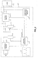
- Fig. 2 is a schematic diagram of a preferred embodiment of the present invention for a high-voltage transfection system 100 including a load-
resistance measuring apparatus 102 for measuring a resistance of aload 104. Transfection system 100 includes acontrol processor 110, acharging system 112, a hi-joule switch 114, a voltage divider 116, astorage capacitor 120, alimit resistor 122, a shunt circuit including anSCR crowbar 130 with aseries resistor 132, and anoperating control switch 134.Control processor 110 includes a microprocessor for implementing the features herein described.SCR crowbar 130 includes an SCR. -
Control processor 110 provides a charging signal to chargingsystem 112.Charging system 112 is a high-voltage switching power converter circuit that delivers essentially constant current at an output port.Storage capacitor 120 is coupled between the output port of chargingsystem 112 and ground. Voltage divider 116 is coupled between the output port of chargingsystem 112 and ground, with a tap terminal coupled to controlprocessor 110. - Hi-
joule switch 114 includes a input port (anode), an output port (cathode) and a gate port. The input port is coupled to the ungrounded terminal ofstorage capacitor 120, the gate port is coupled to controlprocessor 110, and the output port is coupled to limitresistor 122.SCR crowbar 130 includes an input port (anode), an output port (cathode) and a gate port.Series resistor 132 is coupled to the input port of hi-joule switch 114 and to the input port ofcrowbar circuit 130. The output port ofSCR crowbar 130 is coupled to ground, and the gate port is coupled to controlprocessor 110. -
Limit resistor 122 is series-coupled between the output port of hi-joule switch 114 andload 104.Limit resistor 122 typically has a very low resistance, on the order of about 1.5 ohms. In the preferred embodiment in which there is a high-voltage section (200-2500V) and a low-voltage section (50-500V), 0.5 ohms is used for the resistance of thelimit resister 122 when operating the low-voltage section and 1.5 ohms when operating the high-voltage section. Loadresistance measuring apparatus 102 is coupled to a node betweenlimit resistor 122 andload 104. Loadresistance measuring apparatus 102 includes an oscillator for generating a low-amplitude 20 KHz signal. Loadresistance measuring circuit 102 operates in well-known fashion to inject the low amplitude signal intoload 104 to establish the resistance of the load. However, the measuring system is protected against high-voltage produced during pulse delivery. Measured resistance results are provided to controlprocessor 110. - Fig. 3 is a detailed schematic diagram of a preferred embodiment for the
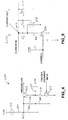
resistance measuring circuit 102 shown in Fig. 2.Resistance measuring circuit 102 includes anoscillator 150, abandpass amplifier 152, two high-voltage resistors (resistor 156 and resistor 158), four zener diodes (diode 160,diode 162,diode 164, and diode 166), and three capacitors (capacitor 170,capacitor 172, and capacitor 174). An output ofoscillator 150 is coupled throughcapacitor 170 to anode 180. A cathode ofdiode 160 is coupled tonode 180 and an anode ofdiode 160 is coupled to an anode ofdiode 162, having a cathode coupled to ground. - Resistor 156 and
capacitor 172 are coupled in series betweennode 180 and a node 182, with resistor 156 connected tonode 180 andcapacitor 172 connected to node 182. The resistance to be measured, such as for example, the resistance ofload 104 shown in Fig. 2, is coupled to node 182. -
Capacitor 174 and resistor 158 are series coupled between node 182 and a node 184, withcapacitor 174 connected to node 182 and resistor 158 connected to node 184.Diode 164 and diode 166 each include an anode and a cathode. The anodes are connected to each other, with the cathode ofdiode 164 connected to node 184 and the cathode of diode 166 connected to ground. -
Bandpass amplifier 152 includes an input, an output and a range select input (not shown). The input ofamplifier 152 is connected to node 184. The output ofamplifier 152 is connected to an analog-to-digital (A/D) converter (not shown) ofcontrol processor 110. Bandpass amplifier provides a gain of about 100-400. - In operation,
resistance measuring circuit 102 injects sine waves fromoscillator 150, having a frequency of about 20 KHz and an amplitude of about fifty millivolts, into node 182. Bandpass amplifier 152 (an AC amplifier) recovers a voltage from node 182 that is roughly proportional to the resistance ofload 104. The analog output voltage is provided to controlprocessor 110.Control processor 110 digitizes the output value fromamplifier 152. By use of a look-up table (not shown),control processor 110 linearizes the resistance values to determine the resistance ofload 104. The range select switch permitsresistance measuring circuit 102 to measure resistance in the range of 5-1,000 ohms. - Operating
control switch 134 includes two series-connected pulse switches interposed between an input ofcontrol processor 110 and ground. To operate transfection system 100, a user must press and hold each of the pulse switches ofcontrol switch 134. - In operation, operating
control switch 134 causescontrol processor 110 to assert a control signal to chargingsystem 112 to havecharging system 112 produce and deliver its output current. The output current of chargingsystem 112charges storage capacitor 120, increasing the voltage at the input of hi-joule switch 114.Control processor 110 monitors the voltage level at the input of hi-joule switch 114 via feedback from voltage divider 116. When the desired voltage level has been reached, control processor deasserts the control signal to chargingsystem 112 and triggers hi-joule switch 114.Control processor 110 triggers hi-joule switch 114 by asserting the trigger signal to the gate port. Triggering hi-joule switch 114 couples the charge/energy stored instorage capacitor 120 to load 104 throughlimit resistor 122. - Thereafter,
storage capacitor 120 discharges throughload 104 until most of its stored charge is depleted. The amount of depletion during discharge throughload 104 depends upon the holding current of hi-joule switch 114.Limit resistor 122 limits the maximum current load. - To ensure that
limit resistor 122 does not adversely affect the magnitude of the applied voltage to load 104, loadresistance measuring apparatus 102 determines the actual load resistance.Resistance measuring circuit 102 providescontrol processor 110 with the resistance measurement of the load. - Since
control processor 110 thereafter knows the actual load resistance, and the value oflimit resistor 122,control processor 110 permits the voltage level onstorage capacitor 120 to rise to a higher level to compensate for the voltage drop acrosslimit resistor 122. Providing for quantitatively-determined boosted voltage levels onstorage capacitor 120 permits transfection system 100 to produce accurate output voltages even when usinglimit resistor 122. Thelimit resistor 122 enables transfection system 100 to tolerate arc-over without damage. - Shown in Fig. 2 is the crowbar shunt circuit coupled to the input port of hi-
joule switch 114. The purpose ofSCR crowbar 130 is to dump charge stored instorage capacitor 120 by directing the stored charge to ground. In operation, asserting the trigger signal toSCR crowbar 130 causes SCR crowbar to function as a low-resistance switch.SCR crowbar 130 remains on as long as the input current exceeds the holding current. When the current decreases, SCR crowbar automatically turns itself off. Normal current levels resulting from discharge ofcapacitor 120 are typically much higher than the holding current. Thus,SCR crowbar 130 effectively removes potentially dangerous charge levels stored onstorage capacitor 120. - The use of
series resistor 132 limits the magnitude of the input current intoSCR crowbar 130. By limiting the input current intoSCR crowbar 130,SCR crowbar 130 can use smaller, less-expensive SCR devices in its construction. In the preferred embodiment,series resistor 132 has a resistance of about 1000 ohms. - As described above, transfection system 100 will only operate when
control switch 134 is properly activated.Control processor 110 will detect whether one of the pulse switches ofcontrol switch 134 is released beforecapacitor 120 is discharged through hi-joule switch 114 intoload 104. Releasing one or both of the pulse switches results incontrol processor 110 triggeringSCR crowbar 130 to remove any charge stored oncapacitor 120. - Not only is it desirable to trigger
SCR crowbar 130 should a pulse switch be released, the preferred embodiment of the present invention triggersSCR crowbar 130 should power be turned off. Fig. 4 is a detailed schematic diagram of a crowbar trigger circuit 200 according to a preferred embodiment. Trigger circuit 200, in the preferred embodiment, is incorporated intocontrol processor 110 and operates to assert trigger out should operating power be turned off. Trigger out is also asserted if a trigger crowbar input signal is asserted. - Trigger circuit 200 includes a PNP bipolar transistor Q1, an NPN bipolar transistor Q2, and a diode D1. Diode D1 is coupled to Vcc (supply voltage), which in the preferred embodiment is 17 volts. Diode D1 has an anode coupled to Vcc to conduct current from Vcc. Trigger circuit 200 includes a
resistor 201 coupled in series to a cathode of diode D1 and capacitor 202 coupled betweenresistor 201 and ground. An emitter of transistor Q1 is coupled to a node N1 betweenresistor 201 and capacitor 202. - A
capacitor 204 couples Vcc to a base of transistor Q1 and a resistor 206 couples node N1 to the base of transistor Q1. Acapacitor 208 couples the base of transistor Q1 to ground. A collector of transistor Q1 provides the trigger output signal. - A resistor 210 couples a collector of transistor Q2 to the base of transistor Q1. An emitter of transistor Q2 is coupled to ground and a base of transistor Q2 receives the trigger crowbar input signal. In the preferred embodiment, capacitor 202 is rated at about 10 microfarads and 25 volts, and
capacitor 204 andcapacitor 208 are 0.01 microfarad capacitors. - In operation, while power is provided to trigger circuit 200, current flows through diode D1 and
resistor 201 to charge capacitor 202.Capacitor 204 couples the supply voltage to the base of transistor Q1, making transistor Q1 nonconducting. Assertion of the trigger crowbar input signal turns transistor Q2 on, forcing the voltage potential at the collector of transistor Q2 low. The low potential at the collector of transistor Q2 causes the potential at the base of transistor Q1 to go low, turning it on. Turning transistor Q1 on results in Vcc providing current to assert the trigger out signal. The current is supplied from charge stored in capacitor 202, which is more slowly, and at a lower current, charged through D1 andresistor 201. - When power is removed from the system, the supply voltage drops to zero. The supply voltage level is coupled to the base of transistor Q1 by
capacitor 204. When the voltage level at the base of transistor Q1 has fallen low enough, transistor Q1 will be turned on. While supply voltage coupled to the emitter of transistor Q1 is no longer available to assert the trigger out signal, capacitor 202 is large enough to store sufficient charge to assert the trigger out signal. - As described above, asserting the trigger out signal to
SCR crowbar 130 shown in Fig. 2 removes charge fromstorage capacitor 120. A combination of the resistance ofseries resistor 132 and the capacitance ofstorage capacitor 120 defines the time constant for removing the charge fromstorage capacitor 120. As the maximum high-voltage capacitance used forstorage capacitor 120, in the preferred embodiment, is about 50 microfarads, and the resistance ofseries resistor 132 is about 1000 ohms, the worst-case time constant for discharge throughSCR crowbar 130 is about 50 milliseconds. This also reduces the chances of arc-over through the capacitor selection switch when the capacitor selection switch is changed. Various high-voltage capacitors are selected by a capacitor switch. If the switch were rotated with one capacitor partially charged, arc-over would occur. However, by the time the pulse buttons are reversed and the hand moved to select another capacitor, the SCR crowbar will have dumped the charge. - Fig. 5 is a schematic diagram of a preferred embodiment of the present invention for transfection system 100 including a capacitance measuring apparatus. As described above, transfection system 100 is a capacitive discharge system that uses large film and electrolytic capacitors to store the necessary charge used in the system. A time constant of the discharge, and the duration of the discharge is determined by the load and the particular capacitor used. An exponential waveform is desirable, as it is gentler on cells than a much-easier-to-generate square wave. Since the time constant depends on capacitance, it is desirable to obtain an actual capacitance value of the storage capacitor, at the time of use. Capacitance values change over time, and capacitance can be a function of impressed voltage and frequency. Therefore, it is desirable to provide a system that not only measures capacitance at the time of use, but also measures capacitance in a procedure that is similar to actual use.
- The use of
SCR crowbar 130 facilitates measurement of the capacitance ofstorage capacitor 120 through addition of avoltage divider 300, anamplifier 302, three voltage comparators (comparator 304,comparator 306, and comparator 308), acounter 310 and a gated oscillator 312. -
Voltage divider 300 scales the voltage present onstorage capacitor 120. The scaled voltage is provided toamplifier 302.Amplifier 302 is a buffer, and drives anode 303 at the scaled voltage level. Each of the voltage comparators,voltage comparator 304,voltage comparator 306 and voltage comparator 308, has an input coupled tonode 303.Comparator 304 is set to assert a reset signal to counter 310 when the voltage level atnode 303 exceeds a prespecified value.Comparator 306 and comparator 308 together make up a window comparator. Outputs ofcomparator 306 and comparator 308 are wired-OR to produce an AND function from the comparators and to provide a gate ON signal to gated oscillator 312 when the voltage level is between two prespecified voltage levels. An output of gated oscillator 312 is provided to counter 310. - In operation,
voltage divider 300 scales the high voltage stored onstorage capacitor 120 to a lower voltage level. It is desirable that, at the lowest output voltage, the peak of the scaled waveform be at least 220 volts.Comparator 304 is set, in well-known fashion, to assert the reset signal when the voltage level atnode 303 exceeds 220 volts. The reset signal clears counter 310. -
Comparator 306 asserts the gate signal when the voltage level atnode 303 falls below 200 volts. Similarly, comparator 308 asserts the gate signal as long as the voltage level atnode 303 exceeds (about 73.58) volts. As long as the voltage remains between 200 volts and about 73.58 volts, the gate signal is asserted to gated oscillator 312. The duration of the window represents the time for the voltage atnode 303 to drop to the time constant value because the voltage ratios are 1 / ε. For a waveformsince If this ratio of Ei / Ex = 1 / e, T = γ = time constant. Thus the window pulse-width is exactly equal to the time constant.
Counter 310 is driven by oscillator 312, and oscillator 312 only runs during the window. The value ofcounter 310 is thus proportional to the time constant. - The capacitance measuring system is produced by first charging
storage capacitor 120, and thereafter discharging it through a known resistance. If the resistance value is known, as it is when the crowbar is activated,counter 310 produces counts that are proportional to the capacitance ofstorage capacitor 120, rather than a count that is proportional to a time constant that is, in turn, a product of capacitance and resistance. However, if the crowbar is not triggered, the use of the comparators, gated oscillator and counter measures time constant directly, another parameter provided for read-out. By using the shunt circuit that includes series resistor 132 (having a known resistance), the transfection system 100 includes the desired improvement, measuring capacitance directly, measuring time constant and measuring the capacitance under conditions similar to actual use to improve accuracy. - Fig. 6 is a schematic diagram of a preferred embodiment for a low-voltage, high-current, low-dropout hi-
joule switch circuit 400.Driver circuit 400 includes anSCR 402.Driver circuit 400 may, therefore, be used in transfection system 100 shown in Fig. 2 as the hi-joule switch 114.Driver circuit 400 includes an insulated gatebipolar transistor 404 in parallel withSCR 402.Transistor 404 does not turn off with holding current. Thus, the parallel combination ofSCR 402 andtransistor 404 provide advantages of both driver types:SCR 402 provides the clean output waveforms at high voltages and currents, and thebipolar transistor 404 provides the low voltage operation.Driver circuit 400 further includes acurrent sense resistor 406 and atrigger circuit 408. -
SCR 402 includes agate 410 coupled to an output oftransistor 404, ananode 412 coupled to an input ofdriver circuit 400, and acathode 414 coupled to an output ofdriver circuit 400. A collector oftransistor 404 is coupled toanode 412, a gate oftransistor 404 is coupled to an output oftrigger 408, and an emitter oftransistor 404 is coupled togate 410. -
Current sense resistor 406couples gate 410 tocathode 414.Trigger circuit 408 receives a gating signal to activatedriver circuit 400. - In operation,
transistor 404 is made to stay on until storage capacitor 120 (shown in Fig. 2) is almost fully discharged. Transfection system 100 of Fig. 2 includes a comparator (not shown) that indicates to controlprocessor 110 when the output waveform delivered to load 104 has dropped to less than five volts. -
Transistor 404 is only operable when driving output currents up to current levels of about thirty amperes. In the preferred embodiment,current sense resistor 406 is about 0.1 ohm, allowing it to determine whentransistor 404 is driving about fifteen amperes to the output. Fifteen amperes throughcurrent sense resistor 406 produces a voltage atgate 410 sufficient to triggerSCR 402. - When
SCR 402 triggers, it effectively shorts outtransistor 404, directing most of the current at the input ofdriver circuit 400 through itself to the output. When the input voltage decreases below the holding current ofSCR 402,transistor 404 automatically resumes operation.Trigger circuit 408 is responsible for providing a sufficient voltage to operatetransistor 404 in response to the gating signal. In the preferred embodiment,trigger circuit 408 also isolates the gate voltage from ground. - Depending upon the particular application, if higher voltages are desired than is possible from a
single driver circuit 400, two or more driver circuits likedriver circuit 400 are added in series to boost output drive capability. In the preferred embodiment,driver circuit 400 incorporates a protection resistor of about 0.5 ohms (not shown) in series with the output to limit maximum current.Driver circuit 400 delivers a maximum output voltage of about 500 volts (though it is operable to about 600 volts), therefore maximum output current will be about 1000 amperes. - Fig. 7 is a block diagram for
trigger circuit 408 used indriver circuit 400 of Fig. 6. In the preferred embodiment,trigger circuit 408 includes a gated 50KHz oscillator 500 coupled to a transformer/rectifying circuit 505. - Fig. 8 is a detailed schematic diagram of low-
voltage driver 400 shown in Fig. 6 illustrating a preferred embodiment oftrigger circuit 408. In Fig. 8,oscillator 500 includes two dual-input NAND gates (NAND gate 605 and NAND gate 608), anNPN transistor 610, acapacitor 612, and four resistors (resistor 620,resistor 622,resistor 624 and resistor 626). - Resistor 620 couples the input gating signal to ground.
NAND gate 605 has a first input coupled to the ungrounded terminal of resistor 620. One terminal ofresistor 622 is coupled between the second input ofNAND gate 605 and a node 580.Resistor 624 couples an output ofNAND gate 605 to node 580. Both inputs of NAND gate 608 are coupled together and coupled to the output ofNAND gate 605.Capacitor 612 couples an output of NAND gate 608 to node 580.Resistor 626 couples the output of NAND gate 608 to a base oftransistor 610. An emitter oftransistor 610 is coupled to ground. A collector oftransistor 610 is coupled to a primary winding terminal of transformer 650 (which is coupled to 17 volts through resistor 660) of transformer/rectifier circuit 505. In response to a gate signal,oscillator 500 operates at about 50 KHz and drives transformer 650. - Transformer/
rectifier circuit 505 includes a transformer 650, adiode 652, azener diode 654, acapacitor 656, and four resistors (resistor 660,resistor 662, resistor 664 and resistor 666). Transformer 650 includes a primary winding and a secondary winding.Resistor 660 couples Vcc to a terminal of the primary winding opposite fromtransistor 610.Diode 652 andresistor 662 provide a half-wave rectifier, smoothed bycapacitor 656.Zener diode 654 regulates the output waveform at the desired voltage to drive insulated gatebipolar transistor 404. In the preferred embodiment, the voltage at the gate oftransistor 404 is about 15 volts. - Fig. 9 is a detailed schematic diagram of a preferred embodiment for a capacitor expansion module 700. An expansion module allows low-voltage (500 volt) electrolytic capacitors to be added to the transfection system 100 shown in Fig. 2 in place of storage capacitor 200. The expansion module includes a plurality of capacitors, thus it is desirable to provide for electronic switching to select particular ones of the capacitors of the expansion module. Additionally, since the electrolytic capacitors are rated for a maximum of 500 volts, and the typical maximum load is 20 ohms, the switching control of the expansion module must be able to handle 25 ampere currents. Additionally, the expansion cell desirably permits two or more capacitors to be added in parallel.
- Expansion module 700 includes a plurality of electrolytic capacitors, C1 through Cn. Each capacitor has a first terminal coupled to a charging
node 702. Charging system 112 (shown in Fig. 2) provides charging current tonode 702, in the preferred embodiment of about 200 milliamperes, peak (actually a series of 200 milliamperes peak pulses at about 35 KHz and about 33% duty cycle). Coupled to each capacitor is a cell that includes a high-power diode 703, a current limitingresistor 704 and a power FET (or insulated gate bipolar transistor) 706. In a cell, a cathode ofdiode 703 is coupled to a second terminal of capacitor Ci. Diode 703 includes an anode that is grounded. Thus, capacitor Ci can only discharge usingdiode 703. - Additionally, current limiting
resistor 704 has one terminal coupled to the cathode ofdiode 703 and a second terminal coupled to a source ofFET 706. A drain ofFET 706 is coupled to ground. A control signal activates or deactivatesFET 706, depending upon whether the capacitor Ci in its cell is to be charged. - In operation, a control signal is asserted to each
FET 706 in every cell that includes a capacitor Ci to be charged. Charging current at chargingnode 702 charges only those capacitors incells having FET 706 activated. Current does not flow throughdiode 703 during capacitor charging. Current limitingresistor 704 limits maximum current inFET 706. Current in a particular capacitor Ci can exceed the charging current maximum provided from the charging system, such as when aFET 706 is activated when another capacitor Ci in parallel stores a charge. - For discharging the capacitors Ci, it does not matter which cells have an activated
FET 706, all capacitors are discharged. Capacitors Ci discharge through diode 703 (a high power diode such as MR756) that is capable of handling current surges of over 1000 amperes for short pulses. - Thus, expansion module 700 permits only selected capacitor cells to be activated for charging in parallel, and all charged cells to be discharged, in parallel. The switching is electronically controlled and safe for the switching components. As a result, expansion module 700 uses twelve electrolytic capacitors (a 25 microfarad capacitor, a 50 microfarad capacitor, and ten 100 microfarad capacitors) to produce forty-three different capacitance values with 25 microfarad precision.
- An expansion module according to a preferred embodiment (Plus module) includes two 1100 microfarad capacitors to provide a 25-3275 microfarad range (131 values) with 25 microfarad precision. The expansion module also includes a 40 microfarad capacitor (a dither capacitor). A mode controlled by the control processor allows, by utilizing the capacitor measuring function using the SCR crowbar, the microprocessor to measure all of the capacitors. Hence, the microprocessor then has information as to the capacitance value at close to time of use. Hence, when the operator selects a desired capacitor, the microprocessor sorts out the best combination to produce the actual capacitance value desired. This procedure allows ±20% capacitors to be turned into ±10% capacitors. This procedure is an important feature of the preferred embodiment of the transfection system.
- In conclusion, the present invention provides a simple, efficient solution to a problem of molecular biology. While the above is a complete description of the preferred embodiments of the invention, various alternatives, modifications, and equivalents may be used. Therefore, the above description should not be taken as limiting the scope of the invention which is defined by the appended claims.
Claims (17)
- A method for operating a transfection system adapted to deliver a prespecified high-voltage current to a chemical solution through a protection resistor, comprising the steps of:measuring a first resistance of the chemical solution; andoperating the transfection system at a specific high-voltage current level greater than the prespecified high-voltage current to compensate for a voltage drop due to a second resistance of the protection resistor.
- A method for operating a transfection system adapted to deliver a prespecified high-voltage current to a chemical solution, comprising the steps of:asserting a trigger signal when power is removed from the transfection system;triggering a crowbar circuit coupled to a charge storage device that provides the high-voltage current when said trigger signal is asserted; anddischarging said charge storage device through said crowbar circuit when said crowbar circuit is activated.
- A method for operating a transfection system adapted to deliver a prespecified high-voltage current to a chemical solution, comprising the steps of:discharging a charge storage device, that provides the high-voltage current, through a resistor coupled to a crowbar circuit;sampling a voltage level stored on said charge storage device as said charge storage device is discharged;operating an oscillator only during a predetermined voltage range of said voltage level to provide a periodic signal;counting transitions of said periodic signal to provide a total count that is proportional to a product of said capacitance and a resistance of said resistor.
- A method for operating a transfection system adapted to deliver a prespecified high-voltage current to a chemical solution, comprising the steps of:operating a semiconductor-controlled rectifier of a hi-joule switch to direct the high-voltage current from a charge storage device to the chemical solution when the high-voltage current exceeds a threshold; andoperating a bipolar transistor of the hi-joule switch to deliver the high-voltage current when the high-voltage current is less than said threshold.
- A method for operating a transfection system adapted to deliver a high-voltage current to a chemical solution from a capacitor expansion module, with the expansion module including a plurality of capacitors coupled in parallel wherein the plurality of capacitors provide a plurality of nominal capacitance values varying from each other by a nominal increment and wherein the capacitance values each have an associated precision tolerance, comprising the steps of:including a dither capacitor in the expansion module having a nominal capacitance value not equal to an even multiple of the nominal increment and having a tolerance value equal to the associated precision tolerance;measuring an actual capacitance value of each of the plurality of capacitors of the expansion module after installation in the transfection system;selecting a desired one of the nominal capacitance values; andchoosing a combination of the plurality of capacitors that provide a combination of said actual capacitance values that vary from said desired one capacitance value less than the associated precision tolerance.
- A resistance measuring circuit for use in a transfection system to measure a load resistance of a chemical solution prior to discharge of a high-voltage current through the chemical solution, comprising:an oscillator, coupled to a node that is coupled to the chemical solution, for injecting a sinusoidal current into the chemical solution through said node;a bandpass amplifier, coupled to said node, for recovering a voltage at said node representing the resistance of the chemical solution;a first pair of anode-connected protection zener diodes coupled between an output of said oscillator and ground; anda second pair of anode-connected protection zener diodes coupled between an input of said bandpass amplifier and ground.
- An apparatus for directing a first predetermined current profile at a second predetermined high-voltage level to a chemical solution, comprising:a hi-joule switch having a gate, an input for receiving a high-voltage current, and an output for emitting a high-voltage current to a node coupled to the chemical solution;an electric charge storing device, coupled to said input of said hi-joule switch, for providing said hi-joule switch with said high-voltage current by storing a charge;a control processor, coupled to said gate of said hi-joule switch, for asserting a gating signal to activate said hi-joule switch when a voltage-level of said electric charge storing device is at least equal to the second predetermined high-voltage level; anda crowbar circuit, having an input coupled to said input of said hi-joule switch, an output coupled to a reference voltage, and responsive to a trigger signal from said control processor to a gate input, said crowbar circuit for dissipating said charge stored in said electric charge storing device when said control processor asserts said trigger signal.
- The apparatus of claim 7 wherein said control processor includes means for asserting said trigger signal when operating power is removed.
- An apparatus for directing a first predetermined current profile at a second predetermined high-voltage level to a chemical solution, comprising:a hi-joule switch having a gate, an input for receiving a high-voltage current, and an output for emitting a high-voltage current to a node coupled to the chemical solution;an electric charge storing device, coupled to said input of said hi-joule switch, for providing said hi-joule switch with said high-voltage current by storing a charge;a control processor, coupled to said gate of said hi-joule switch, for asserting a gating signal to activate said hi-joule switch when a voltage-level of said electric charge storing device is at least equal to the second predetermined high-voltage level; andmeans, coupled to said electric charge storing device, for measuring a capacitance of said electric charge storing device.
- An apparatus for directing a first predetermined current profile at a second predetermined high-voltage level to a chemical solution, comprising:a hi-joule switch having a gate, an input for receiving a high-voltage current, and an output for emitting a high-voltage current to a node coupled to the chemical solution;an electric charge storing device, coupled to said input of said hi-joule switch, for providing said hi-joule switch with said high-voltage current by storing a charge;a control processor, coupled to said gate of said hi-joule switch, for asserting a gating signal to activate said hi-joule switch when a voltage-level of said electric charge storing device is at least equal to the second predetermined high-voltage level; andmeans, coupled to said electric charge storing device, for measuring a time constant of said electric charge storing device and said load.
- The apparatus of claim 10 further comprising:wherein said control processor asserts said trigger signal to said crowbar circuit to measure a capacitance of said electric charge storing device using said time-constant measuring means.a crowbar circuit, having an input coupled to said input of said hi-joule switch by a resistor, an output coupled to a reference voltage, and responsive to a trigger signal from said control processor to a gate input, said crowbar circuit for dissipating said charge stored in said electric charge storing device when said control processor asserts said trigger signal,
- An apparatus for directing a first predetermined current profile at a second predetermined high-voltage level to a chemical solution, comprising:wherein said total count is proportional to a product of a capacitance of said electric charge storing device and a resistance through which said capacitance is discharged.a hi-joule switch having a gate, an input for receiving a high-voltage current, and an output for emitting a high-voltage current to a node coupled to the chemical solution;an electric charge storing device, coupled to said input of said hi-joule switch, for providing said hi-joule switch with said high-voltage current by storing a charge;a control processor, coupled to said gate of said hi-joule switch, for asserting a gating signal to activate said hi-joule switch when a voltage-level of said electric charge storing device is at least equal to the second predetermined high-voltage level;a voltage scaler, coupled to said electric charge storing device, for providing an output voltage to a reference node;a first voltage comparator, coupled to said reference node, for asserting a reset signal when said output voltage exceeds a first voltage level;a window comparator, coupled to said reference node, for asserting a gate signal when said output voltage is less than a second voltage level and greater than a third voltage level, wherein said second voltage level is less than said first voltage level and said third voltage level is about equal to said second voltage level divided by the base of natural logarithms (e);a counter, having an input and an output coupled to said control processor, and responsive to said reset signal, for accumulating a total count of transitions of an input signal provided at said an input and providing said control processor with said total count, wherein said reset signal clears said total count; anda gated oscillator having an output coupled to said input of said counter and gate input coupled to said window comparator and responsive to an assertion of said gate signal to generate said input signal to said counter only when said gate signal is asserted,
- The apparatus of claim 11 further comprising:wherein said control processor asserts said trigger signal to said crowbar circuit to discharge said electric charge storing device through said resistor wherein said resistor provides said resistance and said total count is proportional to said capacitance of said electric charge storing device.a crowbar circuit, having an input coupled to said input of said hi-joule switch by a resistor, an output coupled to a reference voltage, and responsive to a trigger signal from said control processor to a gate input, said crowbar circuit for dissipating said charge stored in said electric charge storing device when said control processor asserts said trigger signal,
- A hi-joule switch, comprising:a semiconductor-controlled rectifier having an anode adapted to be coupled to a source of a high-voltage current, a cathode adapted to be coupled to a chemical solution to receive said high-voltage current, and a gate for activating said semiconductor-controlled rectifier to direct said high-voltage current from said source to said chemical solution when a voltage level at said gate exceeds a first threshold, wherein said semiconductor-controlled rectifier deactivates when said high-voltage current at said anode is less than a second threshold;a trigger circuit, responsive to a gating signal, for asserting a trigger signal;a current sense resistor, coupled to said gate and to said cathode; anda bipolar transistor having a collector coupled to said anode, an emitter coupled to said cathode through said current sense resistor, and a base coupled to said trigger circuit for receiving said trigger signal, said bipolar transistor for directing said high-voltage current to said chemical solution when said high-voltage is less than said second threshold, wherein said high-voltage current directed through said current sense resistor generates a sense voltage at said gate greater than said first threshold voltage when said high-voltage current exceeds said second threshold.
- A hi-joule switch, comprising:a semiconductor-controlled rectifier having an anode adapted to be coupled to a source of a high-voltage current, a cathode adapted to be coupled to a source of a high-voltage current, a cathode adapted to be coupled to a chemical solution to receive said high-voltage current, and a gate for activating said semiconductor-controlled rectifier to direct said high-voltage current from said source to said chemical solution when a voltage level at said gate exceeds a first threshold, wherein said semiconductor-controlled rectifier deactivates when said high-voltage current at said anode is less than a second threshold;means, coupled in parallel to said semiconductor-controlled rectifier, for directing said high-voltage current to said chemical solution when said high-voltage current is less than said second threshold; andmeans, coupled to an output of said directing means and coupled to said gate and responsive to said high-voltage current, for asserting said voltage level greater than said first threshold when said high-voltage current exceeds said second threshold.
- A capacitor expansion module, comprising:wherein assertion of said control signal to selected ones of said power field-effect transistors of said plurality of control circuits permits charging of only those ones of said plurality of capacitors that correspond to said selected ones of said power field-effect transistors.a plurality of capacitors, each having a first terminal adapted to be coupled in parallel to a charging node; anda plurality of corresponding electronic control circuits, each one of said plurality of corresponding electronic control circuits coupled to a second terminal of a corresponding one of said plurality of capacitors, each corresponding electronic control circuit comprising:a power diode having an anode coupled to a reference voltage and a cathode coupled to said second terminal of said corresponding capacitor;a resistor having a first terminal coupled to said second terminal of said corresponding capacitor; anda power field-effect transistor having a drain coupled to said reference voltage, a source coupled to a second terminal of said resistor and a gate, said power field-effect transistor responsive to a control signal to permit current to flow from said source to said drain;
- A capacitor expansion module, comprising:a plurality of capacitors, each having a first terminal adapted to be coupled in parallel to a charging node; andmeans, coupled to a plurality of capacitors, for charging only selected ones of said plurality of capacitors while permitting all charged capacitors to be discharged.
Priority Applications (1)
| Application Number | Priority Date | Filing Date | Title |
|---|---|---|---|
| EP04024743A EP1515437A1 (en) | 1994-06-16 | 1995-06-13 | Transfection high-voltage controller |
Applications Claiming Priority (3)
| Application Number | Priority Date | Filing Date | Title |
|---|---|---|---|
| US08/260,654 US5642035A (en) | 1994-06-16 | 1994-06-16 | Transfection high-voltage controller |
| US260654 | 1994-06-16 | ||
| EP95304064A EP0689289B1 (en) | 1994-06-16 | 1995-06-13 | Transfection high-voltage controller |
Related Parent Applications (2)
| Application Number | Title | Priority Date | Filing Date |
|---|---|---|---|
| EP95304064.9 Division | 1995-06-13 | ||
| EP95304064A Division EP0689289B1 (en) | 1994-06-16 | 1995-06-13 | Transfection high-voltage controller |
Related Child Applications (2)
| Application Number | Title | Priority Date | Filing Date |
|---|---|---|---|
| EP04024743A Division EP1515437A1 (en) | 1994-06-16 | 1995-06-13 | Transfection high-voltage controller |
| EP04024743.9 Division-Into | 2004-10-18 |
Publications (3)
| Publication Number | Publication Date |
|---|---|
| EP1369996A2 true EP1369996A2 (en) | 2003-12-10 |
| EP1369996A3 EP1369996A3 (en) | 2004-10-13 |
| EP1369996B1 EP1369996B1 (en) | 2006-12-13 |
Family
ID=22990073
Family Applications (3)
| Application Number | Title | Priority Date | Filing Date |
|---|---|---|---|
| EP03017179A Expired - Lifetime EP1369996B1 (en) | 1994-06-16 | 1995-06-13 | Transfection high-voltage controller |
| EP95304064A Expired - Lifetime EP0689289B1 (en) | 1994-06-16 | 1995-06-13 | Transfection high-voltage controller |
| EP04024743A Withdrawn EP1515437A1 (en) | 1994-06-16 | 1995-06-13 | Transfection high-voltage controller |
Family Applications After (2)
| Application Number | Title | Priority Date | Filing Date |
|---|---|---|---|
| EP95304064A Expired - Lifetime EP0689289B1 (en) | 1994-06-16 | 1995-06-13 | Transfection high-voltage controller |
| EP04024743A Withdrawn EP1515437A1 (en) | 1994-06-16 | 1995-06-13 | Transfection high-voltage controller |
Country Status (5)
| Country | Link |
|---|---|
| US (3) | US5642035A (en) |
| EP (3) | EP1369996B1 (en) |
| JP (3) | JP3939770B2 (en) |
| CA (1) | CA2150444C (en) |
| DE (5) | DE689289T1 (en) |
Families Citing this family (21)
| Publication number | Priority date | Publication date | Assignee | Title |
|---|---|---|---|---|
| US5869326A (en) * | 1996-09-09 | 1999-02-09 | Genetronics, Inc. | Electroporation employing user-configured pulsing scheme |
| US6157171A (en) * | 1998-02-10 | 2000-12-05 | National Semiconductor Corporation | Voltage monitoring circuit for rechargeable battery |
| US6258592B1 (en) * | 1999-06-14 | 2001-07-10 | Bio-Rad Laboratories, Inc. | Electroporation cell with arc prevention/reduction |
| DE10119901A1 (en) * | 2001-04-23 | 2002-10-24 | Amaxa Gmbh | Apparatus for electrophoretic transfer of biologically active molecules into cells comprises capacitors connected to high voltage sources, which discharge via power transistor into cuvette holding sample |
| KR20030013858A (en) * | 2001-08-09 | 2003-02-15 | 삼성전자주식회사 | Regulator system for controlling output voltage and control method thereof |
| EP1461625B1 (en) * | 2001-12-06 | 2009-07-15 | Bio-Rad Laboratories, Inc. | Resistance circuit stabilization system for electroporation instruments |
| EP1607484B1 (en) * | 2004-06-14 | 2014-04-02 | Lonza Cologne GmbH | Method and circuitry for treating biological material |
| JP4619822B2 (en) * | 2005-03-03 | 2011-01-26 | 株式会社リコー | Switching regulator and voltage control method thereof |
| JP2007035873A (en) * | 2005-07-26 | 2007-02-08 | Aisin Seiki Co Ltd | Serial capacitor |
| US7923238B2 (en) * | 2006-02-10 | 2011-04-12 | Bio-Rad Laboratories, Inc. | Multi-channel electroporation system |
| JP2009538428A (en) * | 2006-05-23 | 2009-11-05 | インテグレーテッド テクノロジー コーポレーション | Protecting probe needles for high current probe testing of power devices |
| US7750605B2 (en) | 2006-09-21 | 2010-07-06 | Bio-Rad Laboratories, Inc. | Controlling an electrical signal sent to a sample load using a pulse modulated resistance |
| US7576549B2 (en) * | 2006-09-21 | 2009-08-18 | Bio-Rad Laboratories, Inc. | Methods for measuring sample resistance in electroporation |
| DE102012209582A1 (en) * | 2012-06-06 | 2013-12-12 | Robert Bosch Gmbh | Integrated controller, in particular voltage regulator, and personal protective equipment control unit |
| JP5973322B2 (en) * | 2012-10-31 | 2016-08-23 | 東芝シュネデール・インバータ株式会社 | Stored power discharge circuit of inverter device |
| DK3277368T3 (en) | 2015-03-31 | 2020-07-27 | Oncosec Medical Inc | SYSTEMS FOR IMPROVED TISSUE REGISTRATION-BASED ELECTROPORATION |
| US10095193B2 (en) * | 2015-09-11 | 2018-10-09 | The United States Of America, As Represented By The Secretary Of The Navy | High speed, high voltage (HV) capacitor system (HVCS) control systems and related methods for HVCS charge/discharge upon activation/deactivation of a HV main power system (MPS) or system fault event including a first and second timing sequence for MPS main relay(s) and HVCS relay(s) operation |
| RU2666225C1 (en) * | 2017-07-03 | 2018-09-06 | Общество с ограниченной ответственностью "научно-производственное предприятие "СибТрансНаука" | Pulsed current generator for high-voltage electrohydraulic technologies |
| RU184724U1 (en) * | 2018-08-01 | 2018-11-07 | Федеральное государственное бюджетное учреждение науки Институт сильноточной электроники Сибирского отделения Российской академии наук (ИСЭ СО РАН) | Low Inductive Capacitor Switch Assembly |
| US11071860B2 (en) * | 2019-02-06 | 2021-07-27 | Oncosec Medical Incorporated | Systems and methods for detecting fault conditions in electroporation therapy |
| EP3861863A1 (en) * | 2020-02-07 | 2021-08-11 | Bühler AG | Conductivity-adjusted device for treating cells |
Citations (4)
| Publication number | Priority date | Publication date | Assignee | Title |
|---|---|---|---|---|
| US4750100A (en) * | 1986-06-06 | 1988-06-07 | Bio-Rad Laboratories | Transfection high voltage controller |
| US4946793A (en) * | 1986-05-09 | 1990-08-07 | Electropore, Inc. | Impedance matching for instrumentation which electrically alters vesicle membranes |
| WO1991018103A1 (en) * | 1990-05-16 | 1991-11-28 | Scientific Equipment Design & Development S.C. | Method and device for making living cells permeable |
| US5232856A (en) * | 1990-06-25 | 1993-08-03 | Firth Kevin L | Electroporation device |
Family Cites Families (11)
| Publication number | Priority date | Publication date | Assignee | Title |
|---|---|---|---|---|
| US3657564A (en) * | 1970-04-24 | 1972-04-18 | Lockheed Aircraft Corp | Circuit providing fast pulse rise and fall times |
| US3955106A (en) * | 1973-12-03 | 1976-05-04 | Texas Instruments Incorporated | Multiple de-Q-ing circuit for a moving target indicator radar system |
| US4031414A (en) * | 1976-06-10 | 1977-06-21 | Gte Automatic Electric Laboratories Incorporated | Circuit arrangement for producing high current pulses |
| US5077486A (en) * | 1988-03-21 | 1991-12-31 | Gary Marson | Power supply for cathodic protection system |
| US4988942A (en) * | 1988-11-08 | 1991-01-29 | Spectra-Physics, Inc. | Switched resistor regulator control when transfer function includes discontinuity |
| DE69014398T2 (en) * | 1989-04-29 | 1995-04-20 | Fisons Plc | Method and device for optical emission spectroscopy. |
| US4999565A (en) * | 1990-01-02 | 1991-03-12 | Electric Power Research Institute | Apparatus for controlling the reactive impedance of a transmission line |
| DE4221168C1 (en) * | 1992-06-27 | 1993-11-18 | Bergwerksverband Gmbh | Igniting detonators connected in series - using ignition machine with circuit for avoiding shunt failures and limiting charge voltage of ignition capacitor dependent upon applied resistance of series connected ignition circuit |
| US5341284A (en) * | 1993-06-24 | 1994-08-23 | Hipro Electronics Co., Ltd. | Power-saving power supply unit |
| US5479337A (en) * | 1993-11-30 | 1995-12-26 | Kaiser Aerospace And Electronics Corporation | Very low power loss amplifier for analog signals utilizing constant-frequency zero-voltage-switching multi-resonant converter |
| US5479089A (en) * | 1994-12-21 | 1995-12-26 | Hughes Aircraft Company | Power converter apparatus having instantaneous commutation switching system |
-
1994
- 1994-06-16 US US08/260,654 patent/US5642035A/en not_active Expired - Lifetime
-
1995
- 1995-05-29 CA CA002150444A patent/CA2150444C/en not_active Expired - Lifetime
- 1995-06-13 DE DE0689289T patent/DE689289T1/en active Pending
- 1995-06-13 DE DE69532699T patent/DE69532699T2/en not_active Expired - Lifetime
- 1995-06-13 EP EP03017179A patent/EP1369996B1/en not_active Expired - Lifetime
- 1995-06-13 EP EP95304064A patent/EP0689289B1/en not_active Expired - Lifetime
- 1995-06-13 DE DE04024743T patent/DE04024743T1/en active Pending
- 1995-06-13 EP EP04024743A patent/EP1515437A1/en not_active Withdrawn
- 1995-06-13 DE DE69535341T patent/DE69535341T2/en not_active Expired - Lifetime
- 1995-06-13 DE DE0001369996T patent/DE03017179T1/en active Pending
- 1995-06-15 JP JP14908995A patent/JP3939770B2/en not_active Expired - Lifetime
-
1996
- 1996-04-10 US US08/630,309 patent/US5656926A/en not_active Expired - Lifetime
- 1996-04-10 US US08/630,308 patent/US5729426A/en not_active Expired - Lifetime
-
2006
- 2006-07-10 JP JP2006189815A patent/JP4185123B2/en not_active Expired - Fee Related
-
2007
- 2007-04-24 JP JP2007114748A patent/JP4185146B2/en not_active Expired - Fee Related
Patent Citations (4)
| Publication number | Priority date | Publication date | Assignee | Title |
|---|---|---|---|---|
| US4946793A (en) * | 1986-05-09 | 1990-08-07 | Electropore, Inc. | Impedance matching for instrumentation which electrically alters vesicle membranes |
| US4750100A (en) * | 1986-06-06 | 1988-06-07 | Bio-Rad Laboratories | Transfection high voltage controller |
| WO1991018103A1 (en) * | 1990-05-16 | 1991-11-28 | Scientific Equipment Design & Development S.C. | Method and device for making living cells permeable |
| US5232856A (en) * | 1990-06-25 | 1993-08-03 | Firth Kevin L | Electroporation device |
Also Published As
| Publication number | Publication date |
|---|---|
| CA2150444C (en) | 2008-05-06 |
| DE69532699D1 (en) | 2004-04-22 |
| CA2150444A1 (en) | 1995-12-17 |
| US5642035A (en) | 1997-06-24 |
| DE689289T1 (en) | 1996-08-29 |
| JP4185146B2 (en) | 2008-11-26 |
| EP1515437A1 (en) | 2005-03-16 |
| EP1369996A3 (en) | 2004-10-13 |
| JP2006288403A (en) | 2006-10-26 |
| DE04024743T1 (en) | 2005-10-20 |
| JPH08168371A (en) | 1996-07-02 |
| JP4185123B2 (en) | 2008-11-26 |
| EP0689289A3 (en) | 1997-10-08 |
| DE69532699T2 (en) | 2005-05-12 |
| US5729426A (en) | 1998-03-17 |
| JP3939770B2 (en) | 2007-07-04 |
| DE69535341D1 (en) | 2007-01-25 |
| DE69535341T2 (en) | 2007-06-28 |
| US5656926A (en) | 1997-08-12 |
| EP0689289A2 (en) | 1995-12-27 |
| EP1369996B1 (en) | 2006-12-13 |
| DE03017179T1 (en) | 2004-08-26 |
| JP2007190033A (en) | 2007-08-02 |
| EP0689289B1 (en) | 2004-03-17 |
Similar Documents
| Publication | Publication Date | Title |
|---|---|---|
| EP1369996B1 (en) | Transfection high-voltage controller | |
| US4750100A (en) | Transfection high voltage controller | |
| US5352969A (en) | Battery charging system having logarithmic analog-to-digital converter with automatic scaling of analog signal | |
| US3979657A (en) | Battery monitor with automatic scale and recycle prevents | |
| US9263241B2 (en) | Current threshold response mode for arc management | |
| US5488553A (en) | Power converter apparatus for defibrillating cardiac pacemaker | |
| US4191189A (en) | Stone disintegrator | |
| US6103084A (en) | Apparatus for electroporation | |
| US4296358A (en) | High-voltage spark source | |
| EP0512746A2 (en) | Solid state strobe tube control circuit with programmable flash pattern | |
| JPH03195485A (en) | Electropolation device | |
| CA1330106C (en) | Transfection high-voltage controller | |
| US3289064A (en) | Energy supply circuit | |
| US3767994A (en) | Circuit arrangement for rapid charging of storage batteries | |
| US4205211A (en) | Surface alloying apparatus including safety circuit | |
| US4739225A (en) | Reduced requirement energy storage for load having non-zero minimum operating potential | |
| GB2228844A (en) | High-voltage apparatus e.g. for transfection | |
| AU2003252846B2 (en) | An Electric Fence Energiser with Overload Detection | |
| SU1659061A1 (en) | For electrical therapy | |
| Polyushkin et al. | A high-voltage system of a differential spectrometer for measuring the neutron electric dipole moment |
Legal Events
| Date | Code | Title | Description |
|---|---|---|---|
| PUAI | Public reference made under article 153(3) epc to a published international application that has entered the european phase |
Free format text: ORIGINAL CODE: 0009012 |
|
| AC | Divisional application: reference to earlier application |
Ref document number: 0689289 Country of ref document: EP Kind code of ref document: P |
|
| AK | Designated contracting states |
Kind code of ref document: A2 Designated state(s): DE FR GB IT |
|
| RIC1 | Information provided on ipc code assigned before grant |
Ipc: 7C 12M 3/00 A |
|
| EL | Fr: translation of claims filed | ||
| DET | De: translation of patent claims | ||
| PUAL | Search report despatched |
Free format text: ORIGINAL CODE: 0009013 |
|
| AK | Designated contracting states |
Kind code of ref document: A3 Designated state(s): DE FR GB IT |
|
| 17P | Request for examination filed |
Effective date: 20040923 |
|
| AKX | Designation fees paid |
Designated state(s): DE FR GB IT |
|
| GRAP | Despatch of communication of intention to grant a patent |
Free format text: ORIGINAL CODE: EPIDOSNIGR1 |
|
| GRAS | Grant fee paid |
Free format text: ORIGINAL CODE: EPIDOSNIGR3 |
|
| GRAA | (expected) grant |
Free format text: ORIGINAL CODE: 0009210 |
|
| AC | Divisional application: reference to earlier application |
Ref document number: 0689289 Country of ref document: EP Kind code of ref document: P |
|
| AK | Designated contracting states |
Kind code of ref document: B1 Designated state(s): DE FR GB IT |
|
| REG | Reference to a national code |
Ref country code: GB Ref legal event code: FG4D |
|
| REF | Corresponds to: |
Ref document number: 69535341 Country of ref document: DE Date of ref document: 20070125 Kind code of ref document: P |
|
| ET | Fr: translation filed | ||
| PLBE | No opposition filed within time limit |
Free format text: ORIGINAL CODE: 0009261 |
|
| STAA | Information on the status of an ep patent application or granted ep patent |
Free format text: STATUS: NO OPPOSITION FILED WITHIN TIME LIMIT |
|
| 26N | No opposition filed |
Effective date: 20070914 |
|
| PGFP | Annual fee paid to national office [announced via postgrant information from national office to epo] |
Ref country code: GB Payment date: 20140627 Year of fee payment: 20 |
|
| PGFP | Annual fee paid to national office [announced via postgrant information from national office to epo] |
Ref country code: IT Payment date: 20140625 Year of fee payment: 20 |
|
| PGFP | Annual fee paid to national office [announced via postgrant information from national office to epo] |
Ref country code: DE Payment date: 20140627 Year of fee payment: 20 |
|
| PGFP | Annual fee paid to national office [announced via postgrant information from national office to epo] |
Ref country code: FR Payment date: 20140617 Year of fee payment: 20 |
|
| REG | Reference to a national code |
Ref country code: DE Ref legal event code: R071 Ref document number: 69535341 Country of ref document: DE |
|
| REG | Reference to a national code |
Ref country code: GB Ref legal event code: PE20 Expiry date: 20150612 |
|
| PG25 | Lapsed in a contracting state [announced via postgrant information from national office to epo] |
Ref country code: GB Free format text: LAPSE BECAUSE OF EXPIRATION OF PROTECTION Effective date: 20150612 |