EP1369909B1 - Method of fabricating a MOS transistor with reduced gate length and integrated circuit comprising such transistor - Google Patents
Method of fabricating a MOS transistor with reduced gate length and integrated circuit comprising such transistor Download PDFInfo
- Publication number
- EP1369909B1 EP1369909B1 EP03291262A EP03291262A EP1369909B1 EP 1369909 B1 EP1369909 B1 EP 1369909B1 EP 03291262 A EP03291262 A EP 03291262A EP 03291262 A EP03291262 A EP 03291262A EP 1369909 B1 EP1369909 B1 EP 1369909B1
- Authority
- EP
- European Patent Office
- Prior art keywords
- intermediate layer
- implantation
- gate
- process according
- substrate
- Prior art date
- Legal status (The legal status is an assumption and is not a legal conclusion. Google has not performed a legal analysis and makes no representation as to the accuracy of the status listed.)
- Expired - Lifetime
Links
- 238000004519 manufacturing process Methods 0.000 title description 9
- 230000002829 reductive effect Effects 0.000 title description 3
- 238000002513 implantation Methods 0.000 claims description 38
- 239000000463 material Substances 0.000 claims description 30
- 239000002019 doping agent Substances 0.000 claims description 20
- 239000000758 substrate Substances 0.000 claims description 18
- 238000000034 method Methods 0.000 claims description 16
- 230000008569 process Effects 0.000 claims description 12
- VYPSYNLAJGMNEJ-UHFFFAOYSA-N Silicium dioxide Chemical compound O=[Si]=O VYPSYNLAJGMNEJ-UHFFFAOYSA-N 0.000 claims description 11
- 229910052710 silicon Inorganic materials 0.000 claims description 7
- 239000010703 silicon Substances 0.000 claims description 7
- 239000000377 silicon dioxide Substances 0.000 claims description 7
- 235000012239 silicon dioxide Nutrition 0.000 claims description 7
- 230000003667 anti-reflective effect Effects 0.000 claims description 6
- 238000009826 distribution Methods 0.000 claims description 6
- 229910021426 porous silicon Inorganic materials 0.000 claims description 5
- 230000000284 resting effect Effects 0.000 claims description 3
- 239000004065 semiconductor Substances 0.000 claims description 3
- 229920002120 photoresistant polymer Polymers 0.000 claims description 2
- 125000006850 spacer group Chemical group 0.000 description 21
- 239000011347 resin Substances 0.000 description 8
- 229920005989 resin Polymers 0.000 description 8
- XUIMIQQOPSSXEZ-UHFFFAOYSA-N Silicon Chemical compound [Si] XUIMIQQOPSSXEZ-UHFFFAOYSA-N 0.000 description 6
- 230000000694 effects Effects 0.000 description 6
- 238000005530 etching Methods 0.000 description 6
- 230000015572 biosynthetic process Effects 0.000 description 5
- 239000006185 dispersion Substances 0.000 description 5
- 230000003071 parasitic effect Effects 0.000 description 5
- 229910052581 Si3N4 Inorganic materials 0.000 description 3
- 229910021417 amorphous silicon Inorganic materials 0.000 description 3
- 230000007423 decrease Effects 0.000 description 3
- 239000007943 implant Substances 0.000 description 3
- 230000000670 limiting effect Effects 0.000 description 3
- 230000000873 masking effect Effects 0.000 description 3
- HQVNEWCFYHHQES-UHFFFAOYSA-N silicon nitride Chemical compound N12[Si]34N5[Si]62N3[Si]51N64 HQVNEWCFYHHQES-UHFFFAOYSA-N 0.000 description 3
- 238000000137 annealing Methods 0.000 description 2
- 230000008901 benefit Effects 0.000 description 2
- 230000008021 deposition Effects 0.000 description 2
- 238000002955 isolation Methods 0.000 description 2
- 244000045947 parasite Species 0.000 description 2
- 238000000206 photolithography Methods 0.000 description 2
- 230000009467 reduction Effects 0.000 description 2
- 238000010405 reoxidation reaction Methods 0.000 description 2
- 239000002210 silicon-based material Substances 0.000 description 2
- ZOXJGFHDIHLPTG-UHFFFAOYSA-N Boron Chemical compound [B] ZOXJGFHDIHLPTG-UHFFFAOYSA-N 0.000 description 1
- 238000001994 activation Methods 0.000 description 1
- 230000004913 activation Effects 0.000 description 1
- 229910052785 arsenic Inorganic materials 0.000 description 1
- RQNWIZPPADIBDY-UHFFFAOYSA-N arsenic atom Chemical compound [As] RQNWIZPPADIBDY-UHFFFAOYSA-N 0.000 description 1
- QVGXLLKOCUKJST-UHFFFAOYSA-N atomic oxygen Chemical compound [O] QVGXLLKOCUKJST-UHFFFAOYSA-N 0.000 description 1
- 229910052796 boron Inorganic materials 0.000 description 1
- 238000004140 cleaning Methods 0.000 description 1
- 238000007796 conventional method Methods 0.000 description 1
- 230000003247 decreasing effect Effects 0.000 description 1
- 238000009792 diffusion process Methods 0.000 description 1
- 238000005516 engineering process Methods 0.000 description 1
- 230000005669 field effect Effects 0.000 description 1
- 229910010272 inorganic material Inorganic materials 0.000 description 1
- 239000011147 inorganic material Substances 0.000 description 1
- 230000010354 integration Effects 0.000 description 1
- 238000005468 ion implantation Methods 0.000 description 1
- 230000004048 modification Effects 0.000 description 1
- 238000012986 modification Methods 0.000 description 1
- 230000001590 oxidative effect Effects 0.000 description 1
- 229910052760 oxygen Inorganic materials 0.000 description 1
- 239000001301 oxygen Substances 0.000 description 1
- 238000001020 plasma etching Methods 0.000 description 1
- 241000894007 species Species 0.000 description 1
- 238000007725 thermal activation Methods 0.000 description 1
- 239000011800 void material Substances 0.000 description 1
- 238000009279 wet oxidation reaction Methods 0.000 description 1
Images
Classifications
-
- H—ELECTRICITY
- H01—ELECTRIC ELEMENTS
- H01L—SEMICONDUCTOR DEVICES NOT COVERED BY CLASS H10
- H01L21/00—Processes or apparatus adapted for the manufacture or treatment of semiconductor or solid state devices or of parts thereof
- H01L21/02—Manufacture or treatment of semiconductor devices or of parts thereof
- H01L21/04—Manufacture or treatment of semiconductor devices or of parts thereof the devices having potential barriers, e.g. a PN junction, depletion layer or carrier concentration layer
- H01L21/18—Manufacture or treatment of semiconductor devices or of parts thereof the devices having potential barriers, e.g. a PN junction, depletion layer or carrier concentration layer the devices having semiconductor bodies comprising elements of Group IV of the Periodic Table or AIIIBV compounds with or without impurities, e.g. doping materials
- H01L21/26—Bombardment with radiation
- H01L21/263—Bombardment with radiation with high-energy radiation
- H01L21/265—Bombardment with radiation with high-energy radiation producing ion implantation
- H01L21/26506—Bombardment with radiation with high-energy radiation producing ion implantation in group IV semiconductors
- H01L21/26513—Bombardment with radiation with high-energy radiation producing ion implantation in group IV semiconductors of electrically active species
- H01L21/2652—Through-implantation
-
- H—ELECTRICITY
- H01—ELECTRIC ELEMENTS
- H01L—SEMICONDUCTOR DEVICES NOT COVERED BY CLASS H10
- H01L29/00—Semiconductor devices specially adapted for rectifying, amplifying, oscillating or switching and having potential barriers; Capacitors or resistors having potential barriers, e.g. a PN-junction depletion layer or carrier concentration layer; Details of semiconductor bodies or of electrodes thereof ; Multistep manufacturing processes therefor
- H01L29/66—Types of semiconductor device ; Multistep manufacturing processes therefor
- H01L29/66007—Multistep manufacturing processes
- H01L29/66075—Multistep manufacturing processes of devices having semiconductor bodies comprising group 14 or group 13/15 materials
- H01L29/66227—Multistep manufacturing processes of devices having semiconductor bodies comprising group 14 or group 13/15 materials the devices being controllable only by the electric current supplied or the electric potential applied, to an electrode which does not carry the current to be rectified, amplified or switched, e.g. three-terminal devices
- H01L29/66409—Unipolar field-effect transistors
- H01L29/66477—Unipolar field-effect transistors with an insulated gate, i.e. MISFET
- H01L29/6656—Unipolar field-effect transistors with an insulated gate, i.e. MISFET using multiple spacer layers, e.g. multiple sidewall spacers
-
- H—ELECTRICITY
- H01—ELECTRIC ELEMENTS
- H01L—SEMICONDUCTOR DEVICES NOT COVERED BY CLASS H10
- H01L29/00—Semiconductor devices specially adapted for rectifying, amplifying, oscillating or switching and having potential barriers; Capacitors or resistors having potential barriers, e.g. a PN-junction depletion layer or carrier concentration layer; Details of semiconductor bodies or of electrodes thereof ; Multistep manufacturing processes therefor
- H01L29/66—Types of semiconductor device ; Multistep manufacturing processes therefor
- H01L29/66007—Multistep manufacturing processes
- H01L29/66075—Multistep manufacturing processes of devices having semiconductor bodies comprising group 14 or group 13/15 materials
- H01L29/66227—Multistep manufacturing processes of devices having semiconductor bodies comprising group 14 or group 13/15 materials the devices being controllable only by the electric current supplied or the electric potential applied, to an electrode which does not carry the current to be rectified, amplified or switched, e.g. three-terminal devices
- H01L29/66409—Unipolar field-effect transistors
- H01L29/66477—Unipolar field-effect transistors with an insulated gate, i.e. MISFET
- H01L29/66568—Lateral single gate silicon transistors
- H01L29/66575—Lateral single gate silicon transistors where the source and drain or source and drain extensions are self-aligned to the sides of the gate
- H01L29/6659—Lateral single gate silicon transistors where the source and drain or source and drain extensions are self-aligned to the sides of the gate with both lightly doped source and drain extensions and source and drain self-aligned to the sides of the gate, e.g. lightly doped drain [LDD] MOSFET, double diffused drain [DDD] MOSFET
Definitions
- the invention relates to integrated circuits, and in particular but not exclusively isolated gated field effect transistors (MOSFET transistors) of reduced gate length, for example less than 180 nanometers, and in particular those of nanometric dimensions, it is that is, the gate length is less than about 100 nm.
- MOSFET transistors isolated gated field effect transistors
- One of the effective ways to reduce these parasitic "short channel” effects is to reduce the depth of the junctions of these extension zones, thereby reducing lateral scattering (which is proportional to the vertical depth of the junction) of these zones. 'extension.
- the reduction of the junction depth of these zones is accompanied by an increase in the layer resistance of these junctions when the depths become less than 40 nm in the case of the usual manufacturing processes which provide for an ion implantation of the species.
- dopants typically boron and arsenic
- thermal activation by high temperature annealing.
- offset spacers are used to shift the lateral positioning of the LDD junctions during the implantation thereof.
- the offset spacers are usually manufactured with silicon-based materials and it is therefore necessary to anisotropically etch the conforming deposits to reduce the thickness of the deposits at the foot of the spacers. Without this reduction in thickness, the increase in energy required for the crossing of this stack to arrive in the active zone of the transistor (that is to say to achieve the LDD zones) is such that the increase in the lateral dispersion of the dopants compensates for the offset provided by the offset spacers.
- the lateral dispersion under the gate electrode is even degraded.
- the document US 5,736,446 relates to a method of manufacturing a MOS transistor having spacers having an air gap.
- a nitride spacer for delimiting the air void space is formed on the substrate adjacent to the gate structure.
- An amorphous silicon spacer to close the air gap is formed next to the nitride spacer.
- the upper part of the amorphous silicon spacer is heavily doped during the implantation of the source / drain.
- the doped silicon amorphous spacer is oxidized by a wet oxidation process to form a doped oxide spacer.
- the implanted dopants in the amorphous silicon spacer migrate into the substrate and doped extension regions are formed.
- the invention aims to provide a solution to these problems.
- An object of the invention is to make it possible to obtain a lateral shift of the junctions of the LDD zones in a very simple manner, without any significant modification of a standard manufacturing process.
- the invention therefore proposes a method for manufacturing a MOS transistor comprising a step of producing source and drain extension regions (LDD regions), comprising the formation of a gate region on a semiconductor substrate and an implantation. of dopants in the substrate, on both sides and away from the gate of the transistor.
- LDD regions source and drain extension regions
- said step of producing the source and drain extension regions comprises the formation of an intermediate layer on the sides of the gate and on the surface of the substrate, this intermediate layer being formed of a less dense material than silicon dioxide. Said implantation of dopants is then performed through the intermediate layer portion located on the surface of the substrate.
- the portion of the intermediate layer located on the vertical sides of the grid makes it possible to offset the implantation laterally. Moreover, because of the low density of the material of the intermediate layer, the increase of the implantation energy required for the crossing of this layer remains low. Thus, there remains a gain significant on the lateral dispersion of the LDD junctions under the grid compared to the classical AC.
- the invention therefore makes it possible to easily integrate (without additional etching with respect to the conventional method) deep junctions while preserving the electrical length of the conduction channel.
- the material forming the intermediate layer may advantageously be an anti-reflective material used as an anti-reflective underlayer during exposure of a photoresist.
- an anti-reflective material used as an anti-reflective underlayer during exposure of a photoresist.
- Such a material is for example known to those skilled in the art under the name of "BARC" material (bottom anti-reflective coater) available for example from the company SHIPLEY.
- This material is an inorganic material used in photolithography to avoid parasitic reflections of the substrate during the exposure of the resin.
- the invention is therefore remarkable in that it uses a material whose purpose and function were so far totally different from those referred to here.
- the anti-reflective layer is traditionally etched after the development of the resin patterns
- this layer of BARC material deposited in a conformal manner and having a thickness varying between 1 and 100 nm, is, according to the invention, deliberately preserved after the development of the resin patterns.
- porous silicon dioxide as an intermediate layer material.
- the material forming the intermediate layer (CI) can be etched selectively with respect to silicon and the intermediate layer can be removed after said dopant implantation. This is particularly the case when the layer used is of the BARC type.
- a portion of the intermediate layer may be left on the sidewalls of the gate and on a portion of the substrate after said implantation.
- insulating lateral regions resting on the sides of the gate and on a portion of the substrate, these insulating lateral regions comprising said residual intermediate layer portion surmounted by another material, for example silicon nitride.
- the spacers finally made are then two-layered.
- the implantation energy is advantageously chosen so as to obtain a maximum of dopant distribution at a depth of at least 3 to 4 nm.
- the dopants it is also possible to cause the dopants to be diffused, via an activation thermal annealing, before the removal of the intermediate layer, in order to guard against any surface parasitic effect associated with etching or any cleaning. posterior.
- the invention also relates to an integrated circuit comprising at least one transistor obtained by the method, as defined above.
- the transistor comprises insulating lateral regions resting on the sides of the gate and on a portion of the substrate, these insulating lateral regions comprising an intermediate layer formed of a less dense material than silicon, for example porous silicon, this intermediate layer being surmounted by another material.
- the reference ZA designates an active zone of a silicon semiconductor substrate, delimited laterally by lateral isolation zones STI, for example of the shallow trench type.
- lateral isolation regions STI are made in a conventional manner and known per se to those skilled in the art.
- an intermediate layer CI is deposited here formed of a BARC type material, in a thickness typically comprised between 1 and 100 nm.
- This CI layer is suitably deposited.
- This inorganic BARC type material has a very low density, typically 1 g / cm 3 .
- IMP implantation is carried out in the orifice delimited by the resin block. This implantation IMP is thus done in particular through the horizontal portion of the layer CI, so as to form the LDD regions.
- the lateral shift, provided by the vertical portion of the IC layer, is here greater than the increase in lateral dispersion related to the increase in the implantation energy necessary for the depth crossing of the IC layer.
- the person skilled in the art will know how to choose it, from in order to obtain a maximum distribution of the dopants at a depth of at least 3 to 4 nm, for example 10 nm.
- a lateral dispersion is obtained post-implantation under the reduced gate of about 10 nm compared to a implantation through an equivalent thickness of silicon dioxide (density 2.3 g / cm 3 ) and decreased by about 7 nm compared to a conventional direct implantation in silicon, that is to say without offset spacers.
- PK regions ("pocket" in English) .
- the implantation of these PK regions can be carried out before or after the implantation of the LDD zones.
- These PK regions contribute to improving the control of short-channel effects and in particular avoid a too large drop in the threshold voltage of the transistor.
- offset spacers unlike the implementation of "offset" spacers according to the prior art, it is possible in the context of the present invention to implement the PK zones with the same level of photo-lithographic masking as that of the LDD zones. preserving their effectiveness. Indeed it is known that the effectiveness of these pockets is related to their precise location in the active area under the grid. This location is even less dispersed as their implantation energy is low. In the case of offset spacers according to the prior art, it is necessary to significantly increase the implantation energy of the PK zones.
- the next step is to remove by plasma etching containing oxygen the IC layer ( figure 3 ) as well as the resin RS.
- the type of etching for the removal of the IC layer is oxidizing and leads to the formation of a surface oxide OX1.
- a variant of the invention it is possible to proceed with the implantation of the PK zones after removal of the IC layer and before removal of the resin.
- Such a variant makes it possible to implant the PK zones in a self-aligned manner on the grid while shifting the implantation of the LDD zones to control the short channel effects and that with the same photolithographic level.
- the remainder of the method of manufacturing the transistor is conventional and known per se and comprises in particular the removal of the layer OX1, then the formation of insulating spacers, for example silicon nitride, on the sides of the gate.
- the BARC type material can be replaced by any low density material (less than silicon dioxide) and capable of being etched selectively with respect to silicon.
- porous silicon dioxide By way of example, mention may be made of porous silicon dioxide. Such a material also has the advantage of not significantly modifying the conventional manufacturing method of a MOS transistor.
Landscapes
- Engineering & Computer Science (AREA)
- Power Engineering (AREA)
- Microelectronics & Electronic Packaging (AREA)
- Physics & Mathematics (AREA)
- General Physics & Mathematics (AREA)
- Condensed Matter Physics & Semiconductors (AREA)
- Manufacturing & Machinery (AREA)
- Computer Hardware Design (AREA)
- High Energy & Nuclear Physics (AREA)
- Ceramic Engineering (AREA)
- Toxicology (AREA)
- Health & Medical Sciences (AREA)
- Insulated Gate Type Field-Effect Transistor (AREA)
Description
L'invention concerne les circuits intégrés, et notamment mais non exclusivement les transistors à effet de champ à grilles isolées (transistors MOSFET) de longueur de grille réduite, par exemple inférieure à 180 nanomètres, et en particulier ceux de dimensions nanométriques, c'est-à-dire dont la longueur de grille est inférieure à 100 nm environ.The invention relates to integrated circuits, and in particular but not exclusively isolated gated field effect transistors (MOSFET transistors) of reduced gate length, for example less than 180 nanometers, and in particular those of nanometric dimensions, it is that is, the gate length is less than about 100 nm.
La fabrication des transistors MOS de dimensions réduites, en particulier nanométriques, et d'architecture classique, se heurte aujourd'hui à des problèmes intrinsèques limitant leurs caractéristiques de fonctionnement.The manufacture of small-size MOS transistors, in particular nanoscale, and of conventional architecture, today faces intrinsic problems limiting their operating characteristics.
Parmi ces problèmes, les effets dits « canaux courts » (abaissement de la tension de seuil du transistor lorsque la longueur de grille diminue et par conséquent la longueur de canal diminue) deviennent prépondérants, ce qui a alors un impact négatif sur les caractéristiques en courant des transistors.Among these problems, so-called "short channel" effects (lowering the threshold voltage of the transistor when the gate length decreases and therefore the channel length decreases) become predominant, which then has a negative impact on the current characteristics. transistors.
Il est reconnu que ces effets « canaux courts » sont liés à une diminution de la longueur effective du canal de conduction à cause de la diffusion latérale (c'est-à-dire sous l'électrode de grille) des zones d'extension de source et de drain (communément désignée par l'homme du métier sous le vocable de « zone LDD »).It is recognized that these "short channel" effects are related to a decrease in the effective length of the conduction channel due to lateral diffusion (i.e., below the gate electrode) of the extension zones of the channel. source and drain (commonly referred to by those skilled in the art as "LDD zone").
Un des moyens efficaces pour réduire ces effets « canaux courts » parasites est de réduire la profondeur des jonctions de ces zones d'extension, réduisant de ce fait la diffusion latérale (qui est proportionnelle à la profondeur verticale de la jonction) de ces zones d'extension.One of the effective ways to reduce these parasitic "short channel" effects is to reduce the depth of the junctions of these extension zones, thereby reducing lateral scattering (which is proportional to the vertical depth of the junction) of these zones. 'extension.
Toutefois, la réduction de la profondeur des jonctions de ces zones s'accompagne d'une augmentation de la résistance de couche de ces jonctions lorsque les profondeurs deviennent inférieures à 40 nm dans le cas des procédés usuels de fabrication qui prévoient une implantation ionique des espèces dopantes (typiquement bore et arsenic), puis une activation thermique par un recuit à haute température.However, the reduction of the junction depth of these zones is accompanied by an increase in the layer resistance of these junctions when the depths become less than 40 nm in the case of the usual manufacturing processes which provide for an ion implantation of the species. dopants (typically boron and arsenic), followed by thermal activation by high temperature annealing.
Il convient également de noter que des profondeurs inférieures à 30 nm sont recommandées pour des technologies CMOS inférieures à 100 nm.It should also be noted that depths below 30 nm are recommended for CMOS technologies below 100 nm.
Et, l'augmentation de la résistance de couche de la jonction augmente la valeur de la résistance parasite du dispositif, limitant ainsi les performances en courant de saturation des transistors.And, increasing the layer resistance of the junction increases the value of the parasitic resistance of the device, thus limiting the saturation current performance of the transistors.
Ainsi, les technologues sont aujourd'hui confrontés au compromis entre le contrôle des effets canaux courts (c'est-à-dire le contrôle de la tension de seuil pour maintenir le courant de fuite du transistor en deçà des valeurs désirées) et l'augmentation des performances des transistors (courant de saturation à l'état passant) partiellement liées à la valeur de la résistance série parasite (donc à la résistance de jonction).Thus, technologists today are faced with the trade-off between short-circuit control (that is, controlling the threshold voltage to keep the transistor's leakage current below the desired values) and increasing the performance of the transistors (saturation current in the on state) partially related to the value of the parasitic series resistance (thus to the junction resistance).
Une solution proposée consiste à mettre en place sur les flancs de la grille du transistor des régions latérales isolantes (espaceurs) dites de décalage (espaceurs offset) permettant de décaler le positionnement latéral des jonctions LDD lors de l'implantation de celles-ci. L'utilisation de jonctions profondes (supérieures à 40 nm) faiblement résistives, est alors possible.A proposed solution is to set up on the sides of the gate of the transistor insulating lateral regions (spacers) called offset (offset spacers) to shift the lateral positioning of the LDD junctions during the implantation thereof. The use of deep junctions (greater than 40 nm) weakly resistive, is then possible.
Une telle solution permet de contrôler la longueur effective de conduction du canal, via la largeur des espaceurs offset, garantissant ainsi un bon contrôle des effets canaux courts tout en intégrant des jonctions peu résistives pour des performances en courant accrues.Such a solution makes it possible to control the effective conduction length of the channel, via the width of the offset spacers, thus ensuring good control of the short-channel effects while integrating weak resistive junctions for increased current performance.
Toutefois, l'intégration d'une telle solution se heurte à des difficultés de réalisations technologiques et à l'ajout d'étapes de fabrication coûteuses.However, the integration of such a solution is fraught with difficulties of technological achievements and the addition of expensive manufacturing steps.
On peut notamment citer comme difficultés technologiques, la réalisation d'un dépôt conforme d'un matériau à base de silicium, la gravure anisotrope et sélective de ce dépôt avec arrêt sur la zone active, quelle que soit la densité surfacique des transistors, ainsi que la réalisation des espaceurs standards qui doivent être réajustés.In particular, it is possible to mention, as technological difficulties, the achievement of a conformal deposition of a silicon-based material, the anisotropic and selective etching of this deposit with a stop on the active zone, whatever the surface density of the transistors, as well as the realization of standard spacers which must be readjusted.
En effet, les espaceurs offset sont fabriqués habituellement avec des matériaux à base de silicium et il est par conséquent nécessaire de faire une gravure anisotrope des dépôts conformes afin de réduire l'épaisseur des dépôts au pied des espaceurs. Car sans cette réduction d'épaisseur, l'augmentation d'énergie nécessaire à la traversée de cet empilement pour arriver dans la zone active du transistor (c'est-à-dire pour réaliser les zones LDD) est telle que l'augmentation de la dispersion latérale des dopants compense le décalage apporté par les espaceurs offset.Indeed, the offset spacers are usually manufactured with silicon-based materials and it is therefore necessary to anisotropically etch the conforming deposits to reduce the thickness of the deposits at the foot of the spacers. Without this reduction in thickness, the increase in energy required for the crossing of this stack to arrive in the active zone of the transistor (that is to say to achieve the LDD zones) is such that the increase in the lateral dispersion of the dopants compensates for the offset provided by the offset spacers.
Et, dans certains cas, la dispersion latérale sous l'électrode de grille est même dégradée.And, in some cases, the lateral dispersion under the gate electrode is even degraded.
Le document
L'invention vise à apporter une solution à ces problèmes.The invention aims to provide a solution to these problems.
Un but de l'invention est de permettre d'obtenir un décalage latéral des jonctions des zones LDD d'une façon très simple, sans modification significative d'un procédé de fabrication standard.An object of the invention is to make it possible to obtain a lateral shift of the junctions of the LDD zones in a very simple manner, without any significant modification of a standard manufacturing process.
L'invention propose donc un procédé de fabrication d'un transistor MOS comprenant une étape de réalisation de régions d'extension de source et de drain (régions LDD), comportant la formation d'une région de grille sur un substrat semiconducteur et une implantation de dopants dans le substrat, de part et d'autre et à distance de la grille du transistor.The invention therefore proposes a method for manufacturing a MOS transistor comprising a step of producing source and drain extension regions (LDD regions), comprising the formation of a gate region on a semiconductor substrate and an implantation. of dopants in the substrate, on both sides and away from the gate of the transistor.
Selon une caractéristique générale de l'invention, ladite étape de réalisation des régions d'extension de source et de drain comporte la formation d'une couche intermédiaire sur les flancs de la grille et sur la surface du substrat, cette couche intermédiaire étant formée d'un matériau moins dense que le dioxyde de silicium. Ladite implantation de dopants est alors effectuée à travers la partie de couche intermédiaire située sur la surface du substrat.According to a general characteristic of the invention, said step of producing the source and drain extension regions comprises the formation of an intermediate layer on the sides of the gate and on the surface of the substrate, this intermediate layer being formed of a less dense material than silicon dioxide. Said implantation of dopants is then performed through the intermediate layer portion located on the surface of the substrate.
Ainsi, la partie de la couche intermédiaire située sur les flancs verticaux de la grille permet de décaler latéralement l'implantation. Par ailleurs, du fait de la faible densité du matériau de la couche intermédiaire, l'augmentation de l'énergie d'implantation nécessaire à la traversée de cette couche reste faible. Ainsi, il subsiste un gain significatif sur la dispersion latérale des jonctions LDD sous la grille par rapport au ca classique.Thus, the portion of the intermediate layer located on the vertical sides of the grid makes it possible to offset the implantation laterally. Moreover, because of the low density of the material of the intermediate layer, the increase of the implantation energy required for the crossing of this layer remains low. Thus, there remains a gain significant on the lateral dispersion of the LDD junctions under the grid compared to the classical AC.
L'invention permet donc d'intégrer facilement (sans gravure supplémentaire par rapport au procédé classique) des jonctions profondes tout en préservant la longueur électrique du canal de conduction.The invention therefore makes it possible to easily integrate (without additional etching with respect to the conventional method) deep junctions while preserving the electrical length of the conduction channel.
Le matériau formant la couche intermédiaire peut être avantageusement un matériau anti-réflecteur utilisé comme sous-couche anti-réflectrice lors d'une insolation d'une résine photosensible. Un tel matériau est par exemple connu par l'homme du métier sous la dénomination de « matériau BARC » (bottom anti-reflective coater) disponible par exemple auprès de la Société SHIPLEY. Ce matériau est un matériau inorganique utilisé en photolithographie afin d'éviter les réflexions parasites du substrat lors de l'insolation de la résine.The material forming the intermediate layer may advantageously be an anti-reflective material used as an anti-reflective underlayer during exposure of a photoresist. Such a material is for example known to those skilled in the art under the name of "BARC" material (bottom anti-reflective coater) available for example from the company SHIPLEY. This material is an inorganic material used in photolithography to avoid parasitic reflections of the substrate during the exposure of the resin.
L'invention est donc remarquable en ce sens qu'elle utilise un matériau dont le but et la fonction étaient jusqu'à présent totalement différents de ceux visés ici. Ainsi, alors que dans le procédé classique de photolithographie, la couche anti-réflective est traditionnellement gravée après le développement des motifs de résine, cette couche de matériau de type BARC, déposée de manière conforme et ayant une épaisseur variant entre 1 et 100 nm, est, selon l'invention, volontairement préservée après le développement des motifs de résine.The invention is therefore remarkable in that it uses a material whose purpose and function were so far totally different from those referred to here. Thus, while in the conventional photolithography method, the anti-reflective layer is traditionally etched after the development of the resin patterns, this layer of BARC material, deposited in a conformal manner and having a thickness varying between 1 and 100 nm, is, according to the invention, deliberately preserved after the development of the resin patterns.
En variante, il serait également possible d'utiliser, comme matériau de couche intermédiaire, du dioxyde de silicium poreux.Alternatively, it would also be possible to use porous silicon dioxide as an intermediate layer material.
Selon un mode de mise en oeuvre de l'invention, le matériau formant la couche intermédiaire (CI) peut être gravé sélectivement par rapport au silicium et on peut retirer la couche intermédiaire après ladite implantation de dopants. C'est le cas notamment lorsque la couche utilisée est du type BARC.According to one embodiment of the invention, the material forming the intermediate layer (CI) can be etched selectively with respect to silicon and the intermediate layer can be removed after said dopant implantation. This is particularly the case when the layer used is of the BARC type.
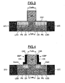
Ceci étant, en variante, en particulier lorsque le matériau utilisé pour la couche intermédiaire est du silicium poreux, on peut laisser subsister sur les flancs de la grille et sur une partie du substrat, une portion de la couche intermédiaire après ladite implantation. On réalise alors des régions latérales isolantes (espaceurs) s'appuyant sur les flancs de la grille et sur une partie du substrat, ces régions latérales isolantes comportant ladite portion résiduelle de couche intermédiaire surmontée d'un autre matériau, par exemple du nitrure de silicium. Les espaceurs finalement réalisés sont alors bi-couches.This being the case, in a variant, in particular when the material used for the intermediate layer is porous silicon, a portion of the intermediate layer may be left on the sidewalls of the gate and on a portion of the substrate after said implantation. We then produces insulating lateral regions (spacers) resting on the sides of the gate and on a portion of the substrate, these insulating lateral regions comprising said residual intermediate layer portion surmounted by another material, for example silicon nitride. The spacers finally made are then two-layered.
On choisit avantageusement l'énergie d'implantation de façon à obtenir un maximum de distribution de dopants à une profondeur d'au moins 3 à 4 nm.The implantation energy is advantageously chosen so as to obtain a maximum of dopant distribution at a depth of at least 3 to 4 nm.
Le fait de s'autoriser, dans le cadre de cette invention, des énergies d'implantation plus élevées, permet de limiter l'impact de la ré-oxydation parasite liée à l'opération de gravure de la couche intermédiaire formée de matériau BARC, puisque la distribution des dopants est située plus loin de la surface ré-oxydée. La consommation de dopants dans l'oxyde reste alors marginale.Authorizing, in the context of this invention, higher implantation energies, makes it possible to limit the impact of the parasite reoxidation associated with the etching operation of the intermediate layer formed of BARC material, since the dopant distribution is located further from the re-oxidized surface. The consumption of dopants in the oxide then remains marginal.
Il convient de noter qu'il est également possible de faire diffuser les dopants, via un recuit thermique d'activation, avant le retrait de la couche intermédiaire, afin de se prémunir de tout effet parasite de surface lié à la gravure ou à tout nettoyage postérieur.It should be noted that it is also possible to cause the dopants to be diffused, via an activation thermal annealing, before the removal of the intermediate layer, in order to guard against any surface parasitic effect associated with etching or any cleaning. posterior.
L'invention a également pour objet un circuit intégré comportant au moins un transistor obtenu par le procédé, tel que défini ci-avant.The invention also relates to an integrated circuit comprising at least one transistor obtained by the method, as defined above.
Selon un mode de réalisation, le transistor comporte des régions latérales isolantes s'appuyant sur les flancs de la grille et sur une partie du substrat, ces régions latérales isolantes comportant une couche intermédiaire formée d'un matériau moins dense que le silicium, par exemple du silicium poreux, cette couche intermédiaire étant surmontée d'un autre matériau.According to one embodiment, the transistor comprises insulating lateral regions resting on the sides of the gate and on a portion of the substrate, these insulating lateral regions comprising an intermediate layer formed of a less dense material than silicon, for example porous silicon, this intermediate layer being surmounted by another material.
D'autres avantages et caractéristiques de l'invention apparaîtront à l'examen de la description détaillée de modes de réalisation et de mise en oeuvre, nullement limitatifs, et des dessins annexés, sur lesquels :
- les
figures 1 à 3 illustrent un premier mode de mise en oeuvre d'un procédé selon l'invention, aboutissant à un premier mode de réalisation d'un transistor selon l'invention ; et - la
figure 4 illustre une variante de l'invention.
- the
Figures 1 to 3 illustrate a first embodiment of a method according to the invention, resulting in a first embodiment of a transistor according to the invention; and - the
figure 4 illustrates a variant of the invention.
Sur les
Ces régions d'isolement latérales STI sont réalisées de façon classique et connue en soi par l'homme du métier.These lateral isolation regions STI are made in a conventional manner and known per se to those skilled in the art.
Après avoir également réalisé de façon classique et connue en soi la grille GR du transistor, isolée de la zone active par un oxyde de grille OX, on dépose une couche intermédiaire CI formée ici d'un matériau de type BARC, en une épaisseur typiquement comprise entre 1 et 100 nm.After having also realized conventionally and known per se the gate GR of the transistor, isolated from the active zone by a gate oxide OX, an intermediate layer CI is deposited here formed of a BARC type material, in a thickness typically comprised between 1 and 100 nm.
Cette couche CI est déposée de manière conforme. Ce matériau inorganique de type BARC présente une très faible densité, typiquement 1 g/cm3.This CI layer is suitably deposited. This inorganic BARC type material has a very low density, typically 1 g / cm 3 .
Puis, on effectue (
Puis, on procède à l'implantation de dopants IMP dans l'orifice délimité par le bloc de résine. Cette implantation IMP se fait ainsi notamment à travers la portion horizontale de la couche CI, de façon à former les régions LDD.Then IMP implantation is carried out in the orifice delimited by the resin block. This implantation IMP is thus done in particular through the horizontal portion of the layer CI, so as to form the LDD regions.
Le décalage latéral, apporté par la partie verticale de la couche CI, est ici supérieur à l'augmentation de la dispersion latérale liée à l'augmentation de l'énergie d'implantation nécessaire à la traversée en profondeur de la couche CI. On obtient donc une longueur électrique Lelec, certes inférieure à la longueur de la grille Lgrille, mais supérieure à celle que l'on aurait obtenue dans le procédé classique de l'art antérieur.The lateral shift, provided by the vertical portion of the IC layer, is here greater than the increase in lateral dispersion related to the increase in the implantation energy necessary for the depth crossing of the IC layer. One thus obtains an electrical length L elec, certainly less than the length L of the gate grid, but greater than that which would have been obtained in the conventional process of the prior art.
En ce qui concerne l'énergie d'implantation, qui doit être un peu plus élevée que celle utilisée dans le procédé de l'art antérieur, en raison de la traversée de la couche CI, l'homme du métier saura la choisir, de façon à obtenir un maximum de distribution des dopants à une profondeur d'au moins 3 à 4 nm, par exemple 10 nm.As regards the implantation energy, which must be a little higher than that used in the process of the prior art, because of the crossing of the layer CI, the person skilled in the art will know how to choose it, from in order to obtain a maximum distribution of the dopants at a depth of at least 3 to 4 nm, for example 10 nm.
A titre indicatif, pour un maximum de distribution à 10 nm avec une implantation à travers 20 nm de couche CI formée de matériau de type BARC, on obtient une dispersion latérale post-implantation sous la grille diminuée d'environ 10 nm par rapport à une implantation à travers une épaisseur équivalente de dioxyde de silicium (densité 2,3 g/cm3) et diminuée d'environ 7 nm par rapport à une implantation classique directe dans du silicium c'est à dire sans espaceurs de décalage.As an indication, for a maximum distribution at 10 nm with implantation through 20 nm of layer CI formed of BARC type material, a lateral dispersion is obtained post-implantation under the reduced gate of about 10 nm compared to a implantation through an equivalent thickness of silicon dioxide (density 2.3 g / cm 3 ) and decreased by about 7 nm compared to a conventional direct implantation in silicon, that is to say without offset spacers.
On procède également, bien que cela ne soit pas absolument indispensable, à la formation, par implantation oblique de dopants de type opposé à celui utilisé pour les implantations de source, drain et LDD, à des régions PK (« pocket » en langue anglaise). L'implantation de ces régions PK peut s'effectuer avant ou après l'implantation des zones LDD. Ces régions PK contribuent à améliorer le contrôle des effets canaux courts et évitent notamment une trop grande chute de la tension de seuil du transistor.There is also, although this is not absolutely essential, the formation, by oblique implantation of dopants of the opposite type to that used for the implantations of source, drain and LDD, PK regions ("pocket" in English) . The implantation of these PK regions can be carried out before or after the implantation of the LDD zones. These PK regions contribute to improving the control of short-channel effects and in particular avoid a too large drop in the threshold voltage of the transistor.
Contrairement à la mise en oeuvre d'espaceurs « offset » selon l'art antérieur, il est possible dans le cadre de la présente invention de réaliser l'implantation des zones PK avec le même niveau de masquage photo-lithographique que celui des zones LDD en préservant leur efficacité. En effet il est connu que l'efficacité de ces poches est reliée à leur localisation précise dans la zone active sous la grille. Cette localisation est d'autant moins dispersée que leur énergie d'implantation est faible. Dans le cas d'espaceurs offset selon l'art antérieur, il est nécessaire d'augmenter significativement l'énergie d'implantation des zones PK. Aussi selon l'art antérieur, il est alors usuel de faire un premier niveau de masquage (avant les espaceurs offset) pour implanter ces zones PK de façon auto-alignée sur la grille, de retirer la résine, de former les espaceurs offset et de refaire un nouveau niveau de masquage pour les zones LDD.Unlike the implementation of "offset" spacers according to the prior art, it is possible in the context of the present invention to implement the PK zones with the same level of photo-lithographic masking as that of the LDD zones. preserving their effectiveness. Indeed it is known that the effectiveness of these pockets is related to their precise location in the active area under the grid. This location is even less dispersed as their implantation energy is low. In the case of offset spacers according to the prior art, it is necessary to significantly increase the implantation energy of the PK zones. Also according to the prior art, it is then customary to make a first level of masking (before the offset spacers) to implant these PK zones in a self-aligned manner on the grid, to remove the resin, to form the offset spacers and to redo a new level of masking for LDD zones.
Dans le cadre de la présente invention, il est possible de s'affranchir de cette coûteuse limitation puisque la densité des matériaux utilisés est faible, et que par conséquent l'augmentation d'énergie pour implanter les poches PK à travers la couche intermédiaire est tout à fait acceptable.In the context of the present invention, it is possible to overcome this costly limitation since the density of the materials used is low, and therefore the increase energy to implant the PK bags through the intermediate layer is quite acceptable.
L'étape suivante consiste à retirer par gravure sous plasma contenant de l'oxygène, la couche CI (
Le type de gravure permettant le retrait de la couche CI est oxydant et conduit à la formation d'un oxyde de surface OX1.The type of etching for the removal of the IC layer is oxidizing and leads to the formation of a surface oxide OX1.
Le fait de s'autoriser, dans le cadre de cette invention, une énergie d'implantation plus élevée, permet de limiter l'impact de la ré-oxydation parasite OX1 liée à la gravure du matériau BARC, puisque la distribution de dopants est située plus loin de la surface ré-oxydée. La consommation de dopants dans l'oxyde reste alors marginale.The fact of being authorized, in the context of this invention, a higher implantation energy, makes it possible to limit the impact of the parasite reoxidation OX1 related to the etching of the BARC material, since the distribution of dopants is located further from the re-oxidized surface. The consumption of dopants in the oxide then remains marginal.
Par ailleurs, selon une variante de l'invention, on peut procéder à l'implantation des zones PK après retrait de la couche CI et avant retrait de la résine. Une telle variante permet d'implanter les zones PK de façon auto-alignée sur la grille tout en décalant l'implantation des zones LDD pour contrôler les effets canaux courts et cela avec le même niveau photolithographique.Moreover, according to a variant of the invention, it is possible to proceed with the implantation of the PK zones after removal of the IC layer and before removal of the resin. Such a variant makes it possible to implant the PK zones in a self-aligned manner on the grid while shifting the implantation of the LDD zones to control the short channel effects and that with the same photolithographic level.
Le reste du procédé de fabrication du transistor est classique et connu en soi et comporte notamment le retrait de la couche OX1, puis la formation d'espaceurs isolants, par exemple en nitrure de silicium, sur les flancs de la grille.The remainder of the method of manufacturing the transistor is conventional and known per se and comprises in particular the removal of the layer OX1, then the formation of insulating spacers, for example silicon nitride, on the sides of the gate.
L'invention n'est pas limitée aux modes de réalisation et de mise en oeuvre qui viennent d'être décrits, mais en embrasse toutes les variantes.The invention is not limited to the embodiments and implementations which have just been described, but encompasses all the variants.
Ainsi, le matériau de type BARC peut être remplacé par tout matériau de faible densité (inférieur au dioxyde de silicium) et capable d'être gravé sélectivement par rapport au silicium.Thus, the BARC type material can be replaced by any low density material (less than silicon dioxide) and capable of being etched selectively with respect to silicon.
A titre d'exemple, on peut citer du dioxyde de silicium poreux. Un tel matériau présente également l'avantage de ne pas modifier significativement le procédé de fabrication classique d'un transistor MOS.By way of example, mention may be made of porous silicon dioxide. Such a material also has the advantage of not significantly modifying the conventional manufacturing method of a MOS transistor.
En effet, comme illustré sur la
Claims (9)
- Process for fabricating a MOS transistor, comprising a step of producing source and drain extension regions, consisting in forming a gate region on a semiconductor substrate and in implanting dopants into the substrate on either side of and at a certain distance from the gate of the transistor, said step of producing the source and drain extension regions consists in forming an intermediate layer (CI) on the sidewalls of the gate (GR) and on the surface of the substrate and said implantation of dopants (IMP) is carried out through that part of said intermediate layer which is located on the substrate, characterized in that this intermediate layer is formed from a material that is less dense than silicon dioxide.
- Process according to Claim 1, characterized in that the material forming the intermediate layer (CI) is an antireflective material used as antireflective sublayer during exposure of a photoresist.
- Process according to Claim 1, characterized in that the material forming the intermediate layer (CI) is porous silicon dioxide.
- Process according to one of the preceding claims, characterized in that pockets (PK) are formed by oblique implantation of dopants of the opposite type to that used for the source, drain and source and drain extension region (LDD) implantations and in that this oblique implantation is carried out through the intermediate layer.
- Process according to one of the preceding claims, characterized in that the material forming the intermediate layer (CI) may be etched selectively with respect to silicon and in that said intermediate layer is removed after said implantation of dopants.
- Process according to Claim 5, characterized in that pockets (PK) are formed by oblique implantation of dopants of the opposite type to that used for the source, drain and source and drain extension region (LDD) implantations and in that this oblique implantation is carried out after the intermediate layer has been removed.
- Process according to Claim 3, characterized in that, after said implantation, a portion (CIR) of the intermediate layer is left to remain on the sidewalls of the gate (GR) and on part of the substrate and in that insulating lateral regions resting on the sidewalls of the gate and on part of the substrate are produced, these insulating lateral regions (ESP) comprising said residual portion of the intermediate layer surmounted by another material.
- Process according to one of the preceding claims, characterized in that the implantation energy is chosen so as to obtain a maximum dopant distribution at a depth of at least 3 to 4 nanometres.
- Process according to one of the preceding claims, characterized in that the length of the gate measured parallel to the length of the channel is less than 180 nanometres, for example less than 100 nanometres.
Applications Claiming Priority (2)
| Application Number | Priority Date | Filing Date | Title |
|---|---|---|---|
| FR0206870 | 2002-06-04 | ||
| FR0206870A FR2840453B1 (en) | 2002-06-04 | 2002-06-04 | METHOD FOR MANUFACTURING A MOS TRANSISTOR OF REDUCED GRID LENGTH, AND INTEGRATED CIRCUIT COMPRISING SUCH A TRANSISTOR |
Publications (2)
| Publication Number | Publication Date |
|---|---|
| EP1369909A1 EP1369909A1 (en) | 2003-12-10 |
| EP1369909B1 true EP1369909B1 (en) | 2011-02-02 |
Family
ID=29433315
Family Applications (1)
| Application Number | Title | Priority Date | Filing Date |
|---|---|---|---|
| EP03291262A Expired - Lifetime EP1369909B1 (en) | 2002-06-04 | 2003-05-27 | Method of fabricating a MOS transistor with reduced gate length and integrated circuit comprising such transistor |
Country Status (4)
| Country | Link |
|---|---|
| US (1) | US6806156B2 (en) |
| EP (1) | EP1369909B1 (en) |
| DE (1) | DE60335930D1 (en) |
| FR (1) | FR2840453B1 (en) |
Families Citing this family (5)
| Publication number | Priority date | Publication date | Assignee | Title |
|---|---|---|---|---|
| KR100468785B1 (en) * | 2003-02-19 | 2005-01-29 | 삼성전자주식회사 | Method of fabricating MOS Field Effect Transistor with pocket region |
| US7420233B2 (en) * | 2003-10-22 | 2008-09-02 | Micron Technology, Inc. | Photodiode for improved transfer gate leakage |
| US7585763B2 (en) * | 2005-11-07 | 2009-09-08 | Samsung Electronics Co., Ltd. | Methods of fabricating integrated circuit devices using anti-reflective coating as implant blocking layer |
| US9530864B2 (en) * | 2014-06-25 | 2016-12-27 | Globalfoundries Inc. | Junction overlap control in a semiconductor device using a sacrificial spacer layer |
| CN113871451B (en) * | 2021-09-24 | 2024-06-18 | 华虹半导体(无锡)有限公司 | DMOS device and forming method thereof |
Family Cites Families (13)
| Publication number | Priority date | Publication date | Assignee | Title |
|---|---|---|---|---|
| US5492847A (en) * | 1994-08-01 | 1996-02-20 | National Semiconductor Corporation | Counter-implantation method of manufacturing a semiconductor device with self-aligned anti-punchthrough pockets |
| US5976769A (en) * | 1995-07-14 | 1999-11-02 | Texas Instruments Incorporated | Intermediate layer lithography |
| US5736446A (en) * | 1997-05-21 | 1998-04-07 | Powerchip Semiconductor Corp. | Method of fabricating a MOS device having a gate-side air-gap structure |
| US6180472B1 (en) * | 1998-07-28 | 2001-01-30 | Matsushita Electrons Corporation | Method for fabricating semiconductor device |
| US6274445B1 (en) * | 1999-02-03 | 2001-08-14 | Philips Semi-Conductor, Inc. | Method of manufacturing shallow source/drain junctions in a salicide process |
| US6274426B1 (en) * | 1999-02-25 | 2001-08-14 | Taiwan Semiconductor Manufacturing Company | Self-aligned contact process for a crown shaped dynamic random access memory capacitor structure |
| GB2362029A (en) * | 1999-10-27 | 2001-11-07 | Lucent Technologies Inc | Multi-layer structure for MOSFET Spacers |
| US6277683B1 (en) * | 2000-02-28 | 2001-08-21 | Chartered Semiconductor Manufacturing Ltd. | Method of forming a sidewall spacer and a salicide blocking shape, using only one silicon nitride layer |
| US6642590B1 (en) * | 2000-10-19 | 2003-11-04 | Advanced Micro Devices, Inc. | Metal gate with PVD amorphous silicon layer and barrier layer for CMOS devices and method of making with a replacement gate process |
| US6664143B2 (en) * | 2000-11-22 | 2003-12-16 | North Carolina State University | Methods of fabricating vertical field effect transistors by conformal channel layer deposition on sidewalls |
| US6537860B2 (en) * | 2000-12-18 | 2003-03-25 | Apd Semiconductor, Inc. | Method of fabricating power VLSI diode devices |
| US6448165B1 (en) * | 2000-12-21 | 2002-09-10 | Advanced Micro Devices, Inc. | Method for controlling the amount of trim of a gate structure of a field effect transistor |
| US6727534B1 (en) * | 2001-12-20 | 2004-04-27 | Advanced Micro Devices, Inc. | Electrically programmed MOS transistor source/drain series resistance |
-
2002
- 2002-06-04 FR FR0206870A patent/FR2840453B1/en not_active Expired - Fee Related
-
2003
- 2003-05-27 EP EP03291262A patent/EP1369909B1/en not_active Expired - Lifetime
- 2003-05-27 DE DE60335930T patent/DE60335930D1/en not_active Expired - Lifetime
- 2003-06-04 US US10/454,361 patent/US6806156B2/en not_active Expired - Lifetime
Also Published As
| Publication number | Publication date |
|---|---|
| US20040046192A1 (en) | 2004-03-11 |
| US6806156B2 (en) | 2004-10-19 |
| FR2840453A1 (en) | 2003-12-05 |
| DE60335930D1 (en) | 2011-03-17 |
| FR2840453B1 (en) | 2005-06-24 |
| EP1369909A1 (en) | 2003-12-10 |
Similar Documents
| Publication | Publication Date | Title |
|---|---|---|
| EP0426251A1 (en) | Process for manufacturing a device having MIS transistors with an inverted T-shaped gate electrode | |
| US6927130B2 (en) | Method of manufacturing a trench gate type field effect transistor | |
| EP1959481B1 (en) | Method of manufacturing a transistor | |
| FR2806832A1 (en) | METAL SOURCE AND DRAIN MOS TRANSISTOR, AND METHOD FOR MANUFACTURING SUCH A TRANSISTOR | |
| FR3060850A1 (en) | PROCESS FOR MANUFACTURING A VERTICAL CHANNEL NANOCOUCHES TRANSISTOR | |
| FR3043837A1 (en) | METHOD FOR PRODUCING A SEMICONDUCTOR NANOFIL TRANSISTOR COMPRISING A SELF-ALIGNED GRID AND SPACERS | |
| EP2610915A1 (en) | Transistor and method for manufacturing a transistor | |
| US20050009278A1 (en) | Methods of fabricating multiple sets of field effect transistors | |
| WO2014037411A1 (en) | Process for producing fet transistors | |
| EP1369909B1 (en) | Method of fabricating a MOS transistor with reduced gate length and integrated circuit comprising such transistor | |
| FR3036530A1 (en) | METHOD FOR MAKING SINGLE PROGRAMMING MEMORY CELLS COMPRISING MOS CAPACITORS AND CORRESPONDING INTEGRATED CIRCUIT | |
| FR2847383A1 (en) | Fabrication of an integrated circuit incorporating a MOSFET with a reduced gate length | |
| US6664153B2 (en) | Method to fabricate a single gate with dual work-functions | |
| EP2120258A1 (en) | Method for manufacturing a transistor with metal source and drain | |
| FR3067516A1 (en) | IMPLEMENTING SEMICONDUCTOR REGIONS IN AN ELECTRONIC CHIP | |
| EP2569801A1 (en) | Process for producing a conducting electrode | |
| JP4782411B2 (en) | Semiconductor device and manufacturing method thereof | |
| US20050245015A1 (en) | Method for manufacturing a semiconductor device having a dual-gate structure | |
| EP3490007A1 (en) | Method for manufacturing fin-fet type cmos transistor pairs at low temperature | |
| EP0522938B1 (en) | Method for fabrication of a vertical field effect transistor and transistor obtained by this method | |
| EP1328969B1 (en) | Method of manufacturing a mos transistor | |
| EP3065180B1 (en) | Transistor with mis connections and manufacturing method | |
| WO2006070154A1 (en) | Improved semiconductor thin-film transistor structure | |
| EP0607075B1 (en) | Semiconductor electronic component having a negative dynamic resistance and corresponding using methods and manufacturing process | |
| EP2479785A1 (en) | Field-effect device provided with a barrier zone for localised dopant scattering and manufacturing method |
Legal Events
| Date | Code | Title | Description |
|---|---|---|---|
| PUAI | Public reference made under article 153(3) epc to a published international application that has entered the european phase |
Free format text: ORIGINAL CODE: 0009012 |
|
| AK | Designated contracting states |
Kind code of ref document: A1 Designated state(s): AT BE BG CH CY CZ DE DK EE ES FI FR GB GR HU IE IT LI LU MC NL PT RO SE SI SK TR |
|
| AX | Request for extension of the european patent |
Extension state: AL LT LV MK |
|
| 17P | Request for examination filed |
Effective date: 20040609 |
|
| AKX | Designation fees paid |
Designated state(s): DE FR GB IT |
|
| 17Q | First examination report despatched |
Effective date: 20100219 |
|
| RAP1 | Party data changed (applicant data changed or rights of an application transferred) |
Owner name: STMICROELECTRONICS S.A. Owner name: COMMISSARIAT A L'ENERGIE ATOMIQUE ET AUX ENERGIES |
|
| GRAP | Despatch of communication of intention to grant a patent |
Free format text: ORIGINAL CODE: EPIDOSNIGR1 |
|
| GRAS | Grant fee paid |
Free format text: ORIGINAL CODE: EPIDOSNIGR3 |
|
| GRAA | (expected) grant |
Free format text: ORIGINAL CODE: 0009210 |
|
| AK | Designated contracting states |
Kind code of ref document: B1 Designated state(s): DE FR GB IT |
|
| REG | Reference to a national code |
Ref country code: GB Ref legal event code: FG4D Free format text: NOT ENGLISH |
|
| REF | Corresponds to: |
Ref document number: 60335930 Country of ref document: DE Date of ref document: 20110317 Kind code of ref document: P |
|
| REG | Reference to a national code |
Ref country code: DE Ref legal event code: R096 Ref document number: 60335930 Country of ref document: DE Effective date: 20110317 |
|
| PLBE | No opposition filed within time limit |
Free format text: ORIGINAL CODE: 0009261 |
|
| STAA | Information on the status of an ep patent application or granted ep patent |
Free format text: STATUS: NO OPPOSITION FILED WITHIN TIME LIMIT |
|
| 26N | No opposition filed |
Effective date: 20111103 |
|
| REG | Reference to a national code |
Ref country code: DE Ref legal event code: R097 Ref document number: 60335930 Country of ref document: DE Effective date: 20111103 |
|
| PGFP | Annual fee paid to national office [announced via postgrant information from national office to epo] |
Ref country code: DE Payment date: 20120423 Year of fee payment: 10 |
|
| PGFP | Annual fee paid to national office [announced via postgrant information from national office to epo] |
Ref country code: FR Payment date: 20120625 Year of fee payment: 10 Ref country code: GB Payment date: 20120423 Year of fee payment: 10 |
|
| PGFP | Annual fee paid to national office [announced via postgrant information from national office to epo] |
Ref country code: IT Payment date: 20120421 Year of fee payment: 10 |
|
| GBPC | Gb: european patent ceased through non-payment of renewal fee |
Effective date: 20130527 |
|
| PG25 | Lapsed in a contracting state [announced via postgrant information from national office to epo] |
Ref country code: DE Free format text: LAPSE BECAUSE OF NON-PAYMENT OF DUE FEES Effective date: 20131203 |
|
| PG25 | Lapsed in a contracting state [announced via postgrant information from national office to epo] |
Ref country code: IT Free format text: LAPSE BECAUSE OF NON-PAYMENT OF DUE FEES Effective date: 20130527 |
|
| REG | Reference to a national code |
Ref country code: DE Ref legal event code: R119 Ref document number: 60335930 Country of ref document: DE Effective date: 20131203 |
|
| REG | Reference to a national code |
Ref country code: FR Ref legal event code: ST Effective date: 20140131 |
|
| PG25 | Lapsed in a contracting state [announced via postgrant information from national office to epo] |
Ref country code: GB Free format text: LAPSE BECAUSE OF NON-PAYMENT OF DUE FEES Effective date: 20130527 |
|
| PG25 | Lapsed in a contracting state [announced via postgrant information from national office to epo] |
Ref country code: FR Free format text: LAPSE BECAUSE OF NON-PAYMENT OF DUE FEES Effective date: 20130531 |