EP1369828A2 - Personalisiertes digitales Datenbearbeitungssystem - Google Patents
Personalisiertes digitales Datenbearbeitungssystem Download PDFInfo
- Publication number
- EP1369828A2 EP1369828A2 EP03012159A EP03012159A EP1369828A2 EP 1369828 A2 EP1369828 A2 EP 1369828A2 EP 03012159 A EP03012159 A EP 03012159A EP 03012159 A EP03012159 A EP 03012159A EP 1369828 A2 EP1369828 A2 EP 1369828A2
- Authority
- EP
- European Patent Office
- Prior art keywords
- memory
- data processing
- processing system
- digital data
- write
- Prior art date
- Legal status (The legal status is an assumption and is not a legal conclusion. Google has not performed a legal analysis and makes no representation as to the accuracy of the status listed.)
- Withdrawn
Links
Images


Classifications
-
- G—PHYSICS
- G07—CHECKING-DEVICES
- G07F—COIN-FREED OR LIKE APPARATUS
- G07F7/00—Mechanisms actuated by objects other than coins to free or to actuate vending, hiring, coin or paper currency dispensing or refunding apparatus
- G07F7/08—Mechanisms actuated by objects other than coins to free or to actuate vending, hiring, coin or paper currency dispensing or refunding apparatus by coded identity card or credit card or other personal identification means
- G07F7/10—Mechanisms actuated by objects other than coins to free or to actuate vending, hiring, coin or paper currency dispensing or refunding apparatus by coded identity card or credit card or other personal identification means together with a coded signal, e.g. in the form of personal identification information, like personal identification number [PIN] or biometric data
- G07F7/1008—Active credit-cards provided with means to personalise their use, e.g. with PIN-introduction/comparison system
-
- G—PHYSICS
- G06—COMPUTING OR CALCULATING; COUNTING
- G06F—ELECTRIC DIGITAL DATA PROCESSING
- G06F21/00—Security arrangements for protecting computers, components thereof, programs or data against unauthorised activity
- G06F21/70—Protecting specific internal or peripheral components, in which the protection of a component leads to protection of the entire computer
- G06F21/78—Protecting specific internal or peripheral components, in which the protection of a component leads to protection of the entire computer to assure secure storage of data
-
- G—PHYSICS
- G06—COMPUTING OR CALCULATING; COUNTING
- G06Q—INFORMATION AND COMMUNICATION TECHNOLOGY [ICT] SPECIALLY ADAPTED FOR ADMINISTRATIVE, COMMERCIAL, FINANCIAL, MANAGERIAL OR SUPERVISORY PURPOSES; SYSTEMS OR METHODS SPECIALLY ADAPTED FOR ADMINISTRATIVE, COMMERCIAL, FINANCIAL, MANAGERIAL OR SUPERVISORY PURPOSES, NOT OTHERWISE PROVIDED FOR
- G06Q20/00—Payment architectures, schemes or protocols
- G06Q20/30—Payment architectures, schemes or protocols characterised by the use of specific devices or networks
- G06Q20/34—Payment architectures, schemes or protocols characterised by the use of specific devices or networks using cards, e.g. integrated circuit [IC] cards or magnetic cards
- G06Q20/341—Active cards, i.e. cards including their own processing means, e.g. including an IC or chip
-
- G—PHYSICS
- G06—COMPUTING OR CALCULATING; COUNTING
- G06Q—INFORMATION AND COMMUNICATION TECHNOLOGY [ICT] SPECIALLY ADAPTED FOR ADMINISTRATIVE, COMMERCIAL, FINANCIAL, MANAGERIAL OR SUPERVISORY PURPOSES; SYSTEMS OR METHODS SPECIALLY ADAPTED FOR ADMINISTRATIVE, COMMERCIAL, FINANCIAL, MANAGERIAL OR SUPERVISORY PURPOSES, NOT OTHERWISE PROVIDED FOR
- G06Q20/00—Payment architectures, schemes or protocols
- G06Q20/30—Payment architectures, schemes or protocols characterised by the use of specific devices or networks
- G06Q20/34—Payment architectures, schemes or protocols characterised by the use of specific devices or networks using cards, e.g. integrated circuit [IC] cards or magnetic cards
- G06Q20/355—Personalisation of cards for use
- G06Q20/3552—Downloading or loading of personalisation data
-
- G—PHYSICS
- G06—COMPUTING OR CALCULATING; COUNTING
- G06Q—INFORMATION AND COMMUNICATION TECHNOLOGY [ICT] SPECIALLY ADAPTED FOR ADMINISTRATIVE, COMMERCIAL, FINANCIAL, MANAGERIAL OR SUPERVISORY PURPOSES; SYSTEMS OR METHODS SPECIALLY ADAPTED FOR ADMINISTRATIVE, COMMERCIAL, FINANCIAL, MANAGERIAL OR SUPERVISORY PURPOSES, NOT OTHERWISE PROVIDED FOR
- G06Q20/00—Payment architectures, schemes or protocols
- G06Q20/30—Payment architectures, schemes or protocols characterised by the use of specific devices or networks
- G06Q20/34—Payment architectures, schemes or protocols characterised by the use of specific devices or networks using cards, e.g. integrated circuit [IC] cards or magnetic cards
- G06Q20/357—Cards having a plurality of specified features
- G06Q20/3576—Multiple memory zones on card
- G06Q20/35765—Access rights to memory zones
Definitions
- the present invention relates to a method of personalising a digital data processing system and to a personalised digital data processing system.
- a digital data processing system When a digital data processing system is intended to be exclusively used with a specific application or by particular user, it can be linked to the specific application or particular user by introducing some "personalising" information that must not thereafter be overwritten. The user or application linked to the system would then need to present to the system some matching data such as a PIN code to be entered with a keypad or a particular code read from a chip-card in order to enable operation of the system.
- the personalising data are stored in a one-time programmable, non-volatile memory that is either embedded within the system or is a separate component associated with the system in a common package. Fuse technologies are available for one-time programming of a non-volatile memory.
- ASIC Application Specific Integrated Circuit
- the present invention provides a way to use a usual non-volatile read-write memory as a one-time programmable memory.
- the invention provides a method of personalising a digital data processing system that contains a non-volatile memory, by writing personalising data into the memory. Initially, a predetermined write authorisation bits pattern is written into at least an area of the blank memory. After the reset of the digital data processing, the contents of that memory area are accessed and read. The memory contents thus read are then compared with the predetermined write authorisation bits pattern. If, and only if, they match, a write operation in the memory area is permitted, and personalising data can be written in the memory area. Otherwise the write request is rejected.
- the invention also provides a digital data processing system containing a core processing component and a non-volatile memory within a single package.
- the non-volatile memory includes either a predetermined write authorisation bits pattern or personalising data. If the write authorisation bits pattern is found in the memory, it may be overwritten with personalising data. If the write authorisation bits pattern is not found, any write request will be rejected during all the session.
- the non-volatile memory is in fact a one-time programmable memory.
- a digital data processing system is materialised in a multi-chip ASIC module.
- the ASIC module 10 may be a secured processor embedded in a CAM (Conditional Access Module) for use in a DVB (Digital Video Broadcast) environment or embedded in a Smart Card reader for electronic payment application, includes a core processing chip 12 and a non-volatile memory chip14 within a common package. Removal of the memory chip from the package is either destructive to the entire system or at least an operation too costly for misuse on a large scale.
- the core processing chip 12 includes a memory controller 16 for read-write access to memory chip 14.
- a predetermined write authorisation bits pattern is first written into a blank memory chip before the memory chip 14 is combined with the core processing chip 12 into ASIC module 10. Thereafter, any read or write access to memory chip 14 is possible via memory controller 16, only.
- the predetermined write authorisation bits pattern may occupy the entire space of memory chip 14, or only a limited area thereof, preferably from the beginning of memory address space.
- a basic functionality of memory controller 16 is to check the presence of the write authorisation bits pattern in memory chip 14 after each reset of the ASIC module 10 and to reject the write request when the bits pattern is not found as expected. After anything different from the predetermined bits pattern has been written into memory 14, any write requests will be rejected.
- memory 14 (or an area thereof) is a one-time programmable memory, although it may be embodied in a usual non-volatile memory technology.
- the system has an Hardware controller that includes a write authorisation check procedure performed at each reset or boot-up of the system.
- the chip can be personalised and the personalising data are written into memory chip 14 via memory controller 16.
- the system is considered to be personalised, and the system may execute a particular application, possibly subject to a successful identification of the particular user or of a specific application in relation to the personalising data.
- replacing the Hardware controller of the preferred embodiement is an operating system that would perform the write access authorization check procedure.
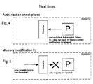
- the predetermined write authorisation bits pattern "A" has been written into memory 14, as confirmed by memory controller 16 in a write authorisation phase.
- memory 14 is a blank memory, and the predetermined write authorisation bits pattern will not be found in memory 14, as illustrated in Fig. 6. Any subsequent write request will be rejected, as illustrated in Fig. 7.
- the predetermined write authorisation bits pattern may occupy the entire memory 14 or only an area thereof. The only requirement is that memory controller 16 must know where to seek for it.
- the personalising data may occupy the entire memory 14 or only an area thereof.
- the write authorisation bits pattern is at least altered, and any subsequent write request will be rejected.
- the size of the one-time programmable memory area is included in the personalising data, such as in the data "P" of Fig. 3.
- the size of that memory area is written at the beginning of the address space of memory 14.
- the write authorisation pattern contains a one-time programmable memory area size of a default value, which is the size of the entire memory. After the memory contents have been read for the first time in a write authorisation check procedure, and the personalising data "P" are written, they will occupy the entire memory size since this is the default value. However, within the personalising data "P", a new (smaller) size of the one-time programmable memory area is included and is preferably written at the beginning of the memory address space.
- the size of the one-time programmable memory area is read first. Then, the write authorisation check is performed on the memory area defined by the one time programmable size. If write access is not allowed, all write access at addresses being in the range of addresses defined by the one-time programable size is rejected.
- a protected mechanism for initially writing the write authorisation bits pattern into the blank memory is provided.
- memory 14 is a discrete memory component.
- the memory component and all other components of the system are packaged in a manner such that removal of the memory component is at least difficult, and preferably destructive to the entire system.
Landscapes
- Engineering & Computer Science (AREA)
- Business, Economics & Management (AREA)
- Physics & Mathematics (AREA)
- General Physics & Mathematics (AREA)
- Theoretical Computer Science (AREA)
- Computer Networks & Wireless Communication (AREA)
- Accounting & Taxation (AREA)
- Strategic Management (AREA)
- Microelectronics & Electronic Packaging (AREA)
- General Business, Economics & Management (AREA)
- Computer Security & Cryptography (AREA)
- Computer Hardware Design (AREA)
- Software Systems (AREA)
- General Engineering & Computer Science (AREA)
- Storage Device Security (AREA)
Applications Claiming Priority (2)
| Application Number | Priority Date | Filing Date | Title |
|---|---|---|---|
| DE10224767A DE10224767A1 (de) | 2002-06-04 | 2002-06-04 | Personalisiertes digitales Datenverarbeitungssystem |
| DE10224767 | 2002-06-04 |
Publications (2)
| Publication Number | Publication Date |
|---|---|
| EP1369828A2 true EP1369828A2 (de) | 2003-12-10 |
| EP1369828A3 EP1369828A3 (de) | 2004-03-10 |
Family
ID=29432630
Family Applications (1)
| Application Number | Title | Priority Date | Filing Date |
|---|---|---|---|
| EP03012159A Withdrawn EP1369828A3 (de) | 2002-06-04 | 2003-06-03 | Personalisiertes digitales Datenbearbeitungssystem |
Country Status (3)
| Country | Link |
|---|---|
| US (1) | US20040044867A1 (de) |
| EP (1) | EP1369828A3 (de) |
| DE (1) | DE10224767A1 (de) |
Cited By (1)
| Publication number | Priority date | Publication date | Assignee | Title |
|---|---|---|---|---|
| EP1971934A1 (de) * | 2005-09-15 | 2008-09-24 | Microchip Technology Incorporated | Programmierung eines digitalen prozessors mit einer einzigen verbindung |
Families Citing this family (3)
| Publication number | Priority date | Publication date | Assignee | Title |
|---|---|---|---|---|
| DE102006022584A1 (de) * | 2006-05-15 | 2007-11-22 | Siemens Ag | Zugangsvorrichtung und Verfahren zum Betreiben derselben |
| TW201104433A (en) * | 2009-07-28 | 2011-02-01 | Jmicron Technology Corp | Communicating method applied for storage device |
| US11436160B2 (en) | 2019-10-03 | 2022-09-06 | Microsoft Technology Licensing, Llc | Protection of data in memory of an integrated circuit using a secret token |
Family Cites Families (11)
| Publication number | Priority date | Publication date | Assignee | Title |
|---|---|---|---|---|
| JPH0632102B2 (ja) * | 1985-08-22 | 1994-04-27 | カシオ計算機株式会社 | Icカ−ドの照合方式 |
| FR2591008B1 (fr) * | 1985-11-30 | 1991-05-17 | Toshiba Kk | Dispositif electronique portatif |
| GB2206431B (en) * | 1987-06-30 | 1991-05-29 | Motorola Inc | Data card circuits |
| US5083293A (en) * | 1989-01-12 | 1992-01-21 | General Instrument Corporation | Prevention of alteration of data stored in secure integrated circuit chip memory |
| JPH0452890A (ja) * | 1990-06-15 | 1992-02-20 | Mitsubishi Electric Corp | Icカード |
| US5974513A (en) * | 1993-11-04 | 1999-10-26 | Hitachi Maxell, Ltd. | IC memory card having read/write inhibit capabilities |
| JPH0844628A (ja) * | 1994-08-03 | 1996-02-16 | Hitachi Ltd | 不揮発性メモリ、およびそれを用いたメモリカード、情報処理装置、ならびに不揮発性メモリのソフトウェアライトプロテクト制御方法 |
| US5864664A (en) * | 1996-08-30 | 1999-01-26 | International Business Machines Corporation | Apparatus and method for protecting system serial number while allowing motherboard replacement |
| FR2770327B1 (fr) * | 1997-10-24 | 2000-01-14 | Sgs Thomson Microelectronics | Memoire non volatile programmable et effacable electriquement comprenant une zone protegeable en lecture et/ou en ecriture et systeme electronique l'incorporant |
| US6304948B1 (en) * | 1998-10-06 | 2001-10-16 | Ricoh Corporation | Method and apparatus for erasing data after expiration |
| JP4678083B2 (ja) * | 2000-09-29 | 2011-04-27 | ソニー株式会社 | メモリ装置およびメモリアクセス制限方法 |
-
2002
- 2002-06-04 DE DE10224767A patent/DE10224767A1/de not_active Withdrawn
-
2003
- 2003-06-03 US US10/452,581 patent/US20040044867A1/en not_active Abandoned
- 2003-06-03 EP EP03012159A patent/EP1369828A3/de not_active Withdrawn
Cited By (1)
| Publication number | Priority date | Publication date | Assignee | Title |
|---|---|---|---|---|
| EP1971934A1 (de) * | 2005-09-15 | 2008-09-24 | Microchip Technology Incorporated | Programmierung eines digitalen prozessors mit einer einzigen verbindung |
Also Published As
| Publication number | Publication date |
|---|---|
| US20040044867A1 (en) | 2004-03-04 |
| DE10224767A1 (de) | 2003-12-18 |
| EP1369828A3 (de) | 2004-03-10 |
Similar Documents
| Publication | Publication Date | Title |
|---|---|---|
| US7281101B2 (en) | Memory device storing data relating to specific application programs | |
| JPH06259248A (ja) | メモリカード | |
| US9250930B2 (en) | Configuration method for an electronic entity | |
| KR940007351B1 (ko) | 휴대가능 전자장치 | |
| JP2005515542A (ja) | 対応するコンピュータプログラム及び対応するコンピュータにより読み出し可能な記憶媒体と共にコントローラアーキテクチャにおけるnvメモリに書き込むための装置及び方法 | |
| JP2013535748A (ja) | 電子チケット記憶装置、電子チケット確認システム及び方法 | |
| US6766961B2 (en) | IC card | |
| US6779732B2 (en) | Method and apparatus for linking converted applet files | |
| US20050259465A1 (en) | Nonvolatile memory apparatus | |
| US20080005799A1 (en) | Program execution control circuit, computer system, and IC card | |
| EP1369828A2 (de) | Personalisiertes digitales Datenbearbeitungssystem | |
| US20240273206A1 (en) | Personalization of a secure element | |
| JPH04264688A (ja) | メモリカードの暗証コードを承認する方法 | |
| WO2007107829A2 (en) | A personal security token for at least two security environments and different access conditions thereupon | |
| US7014119B2 (en) | Method of manufacturing smart cards | |
| US20100057980A1 (en) | Data memory device with auxiliary function | |
| US12596539B2 (en) | Hiding and unhiding java card applet instances | |
| AU2002254795B2 (en) | Method of manufacturing smart cards | |
| US20070043993A1 (en) | System and method for protection of data contained in an integrated circuit | |
| KR20120017790A (ko) | 운영체제의 재쓰기 가능한 메모리 영역을 갖는 스마트카드 및 그 운용방법 | |
| JP2006293706A (ja) | アプリケーションの更新機能を有するマルチアプリケーションicカード | |
| JP2000163546A (ja) | Icカード及びその使用方法 | |
| US20100200650A1 (en) | Mobile communication device and method for recovering mifare memory | |
| KR20040034782A (ko) | 스마트 카드를 이용한 단말기 시스템 업그레이드 방법 및그 장치 | |
| AU2002254795A1 (en) | Method of manufacturing smart cards |
Legal Events
| Date | Code | Title | Description |
|---|---|---|---|
| PUAI | Public reference made under article 153(3) epc to a published international application that has entered the european phase |
Free format text: ORIGINAL CODE: 0009012 |
|
| AK | Designated contracting states |
Kind code of ref document: A2 Designated state(s): AT BE BG CH CY CZ DE DK EE ES FI FR GB GR HU IE IT LI LU MC NL PT RO SE SI SK TR |
|
| AX | Request for extension of the european patent |
Extension state: AL LT LV MK |
|
| PUAL | Search report despatched |
Free format text: ORIGINAL CODE: 0009013 |
|
| AK | Designated contracting states |
Kind code of ref document: A3 Designated state(s): AT BE BG CH CY CZ DE DK EE ES FI FR GB GR HU IE IT LI LU MC NL PT RO SE SI SK TR |
|
| AX | Request for extension of the european patent |
Extension state: AL LT LV MK |
|
| AKX | Designation fees paid | ||
| REG | Reference to a national code |
Ref country code: DE Ref legal event code: 8566 |
|
| STAA | Information on the status of an ep patent application or granted ep patent |
Free format text: STATUS: THE APPLICATION IS DEEMED TO BE WITHDRAWN |
|
| 18D | Application deemed to be withdrawn |
Effective date: 20040911 |