EP1365637A2 - Copper circuit formed by kinetic spray - Google Patents
Copper circuit formed by kinetic spray Download PDFInfo
- Publication number
- EP1365637A2 EP1365637A2 EP03076330A EP03076330A EP1365637A2 EP 1365637 A2 EP1365637 A2 EP 1365637A2 EP 03076330 A EP03076330 A EP 03076330A EP 03076330 A EP03076330 A EP 03076330A EP 1365637 A2 EP1365637 A2 EP 1365637A2
- Authority
- EP
- European Patent Office
- Prior art keywords
- copper
- substrate
- bond layer
- particles
- silver
- Prior art date
- Legal status (The legal status is an assumption and is not a legal conclusion. Google has not performed a legal analysis and makes no representation as to the accuracy of the status listed.)
- Withdrawn
Links
Images


Classifications
-
- H—ELECTRICITY
- H05—ELECTRIC TECHNIQUES NOT OTHERWISE PROVIDED FOR
- H05K—PRINTED CIRCUITS; CASINGS OR CONSTRUCTIONAL DETAILS OF ELECTRIC APPARATUS; MANUFACTURE OF ASSEMBLAGES OF ELECTRICAL COMPONENTS
- H05K3/00—Apparatus or processes for manufacturing printed circuits
- H05K3/10—Apparatus or processes for manufacturing printed circuits in which conductive material is applied to the insulating support in such a manner as to form the desired conductive pattern
- H05K3/102—Apparatus or processes for manufacturing printed circuits in which conductive material is applied to the insulating support in such a manner as to form the desired conductive pattern by bonding of conductive powder, i.e. metallic powder
-
- C—CHEMISTRY; METALLURGY
- C23—COATING METALLIC MATERIAL; COATING MATERIAL WITH METALLIC MATERIAL; CHEMICAL SURFACE TREATMENT; DIFFUSION TREATMENT OF METALLIC MATERIAL; COATING BY VACUUM EVAPORATION, BY SPUTTERING, BY ION IMPLANTATION OR BY CHEMICAL VAPOUR DEPOSITION, IN GENERAL; INHIBITING CORROSION OF METALLIC MATERIAL OR INCRUSTATION IN GENERAL
- C23C—COATING METALLIC MATERIAL; COATING MATERIAL WITH METALLIC MATERIAL; SURFACE TREATMENT OF METALLIC MATERIAL BY DIFFUSION INTO THE SURFACE, BY CHEMICAL CONVERSION OR SUBSTITUTION; COATING BY VACUUM EVAPORATION, BY SPUTTERING, BY ION IMPLANTATION OR BY CHEMICAL VAPOUR DEPOSITION, IN GENERAL
- C23C24/00—Coating starting from inorganic powder
- C23C24/02—Coating starting from inorganic powder by application of pressure only
- C23C24/04—Impact or kinetic deposition of particles
-
- H—ELECTRICITY
- H05—ELECTRIC TECHNIQUES NOT OTHERWISE PROVIDED FOR
- H05K—PRINTED CIRCUITS; CASINGS OR CONSTRUCTIONAL DETAILS OF ELECTRIC APPARATUS; MANUFACTURE OF ASSEMBLAGES OF ELECTRICAL COMPONENTS
- H05K3/00—Apparatus or processes for manufacturing printed circuits
- H05K3/22—Secondary treatment of printed circuits
- H05K3/24—Reinforcing the conductive pattern
- H05K3/245—Reinforcing conductive patterns made by printing techniques or by other techniques for applying conductive pastes, inks or powders; Reinforcing other conductive patterns by such techniques
-
- H—ELECTRICITY
- H05—ELECTRIC TECHNIQUES NOT OTHERWISE PROVIDED FOR
- H05K—PRINTED CIRCUITS; CASINGS OR CONSTRUCTIONAL DETAILS OF ELECTRIC APPARATUS; MANUFACTURE OF ASSEMBLAGES OF ELECTRICAL COMPONENTS
- H05K1/00—Printed circuits
- H05K1/02—Details
- H05K1/09—Use of materials for the conductive, e.g. metallic pattern
- H05K1/092—Dispersed materials, e.g. conductive pastes or inks
-
- H—ELECTRICITY
- H05—ELECTRIC TECHNIQUES NOT OTHERWISE PROVIDED FOR
- H05K—PRINTED CIRCUITS; CASINGS OR CONSTRUCTIONAL DETAILS OF ELECTRIC APPARATUS; MANUFACTURE OF ASSEMBLAGES OF ELECTRICAL COMPONENTS
- H05K2203/00—Indexing scheme relating to apparatus or processes for manufacturing printed circuits covered by H05K3/00
- H05K2203/13—Moulding and encapsulation; Deposition techniques; Protective layers
- H05K2203/1333—Deposition techniques, e.g. coating
- H05K2203/1344—Spraying small metal particles or droplets of molten metal
-
- H—ELECTRICITY
- H05—ELECTRIC TECHNIQUES NOT OTHERWISE PROVIDED FOR
- H05K—PRINTED CIRCUITS; CASINGS OR CONSTRUCTIONAL DETAILS OF ELECTRIC APPARATUS; MANUFACTURE OF ASSEMBLAGES OF ELECTRICAL COMPONENTS
- H05K2203/00—Indexing scheme relating to apparatus or processes for manufacturing printed circuits covered by H05K3/00
- H05K2203/15—Position of the PCB during processing
- H05K2203/1518—Vertically held PCB
-
- Y—GENERAL TAGGING OF NEW TECHNOLOGICAL DEVELOPMENTS; GENERAL TAGGING OF CROSS-SECTIONAL TECHNOLOGIES SPANNING OVER SEVERAL SECTIONS OF THE IPC; TECHNICAL SUBJECTS COVERED BY FORMER USPC CROSS-REFERENCE ART COLLECTIONS [XRACs] AND DIGESTS
- Y10—TECHNICAL SUBJECTS COVERED BY FORMER USPC
- Y10T—TECHNICAL SUBJECTS COVERED BY FORMER US CLASSIFICATION
- Y10T428/00—Stock material or miscellaneous articles
- Y10T428/24—Structurally defined web or sheet [e.g., overall dimension, etc.]
- Y10T428/24802—Discontinuous or differential coating, impregnation or bond [e.g., artwork, printing, retouched photograph, etc.]
- Y10T428/24926—Discontinuous or differential coating, impregnation or bond [e.g., artwork, printing, retouched photograph, etc.] including ceramic, glass, porcelain or quartz layer
Definitions
- the present invention relates to copper-based interconnect circuits formed on substrates.
- circuits with high-current and better thermal management capabilities are necessary to satisfy the high-power applications and requirements which are common in such modem motor vehicles.
- circuits may lead to improved thermal management in electronic devices ranging from SCR's to high power MOSFET's and microprocessors.
- the metal conducting path must be sufficiently thick to minimize heat generation and to conduct or spread the heat or thermal energy to assist in circuit cooling.
- a first drawback to this method is that it requires multiple processing steps and additional time to form a sufficiently thick multi-layer circuit line wherein each layer must be fired before the next layer can be applied.
- a second drawback to this method is that, when dealing with surface mount technologies (SMT), there are significant problems associated with soldering a pre-fabricated electronic component to a silver circuit line. This includes silver leaching during the solder reflow process, and the undesired growth of brittle tin-silver intermetallic compounds.
- the thickness of the copper circuit line is limited to about 0.5 millimeters (20 mils) because a thicker copper circuit line would begin to exhibit poorer adhesion to the alumina substrate.
- a thicker copper foil is more expensive to process because of the additional time required to etch the unprotected thicker copper foil.
- the present invention provides a copper-based circuit for use in high-current applications.
- the copper-based circuit has an electrically insulative substrate, a bond layer including silver which is formed over select portions of the substrate according to a desired shape of the circuit, and an electrically conductive layer including plastically deformed particles of copper deposited on the bond layer.
- the copper particles are directly deposited onto a substrate without utilizing a bond layer.
- the copper particles are selected to have particle size in a range which permits adherence to the substrate without the bond layer.
- particle size refers to the size of particles obtained by sieve.
- the term particle size and the term particle diameter are typically used interchangeably in the art. Here, as stated, such relates to the dimension obtained by sieving.
- the substrate may include aluminum oxide, aluminum nitride, or boron nitride.
- the bond layer may include, for example, a silver-palladium alloy. In one embodiment of the present invention, the bond layer has a preferred thickness of approximately 10 to 12 micrometers.
- the present invention also provides a process for forming the copper-based circuit on a substrate.
- the process includes the steps of providing an electrically insulative substrate, forming a bond layer including silver over select portions of the substrate according to a desired shape of the circuit, and depositing copper on the bond layer.
- the silver-based bond layer is placed over select portions of the substrate by a screen printing technique.
- the step of depositing copper on the bond layer includes the steps of introducing copper particles into a pressurized carrier gas, forming the pressurized carrier gas and the copper particles into a supersonic jet, and directing the jet toward the bond layer.
- the jet has a velocity sufficient to cause plastic deformation of the copper particles onto the bond layer. In this way, an electrically conductive layer is thereby formed on the bond layer and is well-adhered thereto.
- each copper particle has a diameter of about 25 micrometers to about 150 micrometers.
- each copper particle has a diameter of about 45 micrometers to about 65 micrometers when deposited onto a bond layer.
- the particles have a size of 45 micrometers or less when deposited without a bond layer.
- the particles have a size of 25 micrometers or less when deposited onto a substrate without the bond layer. While the powder particles are roughly spherical, the deposited particles have been somewhat flattened (aspect ratios in the range of 3:1 to 5:1). Deposited particles tend to fill available volume (voids) in the coating.
- the carrier gas has a pressure of about 1.2 MPa to about 2 MPa, and has a temperature of about 100°C to about 500°C.
- the jet is preferably directed substantially normal with respect to the surface of the bond layer formed over the substrate.
- the jet is directed at the surface of the bond layer on the substrate from a preferred standoff distance of about 4 millimeters to about 45 millimeters, and more preferably from a standoff distance of about 6 millimeters to about 44 millimeters.
- the jet is directed to the surface of the bond layer from a standoff distance of about 19 millimeters. In this way, the kinetic energies of the copper particles are transferred to the bond layer upon impact such that the copper particles are plastically deformed and will properly accumulate and adhere to the bond layer.
- Figure 1 is a cross-sectional view particularly highlighting a spray nozzle for directing copper particles onto a silver bond layer formed upon an alumina substrate.
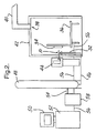
- Figure 2 is a view particularly highlighting a kinetic spray system layout.
- Figure 3 is a side view particularly highlighting the deposition and plastic deformation of copper particles onto a silver bond layer formed upon an alumina substrate.
- Figure 4 is an illustration of deposited copper particles deposited onto and bridging strips of silver bond layers formed upon an alumina substrate.
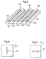
- Figure 5 is a partial sectional and a partial perspective view of an alumina substrate with parallel strips of silver bond layers having layers of copper particles deposited thereon.
- Figure 6 is an end view of a kinetic spray nozzle oriented such that the rectangular exit aperture is in a vertical position.
- Figure 7 is an end view of a kinetic spray nozzle oriented such that the rectangular exit aperture is rotated 90°, as compared to Figure 6, and is in a horizontal position.
- copper-based circuits formed by kinetic spray are set forth hereinbelow.
- copper-based circuits formed according to the present invention are demonstrated to have thicknesses of up to and exceeding several millimeters per pass. Substantially thicker coatings are obtainable from multiple passes. As a result of such thicknesses, copper-based circuits formed according to the present invention inherently have high-current and better heat spreading and thermal management capabilities suitable for high-power electronic applications.
- Figure 1 is a cross-sectional view particularly highlighting a kinetic spray nozzle 10 for directing copper particles 100 onto one or more silver bond layers 62 formed upon a substrate 60.
- the spray nozzle 10 used in the experiments was a de Laval type which has a hollow, conic-shaped chamber which defines a converging sonic region 12 within the nozzle 10.
- the converging sonic region 12 has a decreasing diameter which ultimately forms a small circular aperture which defines a throat 16 within the nozzle 10.
- another hollow chamber defines a supersonic region 14.
- the supersonic region 14 diverges and forms a rectangular exit aperture 20 at the exit end of the nozzle 10.
- the exit aperture of a powder feed line 26 is introduced into nozzle 10 at the non-converging end of the sonic region 12.
- the powder feed line 26 thereby serves as means for introducing into the sonic region 12 one or more pre-selected powders containing copper particles.
- Further incorporated in the non-converging end of the sonic region 12 is a structure having one or more apertures defining a flow straightener 22.
- the flow straightener 22 serves as means for permitting the streamlined introduction of a gas into the non-converging end of the sonic region 12.
- the gas is directed through the flow straightener 22 by a gas conduit 28 leading from an in-line gas heater 32.
- the gas heater 32 can produce a gas temperature as high as 650° C.
- a thermocouple 30 which monitors the temperature of the gas passing through the conduit 28.
- the sonic region 12 defines a mixing chamber 18 in which a powder introduced by the feed line 26 and a gas introduced by the flow straightener 22 are mixed before being expelled via the throat 16 and the supersonic region 14 of the nozzle 10.
- a pressure sensor 24 is used.
- FIG. 2 shows the general layout of a kinetic spray system in accordance with the present invention. Consistent with the present invention, it is to be understood that other spray systems, such as, for example, the spray system disclosed in United States Patent Number 5,302,414, issued to Alkhimov et al on April 12, 1994, and as disclosed in allowed Serial No. 09/343,016 owned by the assignee of the present invention, each of which are incorporated herein by reference in its entirety, is adaptable for utilization consistent with the present invention as well.
- the nozzle 10 and gas heater 32 are situated within a spray deposition chamber 42.
- the chamber 42 has a vent 38 which permits the evacuation of gas and/or particulates via a conduit 40 which is connected to, for example, a dust collector.
- a target mounting pad 34 which is supported on a manipulatable x-y-z rotation motion stage 36. The target mounting pad 34 is selectively moved and positioned relative to the exit aperture 20 of the nozzle 10 by the motion stage 36.
- a high-pressure powder feeder 44 situated outside of the spray deposition chamber 42.
- a preferred powder feeder is sold by Powder Feeder Dynamics, Inc., under the designation Markxuird Precision Powder Feeder.
- the powder feeder 44 delivers one or more powders, comprising copper particles or an alloy thereof, into the mixing chamber 18 of the nozzle 10 via the powder feed line 26.
- an air compressor 58 pneumatically connected to an air ballast tank 48 via an air conduit 54.
- the air compressor 58 is preferably a Bauer-type air compressor which provides pressures of up to about 3.4 MPa (500 psi).
- the compressor 58 delivers pressurized air or gas into tank 48, which serves as a temporary reservoir of pressurized air or gas, for ultimate delivery into heater 32 via a conduit 46.
- a computer 52 with user monitor 50 is electronically connected via a computer control line 56 to the above-described components of the kinetic spray system.
- the computer 52 serves to control and monitor the gas inlet temperature within the nozzle 10 by electronically controlling the temperature of the in-line heater 32 and by electronically sensing the gas temperature with the thermocouple 30.
- the computer 52 monitors and controls the gas inlet pressure within the nozzle 10 by electronically controlling the air compressor 58 in response to the pressure within the mixing chamber 18 determined by the pressure sensor 24.
- the inlet pressure and the powder feed rate associated with the powder feeder 44 are also monitored and controlled by the computer 52.
- the computer 52 also controls the rate and direction of movement of the motion stage 36. In this way, the rate of movement and positioning of the target mounting pad 34 with respect to the exit aperture 20 of the nozzle 10 is closely controlled.
- a target according to the present invention is detachably mounted to the mounting pad 34.
- the target comprises an electrically insulative substrate 60 having, in this embodiment, horizontal bond layers 62 formed on the substrate 60.
- the substrate should have a breakdown voltage of at least 500 volts for automotive applications, and of that order for SCR's, high power MOSFET's and microprocessors in non-automotive applications and comprises, but is not limited to, insulators such as aluminum-oxide (alumina, Al 2 O 3 ), aluminum-nitride (AlN) or boron-nitride (BN).
- insulators such as aluminum-oxide (alumina, Al 2 O 3 ), aluminum-nitride (AlN) or boron-nitride (BN).
- Such substrate materials are preferred because of their beneficial thermal management and heat spreading capabilities as well as their desirable breakdown voltages.
- alumina has a thermal conductivity of about 25 to 35 Watts/(m °K) and a breakdown voltage of about 1x10 7 volts/meter.
- Aluminum-nitride has a thermal conductivity of about 175 to 220 Watts/(m °K) and a breakdown voltage of 1.5x10 7 volts/meter.
- boron-nitride has a thermal conductivity of about 700 Watts/(m °K).
- the bond layers 62 preferably comprise silver or a silver alloy, such as a silver-palladium composition having a three-to-one (3:1) weight ratio, or a silver-platinum composition having 99:1 weight ratio.
- Silver or a silver alloy is utilized because silver has inherent plasticity and, therefore, can soak up the kinetic energies of the copper particles as they impact the bond layers 62 for successful deposition.
- utilizing silver in the bond layers 62 as opposed to utilizing silver-palladium or silver-platinum, is generally preferred since a silver-palladium or silver-platinum composition is generally more expensive than silver alone.
- the bond layers 62 are formed upon the substrate 60 before the substrate 60 is detachably mounted to the mounting pad 34 for spraying.
- Silver-based material is not the only possible bond material. Any plastically deformable material would suffice, such as metals including, but not limited to, Ni, Cu, Zn, Nb, Ta, W, Sn, Sb, and mixtures thereof.
- the bond layers 62 are preferably formed by a conventional screen printing technique and facilitate the deposition of the copper particles upon the substrate 60. Copper particles which would not otherwise adhere very well to the substrate 60 are deposited onto the substrate 60 with a bond layer 62. It is to be understood that the bond layers 62 are printed onto the substrate 60 in predetermined patterns to thereby define the ultimate circuit patterns formed when the copper particles are deposited onto the bond layers 62. Alternatively, the copper particle size distribution can be adjusted so that they will adhere to the substrate 60 without the silver bond layer. Copper particles in the size range of 25 to 45 micrometers have been deposited on and adhered to alumina substrates without a silver bond layer by the method of the invention. The best adhesion was achieved for copper particles less than 25 micrometers.
- copper particle size distribution can be adjusted so that they adhere well to the substrate. It is preferred to have particle size of 25 microns or less. The lower limit to particle size is a practical one since if particles are too small, on the order of 5 microns or less, they tend to drift away due to aerodynamics rather than deposit on the substrate.
- a powder of copper-based particles is delivered into the mixing chamber 18 of the nozzle 10 via feed line 26 from powder feeder 44.
- pressurized and heated gas is also delivered into the mixing chamber 18 via conduit 28 from in-line heater 32.
- the copper particles are entrained within the streamlined flow of a carrier gas established by the flow straightener 22 to thereby form a jet.
- both the carrier gas and the copper particles 100 exit the nozzle 10 at supersonic velocities.
- the nozzle 10 facilitates carrier gas velocities greater than 1000 m/s while copper particle velocities range from about 500 m/s to about 600 m/s.
- copper particle velocities are dependent on particle size such that the smaller copper particles have velocities which generally approach the maximum carrier gas velocity while the larger copper particles have slower velocities.
- the copper particles 100 are expelled from the nozzle 10 via the exit aperture 20 such that, ultimately, the copper particles 101 are deposited onto a bond layer 62 formed on the substrate 60.
- kinetic spray processing according to the present invention is then complete.
- the substrate 60 can then be removed from the mounting pad 34.
- the exit aperture 20 of the nozzle 10 is selectively spaced away from the bond layers 62 on the substrate 60 by a predetermined standoff distance 64.
- the standoff distance 64 can be adjusted by computer-controlled manipulation of the motion stage 36.
- the purpose of heating the gas within the kinetic spray system with the heater 32 is not to heat the copper particles but rather to increase the velocity of the carrier gas through the nozzle 10. More particularly, the carrier gas is heated to increase the shock wave velocity in the gas. As a result, the velocities of the copper particles are also increased as they move with the carrier gas through the nozzle 10. In this way, the rate of copper deposition can generally be controlled by merely controlling the temperature of the carrier gas.
- the velocities of the copper particles are directly related to the square root of the temperature of the carrier gas, and the velocities of the copper particles are inversely related to the square root of the mass of the carrier gas.
- the carrier gas temperature is generally maintained within the range of about 100°C to about 500°C.
- the copper particles are vicariously heated as well, but only to temperatures well below the melting temperatures of the copper particles.
- copper has a melting temperature of about 1083°C (1357°K).
- the maximum temperature of the carrier gas in the kinetic spray system according to the present invention is only about one-half (1 ⁇ 2) of the melting temperature of the copper particles.
- the copper particles impact the silver bond layers 62 in solid form, not molten form.
- helium should be utilized in the kinetic spray system instead of air, for helium has a smaller molecular weight than air, and the shock wave velocities scale inversely with the square root of the molecular weight of the gas.
- Figure 3 is a side view illustrating the deposition and plastic deformation of copper particles onto the bond layer 62 formed upon the substrate 60.
- the copper particles are neither melted nor softened prior to impingement onto the bond layers 62 of the substrate 60.
- the copper particles are roughly spherical and are sieved to have particle diameter sizes of about 15 to 150 microns, but could be 45 to 63 microns, and are accelerated to high linear rates of speed such that the copper particles are plastically deformed and deposited onto the bond layers 62 of the substrate 60.
- the plastic deformation of the copper particles is the result of particulate kinetic energy being converted to mechanical deformation, strain energy and thermal energy upon impact with the substrate 60.
- the bond layer 62 facilitates the transference of the kinetic energy of a copper particle to ensure indirect adhesion to the substrate 60.
- the copper particles are directed substantially normal to the surface of the bond layers 62 on the substrate 60. In another embodiment, no bond layer is required. Rather, the kinetic energy of the copper particles is transferred to thermal and mechanical energies primarily by plastic deformation of the copper particles upon impact directly with the electrically insulating substrate.
- the aspect ratios of the copper particles are substantially changed such that the copper particles become somewhat pancake-like and are deformed into conformation with the substrate 60 and with each other. That is, after the initial copper particles impact and adhere to the bond layer 62 of the substrate 60, the subsequent copper particles then impact the previously-deposited particles, deform, and bond to produce a rapidly increasing copper coating over the bond layer 62 on the substrate 60. As the copper particles accumulate over the bond layers 62, the copper particles also tend to mechanically interlock with each other as well. In addition, the conversion of the particulate kinetic energy to thermal energy upon impact may cause thermal softening of the copper particles which also facilitates their bonding and/or interlocking with each other. As layers of copper particles are deposited over the bond layers 62, the early deposited copper layers formed closest to the bond layers 62 tend to have relatively low overall porosities. As a result, good electrical conductivity through the copper lines formed on the bond layers 62 is achieved.
- the bonding mechanism for the kinetic spray process is a complex process including both particle-bond layer interaction and particle-particle interaction.
- copper particles 104 which first impact the bond layer 62 at high velocities tend to deform and produce craters in the surface of the bond layer 62 and ultimately define a first-layer build up of particles on the bond layer 62.
- the range of kinetic energies of the first copper particles 104 includes energies both sufficient to crater the bond layer 62 and not bond thereto and sufficient to crater the bond layer 62 and successfully bond thereto. These first copper particles 104 are the most prone to extensive plastic deformation.
- Some mechanical bonding also occurs in this first layer of copper particles 104 as the particles deform and fill voids in the cratered surface of the bond layer 62. Those copper particles which bond directly to the bond layer 62 thereby provide a bonding surface for subsequent incoming copper particles.
- a second layer of copper particles 103 is formed over the first layer 104 wherein the particles comprising the second layer are plastically deformed and conformed to fill the particle voids defined by the first layer of particles 104.
- void reduction between particles occurs to the point where mechanical interlocking and particle-to-particle bonding is achieved.
- Last incoming copper particles 102 impact and peen the second layer of particles 103 thereby generally contributing to the void reduction and mechanical interlocking between particles in the second layer. These last particles 102 are not plastically deformed to the extent of the first and second layers of particles and generally experience minimal particle deformation.
- these last particles 102 tend to rotate and realign themselves upon impact so that they follow paths of least resistance and fill voids established by the second layer of particles 103. Due to the minimal deformation of the last particles 102, the copper layer defined by these last particles 102 has more voids and is, therefore, more porous than both the first layer of particles 104 and the second layer of particles 103. More particularly, the copper layer defined by these last particles 102 is characterized by having minimal mechanical interlocking, minimal heat generation, and minimal particle-to-particle bonding.
- FIG. 5 is a partial sectional and a partial perspective view of the substrate 60, after copper deposition, with parallel strips of bond layers 62 having layers of deposited copper particles 106 thereon.
- the basic copper-based circuit configuration in Figure 5 includes an electrically insulative substrate 60, a bond layer 62 which is formed over select portions of the substrate 60 according to a desired shape of the circuit, and an electrically conductive layer 106 including plastically deformed particles of copper deposited on the bond layer 62.
- the substrate 60 may comprise electrical insulators including, but not limited to, aluminum oxide, aluminum nitride, or boron nitride.
- the bond layer 62 preferably includes silver or a silver alloy, such as, for example, silver-palladium.
- Silver-based material is not the only possible bond material. Any plastically deformable material would suffice, such as metals including, but not limited to, Ni, Cu, Zn, Nb, Ta, W, Sn, Sb, and mixtures thereof.
- the bond layer 62 has a preferred thickness of approximately 10 to 12 micrometers.
- a very significant advantage of the present invention is that a copper-based circuit formed by kinetic spray according to the present invention generally does not require the copper particles to be sprayed through a precisely positioned, pre-patterned mask to form predetermined circuit patterns on the substrate 60. More particularly, relatively larger copper particles do not adhere directly to the substrate 60. Since such particles only adhere to the bond layers 62, the kinetic spray system according to the present invention need only be generally directed to the substrate 60 without a mask. This arrangement is readily adaptable for commercial use since the copper particles 100 expelled via the exit aperture 20 of the spray nozzle 10 will generally only adhere to the pre-patterned bond layers 62.
- Formation of a copper-based circuit by kinetic spray according to the present invention is further demonstrated by way of the following examples.
- the kinetic spray system equipment utilized in this example is generally illustrated in Figure 1 and in Figure 2.
- a carrier gas was delivered to the mixing chamber 18 via the flow straightener 22 at a pressure of about 2 MPa (300 psi) and at a temperature that was controlled between 100°C and 500°C.
- a copper powder was delivered to the mixing chamber 18 at a pressure of about 2.4 MPa (350 psi).
- the mixing chamber 18 of the nozzle 10 emptied into the throat 16, and the throat 16 had a selected diameter such that the carrier gas and copper particles achieved a supersonic velocity as they exited the nozzle 10.
- the copper particles accelerated to high velocities due to drag effects with the carrier gas. Such high velocities caused the copper particles to plastically deform as they impacted the bond layers 62 of the substrate 60, thereby forming a multi-layered copper-based circuit on the substrate 60.
- aluminum oxide (alumina) substrates measuring 140 by 80 millimeters and having a thickness of about one millimeter, were used.
- the alumina substrates had screen-printed silver (Ag) bond layer coatings having thicknesses of approximately 12 micrometers.
- both solid and patterned bond layer coatings were used.
- the copper powder was sieved such that the copper particles generally had diameters within the range of approximately 45 micrometers to 63 micrometers.
- the powder delivery was controlled by the auger speed of rotation of the powder feeder.
- the standard revolutions-per-minute (rpms) used by the powder feeder in this example was 500. Increasing or decreasing the delivery rate resulted in a corresponding increase or decrease in the copper film thickness.
- powder feeder pressure 2.4 MPa (350 psi)
- carrier gas (air) pressure 2.0 MPa (300 psi)
- nozzle-to-target standoff distance 19 millimeters (0.75 inch)
- powder feeder delivery rate 500 rpm.
- the variable parameters in this example included the carrier gas temperature (100 to 500°C), traverse speed of the target, and the size of nozzle utilized.
- Nozzles of different sizes were used in this example.
- the standard nozzle was a short nozzle with length of entire nozzle 110mm, dimensions of exit aperture 10mm x 2mm.
- the other nozzle was longer than the short nozzle and thereby permitted longer residence time for the copper particles to accelerate to higher velocities.
- the longer nozzle dimension was length of entire nozzle 300mm, dimensions of exit aperture 28mm x 2mm.
- the carrier gas temperature is thought to be material dependent and here was about 150°C to 635°C (300°F to 1200°F).
- the traverse target speed is thought to be dependent on a desired coating thickness and here was 13 mm/s.
- the number of spray passes over a target is optional. Here, only one pass was used. Any number of passes can be used based on desired copper thickness.
- the nozzle type was short.
- the carrier gas temperature was varied between 150°C and 450°C.
- the resultant thickness of the copper particle coating was 0.65 millimeters but showed signs of surface oxidation.
- Samples prepared as per this example had a copper coating thickness of 0.5 mm at 350°C, and a thickness of 0.18 mm at a temperature of 150°C. Within this temperature range, no signs of surface oxidation were present. At temperatures below 150°C, however, results indicated that a continuous copper coating was difficult to obtain.
- the traverse speed was changed from 6.5 mm/s to 13, 65, and 130 mm/s.
- the corresponding copper film thicknesses produced were 0.31 mm, 0.55 mm, 0.07 mm, and 0.02 mm.
- the general trend for the copper film thickness to drop with increases in the traverse target speed is due to the reduced dwell time of the nozzle in front of the target.
- the logic of this trend was generally not applicable to the slower traverse speed of 6.5 mm/s, whereunder the copper film thickness actually decreased rather than increased. Such is thought to be due to the competition between the deposition forces attempting to deposit the copper particles and the less energetic particles that sand blast the silver-coated surface of the substrate.
- the thickest copper film attainable from a single pass deposition was 1.2 millimeters at a traverse target speed of 13 mm/s and at a carrier gas temperature of 500°C.
- the width of the horizontally sprayed copper strip was over 10 millimeters.
- the resultant thickness of the copper film was about 0.5 mm, depending on the carrier gas temperature, and no signs of delamination of the copper film were present.
- the width of the copper spray pattern on a horizontally moving target was reduced to about 3 millimeters while the copper film thickness was about 0.3 millimeter.
- the adhesion of the copper particles to the silver coating on the substrate was successfully maintained.
- the copper spray had to be directed through a pre-pattemed mask during deposition.
- the traverse speed of the horizontally moving target in front of the spray nozzle was increased to about 100 mm/s, the adhesion of the copper particles onto the silver coating was improved.
- the thickness of the copper coating was only about 0.1 millimeter.
- the first batch was sprayed with one pass, and the carrier gas (air) temperature was set at about 400°C (800°F).
- the traverse target speed was set at about 19 mm/s (0.75 inch/s). At such settings, copper films having a thickness of about 0.37 mm (15 mils) were successfully produced.
- the second batch was sprayed with two passes, and the carrier gas (air) temperature was slightly reduced to 370°C (725°F) in order to avoid surface oxidation. At such settings, copper films having thicknesses which exceeded 0.5 mm (20 mils) were successfully produced.
- This example demonstrated the operability of the method for directly spraying copper particles onto ceramics without the use of a bond layer.
- copper coating was applied having good adhesion to the ceramic substrate for selected particle size.
- four different size groups of copper powder particles were prepared, the ranges were 63 to 90 micrometers, 45 to 63 micrometers, 25 to 45 micrometers, and less than 25 micrometers. Each of these groups of particles was obtained by sieving. For the smallest group, no single particle had a size greater than 25 micrometers.
- the ceramic substrates were alumina (Al 2 O 3 ) and aluminum nitride (AlN). Both the short and long nozzles were used.
- powder feeder pressure 2.4 MPa (350 psi)
- carrier gas (air) pressure 2.0 MPa (300 psi)
- standoff distance between nozzle and substrate 19 mm (0.75 inch)
- powder delivery rate 500 rpm
- carrier gas temperature 370°C (700°F).
- the experimental set-up was the same as shown in Figure 1, except that the bond layer 62 was not present. Therefore, the copper particles 100 were sprayed directly onto substrate 60 and deposited as an adhered layer on substrate 60.
- the powder size range of 25 to 45 micrometers was sprayed directly on alumina (Al 2 O 3 ) and a continuous uniform coating was produced using the short nozzle.
- the long nozzle for the same powder size, did not produce a continuous coating on alumina.
- the same Cu powder size 25 to 45 micrometers was sprayed on aluminum nitride substrates (AlN) using both nozzles (short and long). It was possible to produce a continuous copper coating.
Landscapes
- Engineering & Computer Science (AREA)
- Chemical & Material Sciences (AREA)
- Manufacturing & Machinery (AREA)
- Microelectronics & Electronic Packaging (AREA)
- Chemical Kinetics & Catalysis (AREA)
- Materials Engineering (AREA)
- Mechanical Engineering (AREA)
- Metallurgy (AREA)
- Organic Chemistry (AREA)
- Manufacturing Of Printed Wiring (AREA)
- Parts Printed On Printed Circuit Boards (AREA)
- Other Surface Treatments For Metallic Materials (AREA)
Abstract
Description
- The present invention relates to copper-based interconnect circuits formed on substrates.
- With the increased incorporation of electronic components and electrical systems in modern motor vehicles, there is a greater need for components and systems having circuits with high-current and better thermal management capabilities. Circuits with such capabilities are necessary to satisfy the high-power applications and requirements which are common in such modem motor vehicles. In addition to automotive applications, such circuits may lead to improved thermal management in electronic devices ranging from SCR's to high power MOSFET's and microprocessors. In general, for a circuit to meet such criteria, the metal conducting path must be sufficiently thick to minimize heat generation and to conduct or spread the heat or thermal energy to assist in circuit cooling.
- One prior art solution to fabricating thick circuits with high-current and better thermal management capabilities has been to utilize ultra-thick film technology in which a circuit line of silver is screen printed in single or multiple layers, depending on the required thickness of the circuit. For examples, see United States Patent Number 5,395,679 issued to Myers et al on March 7, 1995, and see also United States Patent Number 5,527,627 issued to Lautzenhiser et al on June 18, 1996. However, in attempting to form a circuit line of a particular thickness by overlay printing of multiple layers of silver, the first layer is limited to a practical thickness of only about 0.15 is millimeters (6 mils). Additional layers are limited to thicknesses of only about 0.075 millimeters (3 mils). In addition to having to print multiple layers on top of each other to obtain a circuit line with sufficient thickness, it is also necessary to fire each deposited layer before proceeding to deposit the next layer. Thus, a first drawback to this method is that it requires multiple processing steps and additional time to form a sufficiently thick multi-layer circuit line wherein each layer must be fired before the next layer can be applied. In addition, a second drawback to this method is that, when dealing with surface mount technologies (SMT), there are significant problems associated with soldering a pre-fabricated electronic component to a silver circuit line. This includes silver leaching during the solder reflow process, and the undesired growth of brittle tin-silver intermetallic compounds.
- Another approach is to utilize a process for the metallization of alumina called "direct bond copper." See, for example, United States Patent Number 3,993,411 issued to Babcock et al on November 23, 1976. In this process, a thin copper foil is directly bonded to an alumina substrate under a very stringently controlled environment. The desired circuit line, which is to be formed from the copper foil, is covered and protected with a chemical-resist mask, and the remaining copper foil which is not protected by the mask is thereafter etched away. In this way, the remaining un-etched copper foil defines the circuit line. However, with this approach, the thickness of the copper circuit line is limited to about 0.5 millimeters (20 mils) because a thicker copper circuit line would begin to exhibit poorer adhesion to the alumina substrate. In addition, a thicker copper foil is more expensive to process because of the additional time required to etch the unprotected thicker copper foil.
- Although both of the above-mentioned methods involve standard processes, neither one of them provides a low-cost way to fabricate sufficiently thick circuit lines having high-current and good thermal management capabilities. Thus, there remains a present need in the art for the low-cost fabrication of thick films of copper, preferably several millimeters thick, having high-current and good thermal management capabilities. An example of a high current application is one requiring electrical current on the order of 10 to 200 amperes.
- The present invention provides a copper-based circuit for use in high-current applications. According to one embodiment of the invention, the copper-based circuit has an electrically insulative substrate, a bond layer including silver which is formed over select portions of the substrate according to a desired shape of the circuit, and an electrically conductive layer including plastically deformed particles of copper deposited on the bond layer. In another embodiment of the invention, the copper particles are directly deposited onto a substrate without utilizing a bond layer. The copper particles are selected to have particle size in a range which permits adherence to the substrate without the bond layer. As used herein, the term particle size refers to the size of particles obtained by sieve. The term particle size and the term particle diameter are typically used interchangeably in the art. Here, as stated, such relates to the dimension obtained by sieving.
- According to preferred embodiments of the present invention, the substrate may include aluminum oxide, aluminum nitride, or boron nitride. The bond layer may include, for example, a silver-palladium alloy. In one embodiment of the present invention, the bond layer has a preferred thickness of approximately 10 to 12 micrometers.
- In another aspect, the present invention also provides a process for forming the copper-based circuit on a substrate. In one aspect, the process includes the steps of providing an electrically insulative substrate, forming a bond layer including silver over select portions of the substrate according to a desired shape of the circuit, and depositing copper on the bond layer. According to one alternative of the process, the silver-based bond layer is placed over select portions of the substrate by a screen printing technique.
- The step of depositing copper on the bond layer includes the steps of introducing copper particles into a pressurized carrier gas, forming the pressurized carrier gas and the copper particles into a supersonic jet, and directing the jet toward the bond layer. The jet has a velocity sufficient to cause plastic deformation of the copper particles onto the bond layer. In this way, an electrically conductive layer is thereby formed on the bond layer and is well-adhered thereto.
- Desirably, each copper particle has a diameter of about 25 micrometers to about 150 micrometers. Preferably, each copper particle has a diameter of about 45 micrometers to about 65 micrometers when deposited onto a bond layer. Preferably, the particles have a size of 45 micrometers or less when deposited without a bond layer. Most preferably, the particles have a size of 25 micrometers or less when deposited onto a substrate without the bond layer. While the powder particles are roughly spherical, the deposited particles have been somewhat flattened (aspect ratios in the range of 3:1 to 5:1). Deposited particles tend to fill available volume (voids) in the coating.
- Preferably, the carrier gas has a pressure of about 1.2 MPa to about 2 MPa, and has a temperature of about 100°C to about 500°C. The jet is preferably directed substantially normal with respect to the surface of the bond layer formed over the substrate. In addition, the jet is directed at the surface of the bond layer on the substrate from a preferred standoff distance of about 4 millimeters to about 45 millimeters, and more preferably from a standoff distance of about 6 millimeters to about 44 millimeters. Most preferably, the jet is directed to the surface of the bond layer from a standoff distance of about 19 millimeters. In this way, the kinetic energies of the copper particles are transferred to the bond layer upon impact such that the copper particles are plastically deformed and will properly accumulate and adhere to the bond layer.
- Advantages, design considerations, and applications of the present invention will become apparent to those skilled in the art when the detailed description of the best mode contemplated for practicing the invention, as set forth hereinbelow, is read in conjunction with the accompanying drawings.
- The present invention will now be described, by way of example, with reference to the following drawings.
- Figure 1 is a cross-sectional view particularly highlighting a spray nozzle for directing copper particles onto a silver bond layer formed upon an alumina substrate.
- Figure 2 is a view particularly highlighting a kinetic spray system layout.
- Figure 3 is a side view particularly highlighting the deposition and plastic deformation of copper particles onto a silver bond layer formed upon an alumina substrate.
- Figure 4 is an illustration of deposited copper particles deposited onto and bridging strips of silver bond layers formed upon an alumina substrate.
- Figure 5 is a partial sectional and a partial perspective view of an alumina substrate with parallel strips of silver bond layers having layers of copper particles deposited thereon.
- Figure 6 is an end view of a kinetic spray nozzle oriented such that the rectangular exit aperture is in a vertical position.
- Figure 7 is an end view of a kinetic spray nozzle oriented such that the rectangular exit aperture is rotated 90°, as compared to Figure 6, and is in a horizontal position.
- The preferred structure and fabrication method for a copper-based circuit formed by kinetic spray, according to the present invention, is set forth hereinbelow. Through experimentation, copper-based circuits formed according to the present invention are demonstrated to have thicknesses of up to and exceeding several millimeters per pass. Substantially thicker coatings are obtainable from multiple passes. As a result of such thicknesses, copper-based circuits formed according to the present invention inherently have high-current and better heat spreading and thermal management capabilities suitable for high-power electronic applications.
- According to a preferred embodiment of the present invention, Figure 1 is a cross-sectional view particularly highlighting a
kinetic spray nozzle 10 for directingcopper particles 100 onto one or more silver bond layers 62 formed upon asubstrate 60. Thespray nozzle 10 used in the experiments was a de Laval type which has a hollow, conic-shaped chamber which defines a convergingsonic region 12 within thenozzle 10. The convergingsonic region 12 has a decreasing diameter which ultimately forms a small circular aperture which defines athroat 16 within thenozzle 10. Opposite the convergingsonic region 12, another hollow chamber defines asupersonic region 14. Thesupersonic region 14 diverges and forms arectangular exit aperture 20 at the exit end of thenozzle 10. - In Figure 1, the exit aperture of a
powder feed line 26 is introduced intonozzle 10 at the non-converging end of thesonic region 12. Thepowder feed line 26 thereby serves as means for introducing into thesonic region 12 one or more pre-selected powders containing copper particles. Further incorporated in the non-converging end of thesonic region 12 is a structure having one or more apertures defining aflow straightener 22. Theflow straightener 22 serves as means for permitting the streamlined introduction of a gas into the non-converging end of thesonic region 12. The gas is directed through theflow straightener 22 by agas conduit 28 leading from an in-line gas heater 32. According to a preferred embodiment of the present invention, thegas heater 32 can produce a gas temperature as high as 650° C. Incorporated within thegas conduit 28 is athermocouple 30 which monitors the temperature of the gas passing through theconduit 28. In this arrangement, thesonic region 12 defines a mixing chamber 18 in which a powder introduced by thefeed line 26 and a gas introduced by theflow straightener 22 are mixed before being expelled via thethroat 16 and thesupersonic region 14 of thenozzle 10. In order to determine the pressure within the mixing chamber 18, apressure sensor 24 is used. - Figure 2 shows the general layout of a kinetic spray system in accordance with the present invention. Consistent with the present invention, it is to be understood that other spray systems, such as, for example, the spray system disclosed in United States Patent Number 5,302,414, issued to Alkhimov et al on April 12, 1994, and as disclosed in allowed Serial No. 09/343,016 owned by the assignee of the present invention, each of which are incorporated herein by reference in its entirety, is adaptable for utilization consistent with the present invention as well. However, as particularly illustrated in Figure 2, the
nozzle 10 andgas heater 32 are situated within aspray deposition chamber 42. Thechamber 42 has a vent 38 which permits the evacuation of gas and/or particulates via aconduit 40 which is connected to, for example, a dust collector. Also within thechamber 42 is atarget mounting pad 34 which is supported on a manipulatable x-y-zrotation motion stage 36. Thetarget mounting pad 34 is selectively moved and positioned relative to theexit aperture 20 of thenozzle 10 by themotion stage 36. - Further in Figure 2, situated outside of the
spray deposition chamber 42 is a high-pressure powder feeder 44. A preferred powder feeder is sold by Powder Feeder Dynamics, Inc., under the designation Markxuird Precision Powder Feeder. Thepowder feeder 44 delivers one or more powders, comprising copper particles or an alloy thereof, into the mixing chamber 18 of thenozzle 10 via thepowder feed line 26. Also situated outside of thechamber 42 is anair compressor 58 pneumatically connected to anair ballast tank 48 via anair conduit 54. In this preferred experimental arrangement, theair compressor 58 is preferably a Bauer-type air compressor which provides pressures of up to about 3.4 MPa (500 psi). Thecompressor 58 delivers pressurized air or gas intotank 48, which serves as a temporary reservoir of pressurized air or gas, for ultimate delivery intoheater 32 via aconduit 46. - Further included in the general layout of the kinetic spray system of Figure 2 is a
computer 52 withuser monitor 50. Thecomputer 52 is electronically connected via acomputer control line 56 to the above-described components of the kinetic spray system. In particular, thecomputer 52 serves to control and monitor the gas inlet temperature within thenozzle 10 by electronically controlling the temperature of the in-line heater 32 and by electronically sensing the gas temperature with thethermocouple 30. In addition, thecomputer 52 monitors and controls the gas inlet pressure within thenozzle 10 by electronically controlling theair compressor 58 in response to the pressure within the mixing chamber 18 determined by thepressure sensor 24. The inlet pressure and the powder feed rate associated with thepowder feeder 44 are also monitored and controlled by thecomputer 52. Finally, thecomputer 52 also controls the rate and direction of movement of themotion stage 36. In this way, the rate of movement and positioning of thetarget mounting pad 34 with respect to theexit aperture 20 of thenozzle 10 is closely controlled. - Referring back to Figure 1, a target according to the present invention is detachably mounted to the mounting
pad 34. In particular, the target comprises anelectrically insulative substrate 60 having, in this embodiment, horizontal bond layers 62 formed on thesubstrate 60. According to a preferred embodiment of the present invention, the substrate should have a breakdown voltage of at least 500 volts for automotive applications, and of that order for SCR's, high power MOSFET's and microprocessors in non-automotive applications and comprises, but is not limited to, insulators such as aluminum-oxide (alumina, Al2O3), aluminum-nitride (AlN) or boron-nitride (BN). Such substrate materials are preferred because of their beneficial thermal management and heat spreading capabilities as well as their desirable breakdown voltages. In particular, alumina has a thermal conductivity of about 25 to 35 Watts/(m °K) and a breakdown voltage of about 1x10⁷ volts/meter. Aluminum-nitride, on the other hand, has a thermal conductivity of about 175 to 220 Watts/(m °K) and a breakdown voltage of 1.5x10⁷ volts/meter. Lastly, boron-nitride has a thermal conductivity of about 700 Watts/(m °K). The bond layers 62, in turn, preferably comprise silver or a silver alloy, such as a silver-palladium composition having a three-to-one (3:1) weight ratio, or a silver-platinum composition having 99:1 weight ratio. Silver or a silver alloy is utilized because silver has inherent plasticity and, therefore, can soak up the kinetic energies of the copper particles as they impact the bond layers 62 for successful deposition. However, utilizing silver in the bond layers 62, as opposed to utilizing silver-palladium or silver-platinum, is generally preferred since a silver-palladium or silver-platinum composition is generally more expensive than silver alone. Moreover, it is possible to spray relatively thick copper layers on the silver, and the palladium is not required. This is because the thick copper inhibits the tin and silver diffusion thereby eliminating the growth of brittle tin-silver compounds at the welded joint. The bond layers 62 are formed upon thesubstrate 60 before thesubstrate 60 is detachably mounted to the mountingpad 34 for spraying. Silver-based material is not the only possible bond material. Any plastically deformable material would suffice, such as metals including, but not limited to, Ni, Cu, Zn, Nb, Ta, W, Sn, Sb, and mixtures thereof. - The bond layers 62 are preferably formed by a conventional screen printing technique and facilitate the deposition of the copper particles upon the
substrate 60. Copper particles which would not otherwise adhere very well to thesubstrate 60 are deposited onto thesubstrate 60 with abond layer 62. It is to be understood that the bond layers 62 are printed onto thesubstrate 60 in predetermined patterns to thereby define the ultimate circuit patterns formed when the copper particles are deposited onto the bond layers 62. Alternatively, the copper particle size distribution can be adjusted so that they will adhere to thesubstrate 60 without the silver bond layer. Copper particles in the size range of 25 to 45 micrometers have been deposited on and adhered to alumina substrates without a silver bond layer by the method of the invention. The best adhesion was achieved for copper particles less than 25 micrometers. Therefore, copper particle size distribution can be adjusted so that they adhere well to the substrate. It is preferred to have particle size of 25 microns or less. The lower limit to particle size is a practical one since if particles are too small, on the order of 5 microns or less, they tend to drift away due to aerodynamics rather than deposit on the substrate. - As illustrated in Figure 1 according to the present invention, a powder of copper-based particles is delivered into the mixing chamber 18 of the
nozzle 10 viafeed line 26 frompowder feeder 44. At the same time, pressurized and heated gas is also delivered into the mixing chamber 18 viaconduit 28 from in-line heater 32. As a result, the copper particles are entrained within the streamlined flow of a carrier gas established by theflow straightener 22 to thereby form a jet. As the carrier gas and the copper particles move through thethroat 16 of thenozzle 10, both the carrier gas and thecopper particles 100 exit thenozzle 10 at supersonic velocities. More particularly, thenozzle 10 facilitates carrier gas velocities greater than 1000 m/s while copper particle velocities range from about 500 m/s to about 600 m/s. In general, copper particle velocities are dependent on particle size such that the smaller copper particles have velocities which generally approach the maximum carrier gas velocity while the larger copper particles have slower velocities. In this way, thecopper particles 100 are expelled from thenozzle 10 via theexit aperture 20 such that, ultimately, thecopper particles 101 are deposited onto abond layer 62 formed on thesubstrate 60. Once deposition of the copper particles is complete and the copper circuit is thereby formed over the bond layers 62 on thesubstrate 60, kinetic spray processing according to the present invention is then complete. Thus, thesubstrate 60 can then be removed from the mountingpad 34. - In the above-described kinetic spray system, it should be noted that the
exit aperture 20 of thenozzle 10 is selectively spaced away from the bond layers 62 on thesubstrate 60 by apredetermined standoff distance 64. Thestandoff distance 64 can be adjusted by computer-controlled manipulation of themotion stage 36. In addition, it is also important to note that the purpose of heating the gas within the kinetic spray system with theheater 32 is not to heat the copper particles but rather to increase the velocity of the carrier gas through thenozzle 10. More particularly, the carrier gas is heated to increase the shock wave velocity in the gas. As a result, the velocities of the copper particles are also increased as they move with the carrier gas through thenozzle 10. In this way, the rate of copper deposition can generally be controlled by merely controlling the temperature of the carrier gas. That is, in general formulaic terms, the velocities of the copper particles are directly related to the square root of the temperature of the carrier gas, and the velocities of the copper particles are inversely related to the square root of the mass of the carrier gas. In the kinetic spray system according to the present invention, the carrier gas temperature is generally maintained within the range of about 100°C to about 500°C. Of course, in the process, the copper particles are vicariously heated as well, but only to temperatures well below the melting temperatures of the copper particles. In particular, copper has a melting temperature of about 1083°C (1357°K). Thus, the maximum temperature of the carrier gas in the kinetic spray system according to the present invention is only about one-half (½) of the melting temperature of the copper particles. As a result, the copper particles impact the silver bond layers 62 in solid form, not molten form. Furthermore, if a particularly high carrier gas velocity is desired, helium should be utilized in the kinetic spray system instead of air, for helium has a smaller molecular weight than air, and the shock wave velocities scale inversely with the square root of the molecular weight of the gas. - Figure 3 is a side view illustrating the deposition and plastic deformation of copper particles onto the
bond layer 62 formed upon thesubstrate 60. According to the present invention, the copper particles are neither melted nor softened prior to impingement onto the bond layers 62 of thesubstrate 60. According to the present invention, the copper particles are roughly spherical and are sieved to have particle diameter sizes of about 15 to 150 microns, but could be 45 to 63 microns, and are accelerated to high linear rates of speed such that the copper particles are plastically deformed and deposited onto the bond layers 62 of thesubstrate 60. The plastic deformation of the copper particles is the result of particulate kinetic energy being converted to mechanical deformation, strain energy and thermal energy upon impact with thesubstrate 60. That is, in order for a given copper particle to adhere, the collision with thebond layer 62 cannot be purely elastic. Instead, the collision must be substantially inelastic, and the copper particle must lose enough of its kinetic energy such that it cannot escape from thebond layer 62 formed on thesubstrate 60. According to the present invention, thebond layer 62 facilitates the transference of the kinetic energy of a copper particle to ensure indirect adhesion to thesubstrate 60. To even further help ensure this transference of kinetic energy, the copper particles, according to the present invention, are directed substantially normal to the surface of the bond layers 62 on thesubstrate 60. In another embodiment, no bond layer is required. Rather, the kinetic energy of the copper particles is transferred to thermal and mechanical energies primarily by plastic deformation of the copper particles upon impact directly with the electrically insulating substrate. - As a result of the impact with the bond layers 62 on the
substrate 60, the aspect ratios of the copper particles are substantially changed such that the copper particles become somewhat pancake-like and are deformed into conformation with thesubstrate 60 and with each other. That is, after the initial copper particles impact and adhere to thebond layer 62 of thesubstrate 60, the subsequent copper particles then impact the previously-deposited particles, deform, and bond to produce a rapidly increasing copper coating over thebond layer 62 on thesubstrate 60. As the copper particles accumulate over the bond layers 62, the copper particles also tend to mechanically interlock with each other as well. In addition, the conversion of the particulate kinetic energy to thermal energy upon impact may cause thermal softening of the copper particles which also facilitates their bonding and/or interlocking with each other. As layers of copper particles are deposited over the bond layers 62, the early deposited copper layers formed closest to the bond layers 62 tend to have relatively low overall porosities. As a result, good electrical conductivity through the copper lines formed on the bond layers 62 is achieved. - As Figure 3 illustrates, the bonding mechanism for the kinetic spray process according to the present invention is a complex process including both particle-bond layer interaction and particle-particle interaction. In particular,
copper particles 104 which first impact thebond layer 62 at high velocities tend to deform and produce craters in the surface of thebond layer 62 and ultimately define a first-layer build up of particles on thebond layer 62. The range of kinetic energies of thefirst copper particles 104 includes energies both sufficient to crater thebond layer 62 and not bond thereto and sufficient to crater thebond layer 62 and successfully bond thereto. Thesefirst copper particles 104 are the most prone to extensive plastic deformation. Some mechanical bonding also occurs in this first layer ofcopper particles 104 as the particles deform and fill voids in the cratered surface of thebond layer 62. Those copper particles which bond directly to thebond layer 62 thereby provide a bonding surface for subsequent incoming copper particles. - Further in Figure 3, after the first layer of
copper particles 104 is established, a second layer ofcopper particles 103 is formed over thefirst layer 104 wherein the particles comprising the second layer are plastically deformed and conformed to fill the particle voids defined by the first layer ofparticles 104. In this second layer ofcopper particles 103, void reduction between particles occurs to the point where mechanical interlocking and particle-to-particle bonding is achieved. Lastincoming copper particles 102 impact and peen the second layer ofparticles 103 thereby generally contributing to the void reduction and mechanical interlocking between particles in the second layer. Theselast particles 102 are not plastically deformed to the extent of the first and second layers of particles and generally experience minimal particle deformation. However, theselast particles 102 tend to rotate and realign themselves upon impact so that they follow paths of least resistance and fill voids established by the second layer ofparticles 103. Due to the minimal deformation of thelast particles 102, the copper layer defined by theselast particles 102 has more voids and is, therefore, more porous than both the first layer ofparticles 104 and the second layer ofparticles 103. More particularly, the copper layer defined by theselast particles 102 is characterized by having minimal mechanical interlocking, minimal heat generation, and minimal particle-to-particle bonding. - Once deposition of copper particles according to the present invention is finished, the
substrate 60 can then be removed from the mountingpad 34 of the kinetic spray system. Figure 5 is a partial sectional and a partial perspective view of thesubstrate 60, after copper deposition, with parallel strips ofbond layers 62 having layers of depositedcopper particles 106 thereon. The basic copper-based circuit configuration in Figure 5 includes anelectrically insulative substrate 60, abond layer 62 which is formed over select portions of thesubstrate 60 according to a desired shape of the circuit, and an electricallyconductive layer 106 including plastically deformed particles of copper deposited on thebond layer 62. Thesubstrate 60 may comprise electrical insulators including, but not limited to, aluminum oxide, aluminum nitride, or boron nitride. Thebond layer 62 preferably includes silver or a silver alloy, such as, for example, silver-palladium. Silver-based material is not the only possible bond material. Any plastically deformable material would suffice, such as metals including, but not limited to, Ni, Cu, Zn, Nb, Ta, W, Sn, Sb, and mixtures thereof. Thebond layer 62 has a preferred thickness of approximately 10 to 12 micrometers. - A very significant advantage of the present invention is that a copper-based circuit formed by kinetic spray according to the present invention generally does not require the copper particles to be sprayed through a precisely positioned, pre-patterned mask to form predetermined circuit patterns on the
substrate 60. More particularly, relatively larger copper particles do not adhere directly to thesubstrate 60. Since such particles only adhere to the bond layers 62, the kinetic spray system according to the present invention need only be generally directed to thesubstrate 60 without a mask. This arrangement is readily adaptable for commercial use since thecopper particles 100 expelled via theexit aperture 20 of thespray nozzle 10 will generally only adhere to the pre-patterned bond layers 62. Thus, inadvertently misdirecting copper particles onto areas of thesubstrate 60 not covered by the bond layers 62 is generally of no consequence, for the relatively larger copper particles generally will not adhere directly to thesubstrate 60 itself. However, in utilizing a kinetic spray process according to the present invention, the strips ofbond layers 62 must generally be sufficiently spaced apart upon thesubstrate 60 to avoid undesired bridging of deposited copper between adjacent strips of bond layers 62. Figure 4 is an illustration of the bridging phenomenon wherein depositedcopper particles 105 bridge parallel strips ofbond layers 62 formed upon thesubstrate 60. As stated, by proper selection of process parameters such bridging is avoided. - Formation of a copper-based circuit by kinetic spray according to the present invention is further demonstrated by way of the following examples.
- The kinetic spray system equipment utilized in this example is generally illustrated in Figure 1 and in Figure 2. A carrier gas was delivered to the mixing chamber 18 via the
flow straightener 22 at a pressure of about 2 MPa (300 psi) and at a temperature that was controlled between 100°C and 500°C. Simultaneously, a copper powder was delivered to the mixing chamber 18 at a pressure of about 2.4 MPa (350 psi). The mixing chamber 18 of thenozzle 10 emptied into thethroat 16, and thethroat 16 had a selected diameter such that the carrier gas and copper particles achieved a supersonic velocity as they exited thenozzle 10. The copper particles accelerated to high velocities due to drag effects with the carrier gas. Such high velocities caused the copper particles to plastically deform as they impacted the bond layers 62 of thesubstrate 60, thereby forming a multi-layered copper-based circuit on thesubstrate 60. - In this example, aluminum oxide (alumina) substrates, measuring 140 by 80 millimeters and having a thickness of about one millimeter, were used. The alumina substrates had screen-printed silver (Ag) bond layer coatings having thicknesses of approximately 12 micrometers. Here, both solid and patterned bond layer coatings were used. In addition, the copper powder was sieved such that the copper particles generally had diameters within the range of approximately 45 micrometers to 63 micrometers. The powder delivery was controlled by the auger speed of rotation of the powder feeder. The standard revolutions-per-minute (rpms) used by the powder feeder in this example was 500. Increasing or decreasing the delivery rate resulted in a corresponding increase or decrease in the copper film thickness.
- In this example, the following spraying conditions were generally held constant: powder feeder pressure = 2.4 MPa (350 psi), carrier gas (air) pressure = 2.0 MPa (300 psi), nozzle-to-target standoff distance = 19 millimeters (0.75 inch), and powder feeder delivery rate = 500 rpm. The variable parameters in this example included the carrier gas temperature (100 to 500°C), traverse speed of the target, and the size of nozzle utilized.
- Nozzles of different sizes were used in this example. The standard nozzle was a short nozzle with length of entire nozzle 110mm, dimensions of exit aperture 10mm x 2mm. The other nozzle, was longer than the short nozzle and thereby permitted longer residence time for the copper particles to accelerate to higher velocities. The longer nozzle dimension was length of entire nozzle 300mm, dimensions of exit aperture 28mm x 2mm.
- With the above kinetic spray conditions in place, results demonstrated that spraying copper particles over silver-coated alumina produce good adhesion, and a continuous layer of copper particles was formed by the kinetic spray. More particularly, for copper particles having diameters of about 45 to 63 micrometers, the operating window for various parameters which produced a well-adhered layer of copper particles over a silver-coated alumina substrate was determined. The most preferred values for these operating parameters are: powder feeder pressure = 2.4 MPa (350 psi), carrier gas (air) pressure = 2.0 MPa (300 psi), standoff distance between nozzle and substrate = 19 mm (0.75 inch), and powder delivery rate = 500 rpm. The carrier gas temperature is thought to be material dependent and here was about 150°C to 635°C (300°F to 1200°F). The traverse target speed is thought to be dependent on a desired coating thickness and here was 13 mm/s. The number of spray passes over a target is optional. Here, only one pass was used. Any number of passes can be used based on desired copper thickness. Here, the nozzle type was short.
- Utilizing the above operating conditions in this example, the carrier gas temperature was varied between 150°C and 450°C. At the highest temperature, the resultant thickness of the copper particle coating was 0.65 millimeters but showed signs of surface oxidation. Previous experimentation indicated that this oxidation occurred only at the surface and did not penetrate into the coating. Samples prepared as per this example had a copper coating thickness of 0.5 mm at 350°C, and a thickness of 0.18 mm at a temperature of 150°C. Within this temperature range, no signs of surface oxidation were present. At temperatures below 150°C, however, results indicated that a continuous copper coating was difficult to obtain.
- In this example, for the kinetic spray system to function properly, it was necessary to have a pressure differential of about 0.35 MPa (50 psi) between the powder feeder pressure and the carrier gas pressure. However, when the powder feeder pressure was reduced from 2.4 MPa to 1.6 MPa, and the carrier gas pressure was reduced from 2.0 MPa to 1.2 MPa, while keeping the inlet gas temperature at 350°C, a copper film thickness reduction of 30% and a non-uniform coating was produced.
- While maintaining the carrier gas temperature at 350°C, the traverse speed was changed from 6.5 mm/s to 13, 65, and 130 mm/s. As a result, the corresponding copper film thicknesses produced were 0.31 mm, 0.55 mm, 0.07 mm, and 0.02 mm. The general trend for the copper film thickness to drop with increases in the traverse target speed is due to the reduced dwell time of the nozzle in front of the target. However, the logic of this trend was generally not applicable to the slower traverse speed of 6.5 mm/s, whereunder the copper film thickness actually decreased rather than increased. Such is thought to be due to the competition between the deposition forces attempting to deposit the copper particles and the less energetic particles that sand blast the silver-coated surface of the substrate. Slowing the traverse target speed down to 6.5 mm/s allowed for enhancing the latter effect, thereby reducing the anticipated copper film thickness. Such implies that an optimum traverse target speed exists for a given set of spraying parameters. In this example, the thickest copper film attainable from a single pass deposition was 1.2 millimeters at a traverse target speed of 13 mm/s and at a carrier gas temperature of 500°C.
- Further in this example, increasing the standoff distance between the nozzle and target to 44 mm (1.75 in) from the standard 19 mm (0.75 in) resulted in reducing the copper film thickness by 50% and also resulted in increasing the width of the spray pattern by 20%. A further increase in the standoff distance reduced the copper film thickness very significantly. On the other hand, decreasing the standoff distance to 6 mm (0.25 inch) did not affect the copper film thickness but did result in a slightly narrower spray pattern.
- In the above example, all the data was obtained using the short nozzle, with the length of the nozzle horizontally situated (see Figure 1) such that its rectangular exit aperture was in an upright, vertical position (see Figure 6). As such, with the spray nozzle in a fixed position, the spray patterns upon traversely and horizontally moving targets generated horizontal strips which had widths of several millimeters. For the next portion of this example, the resolution of the kinetic spray process for copper deposition is focused upon. To maintain this focus, the short nozzle and one long nozzle, with the rectangular exit apertures in the vertical position (see Figure 6) or the 90°-rotated position (see Figure 7), were individually utilized to generate copper deposits.
- Utilizing the short nozzle with its exit aperture in the vertical upright position as in Figure 6, the width of the horizontally sprayed copper strip was over 10 millimeters. Using a single pass and a traverse horizontal target speed of 12 millimeters per second (12 mm/s), the resultant thickness of the copper film was about 0.5 mm, depending on the carrier gas temperature, and no signs of delamination of the copper film were present.
- When rotating the short nozzle by 90° such that the rectangular exit aperture was situated as in Figure 7, the width of the copper spray pattern on a horizontally moving target was reduced to about 3 millimeters while the copper film thickness was about 0.3 millimeter. Thus, even with the short nozzle rotated as such, the adhesion of the copper particles to the silver coating on the substrate was successfully maintained. However, to attain a copper spray pattern having a width of less than 3 millimeters, the copper spray had to be directed through a pre-pattemed mask during deposition.
- In contrast to spraying with the short nozzle, spraying with the long nozzle with the exit aperture in the upright position (see Figure 6) produced undesirably wider patterns than the short nozzle, so only the results for the long nozzle when rotated by 90° (see Figure 7) were considered. In particular, copper films were deposited in a single pass on horizontally moving targets at various traverse target speeds ranging from 25 mm/s to 100 mm/s, respectively, while the carrier gas temperature was set at about 350° C. At the lower traverse speed of about 25 mm/s, the deposited copper coating delaminated and did not sufficiently adhere to the silver bond layer. In contrast, when the traverse speed of the horizontally moving target in front of the spray nozzle was increased to about 100 mm/s, the adhesion of the copper particles onto the silver coating was improved. However, although overall adhesion of the copper to the silver coating improved, the thickness of the copper coating was only about 0.1 millimeter.
- To further demonstrate the invention, additional samples were prepared in an attempt to produce copper films with coating thicknesses of 0.25 to 0.37 mm (10 to 15 mils). To accomplish such, two batches of samples were prepared. In this particular example, however, the samples were sprayed through a steel mask (0.4 mm thick) which was positioned in front of adhesion coupons (a substrate with multiple silver bond layers) with a clearance of about 2 millimeters.
- The first batch was sprayed with one pass, and the carrier gas (air) temperature was set at about 400°C (800°F). The traverse target speed was set at about 19 mm/s (0.75 inch/s). At such settings, copper films having a thickness of about 0.37 mm (15 mils) were successfully produced.
- The second batch was sprayed with two passes, and the carrier gas (air) temperature was slightly reduced to 370°C (725°F) in order to avoid surface oxidation. At such settings, copper films having thicknesses which exceeded 0.5 mm (20 mils) were successfully produced.
- This example demonstrated the operability of the method for directly spraying copper particles onto ceramics without the use of a bond layer. In this example, copper coating was applied having good adhesion to the ceramic substrate for selected particle size. Initially, four different size groups of copper powder particles were prepared, the ranges were 63 to 90 micrometers, 45 to 63 micrometers, 25 to 45 micrometers, and less than 25 micrometers. Each of these groups of particles was obtained by sieving. For the smallest group, no single particle had a size greater than 25 micrometers. The ceramic substrates were alumina (Al2O3) and aluminum nitride (AlN). Both the short and long nozzles were used.
- In this example, the following spraying conditions were generally held constant: powder feeder pressure = 2.4 MPa (350 psi), carrier gas (air) pressure = 2.0 MPa (300 psi), standoff distance between nozzle and substrate = 19 mm (0.75 inch), powder delivery rate = 500 rpm and carrier gas temperature = 370°C (700°F). In this example, the experimental set-up was the same as shown in Figure 1, except that the
bond layer 62 was not present. Therefore, thecopper particles 100 were sprayed directly ontosubstrate 60 and deposited as an adhered layer onsubstrate 60. - In one test, it was attempted to spray copper particles directly on alumina or aluminum nitride substrates (without a bond layer) using the powder sizes 63 to 90 and 45 to 62 micrometers. However, it was not possible to form a continuous and uniform coating on either substrate. This was found to be the case for the two nozzles examined. Thus, although adhered copper coating was achieved, it was not of adequate quality for microelectronic use.
- In another test, the powder size range of 25 to 45 micrometers was sprayed directly on alumina (Al2O3) and a continuous uniform coating was produced using the short nozzle. The long nozzle, for the same powder size, did not produce a continuous coating on alumina. The same Cu powder size (25 to 45 micrometers) was sprayed on aluminum nitride substrates (AlN) using both nozzles (short and long). It was possible to produce a continuous copper coating.
- Using the smallest powder size (less than 25 micrometers) it was possible to form copper coatings on alumina and aluminum nitride substrates, without a bond layer, using both the short and long nozzles.
- By this example, it was possible for the first time, to form a continuous conductive copper path on a insulative substrate without the need for a bond layer to facilitate adhesion. This result is striking since it is now possible to prepare conductive paths directly on a substrate, economically and with characteristics of adhesion and continuity suitable for service in an operating environment.
- While the present invention has been described in what is presently considered to be the most practical and preferred embodiment and/or implementation, it is to be understood that the invention is not to be limited to the disclosed embodiment, but on the contrary, is intended to cover various modifications and equivalent arrangements included within the spirit and scope of the appended claims, which scope is to be accorded the broadest interpretation so as to encompass all such modifications and equivalent structures as is permitted under the law.
Claims (21)
- A process for forming a copper-based circuit, said process comprising the steps of:providing an electrically insulative substrate;forming a bond layer comprising silver over select portions of said substrate according to a desired shape of a circuit; anddepositing copper on said bond layer by the steps of:introducing copper particles into a pressurized carrier gas;forming said pressurized carrier gas and said copper particles into a supersonic jet; anddirecting said jet toward said bond layer formed over said substrate such that said jet has a velocity sufficient to cause plastic deformation of said copper particles onto said bond layer, thereby forming an electrically conductive layer on said bond layer.
- The process according to claim 1, wherein said substrate comprises an insulative material selected from the group consisting of aluminum oxide, aluminum nitride, boron nitride, silicon carbide, silicon nitride, diamond, and mixtures thereof.
- The process according to claim 1, wherein said bond layer comprises silver, silver-palladium or silver-platinum.
- The process according to claim 1, wherein said bond layer has a thickness of about 10 micrometers to about 12 micrometers.
- The process according to claim 1, wherein the step of forming a bond layer comprising silver over select portions of said substrate is achieved by a screen printing technique.
- The process according to claim 1, wherein each of said copper particles has a particle size of about 25 micrometers to about 150 micrometers.
- The process according to claim 1, wherein each of said copper particles has a particle size of about 45 micrometers to about 65 micrometers.
- The process according to claim 1, wherein said carrier gas has a pressure of about 1.2 MPa to about 2 MPa.
- The process according to claim 1, wherein said carrier gas has a temperature of about 100°C to about 500°C.
- The process according to claim 1, wherein said jet is directed substantially normal to the surface of said bond layer formed over said substrate.
- The process according to claim 1, wherein said jet is directed to the surface of said bond layer formed over said substrate from a standoff distance of about 5 millimeters to about 45 millimeters.
- The process according to claim 1, wherein said jet is directed to the surface of said bond layer formed over said substrate from a standoff distance of about 19 millimeters.
- A process for forming a copper-based circuit, said process comprising the steps of:providing an electrically insulative substrate;providing particles of copper each having a particle size of less than about 45 micrometers;depositing said copper particles on said substrate by the steps of:introducing said copper particles into a pressurized carrier gas;forming said pressurized carrier gas and said copper particles into a supersonic jet; anddirecting said jet toward said substrate such that said jet has a velocity sufficient to cause plastic deformation of said copper particles onto said substrate, thereby forming an electrically conductive layer on said bond layer.
- The process according to claim 13 wherein each of said copper particles has a size of less than about 25 micrometers.
- The process according to claim 13, wherein each of said copper particles has a size of about 5 micrometers to about 25 micrometers.
- The process according to claim 13, wherein said substrate comprises an insulative material selected from the group consisting of aluminum oxide, aluminum nitride, boron nitride, silicon carbide, silicon nitride, diamond, and mixtures thereof.
- A copper-based circuit comprising:an electrically insulative substrate;a bond layer comprising silver formed over select portions of said substrate to a desired shape of a circuit; andan electrically conductive layer comprising plastically deformed particles of copper adhered to said bond layer.
- The copper-based circuit according to claim 13, wherein said substrate comprises an insulative material selected from the group consisting of aluminum oxide, aluminum nitride, boron nitride, silicon carbide, silicon nitride, diamond, and mixtures thereof.
- The copper-based circuit according to claim 16, wherein said bond layer comprises silver, silver-palladium or silver-platinum.
- A copper-based circuit comprising an electrically insulated substrate and an electrically conductive layer comprising plastically deformed particles of copper adhered to said substrate.
- The copper-based circuit according to claim 20, wherein said substrate comprises an insulative material selected from the group consisting of aluminum oxide, aluminum nitride, boron nitride, silicon carbide, silicon nitride, diamond, and mixtures thereof.
Applications Claiming Priority (2)
| Application Number | Priority Date | Filing Date | Title |
|---|---|---|---|
| US154342 | 1980-05-29 | ||
| US10/154,342 US7476422B2 (en) | 2002-05-23 | 2002-05-23 | Copper circuit formed by kinetic spray |
Publications (2)
| Publication Number | Publication Date |
|---|---|
| EP1365637A2 true EP1365637A2 (en) | 2003-11-26 |
| EP1365637A3 EP1365637A3 (en) | 2005-07-13 |
Family
ID=29400554
Family Applications (1)
| Application Number | Title | Priority Date | Filing Date |
|---|---|---|---|
| EP03076330A Withdrawn EP1365637A3 (en) | 2002-05-23 | 2003-05-05 | Copper circuit formed by kinetic spray |
Country Status (2)
| Country | Link |
|---|---|
| US (1) | US7476422B2 (en) |
| EP (1) | EP1365637A3 (en) |
Cited By (11)
| Publication number | Priority date | Publication date | Assignee | Title |
|---|---|---|---|---|
| WO2005053367A2 (en) * | 2003-10-30 | 2005-06-09 | Yazaki Europe Limited | Method and apparatus for the manufacture of electric circuits |
| WO2006034767A1 (en) * | 2004-09-29 | 2006-04-06 | eupec Europäische Gesellschaft für Leistungshalbleiter mbH | Electrical assembly and method for the production of an electrical assembly |
| EP1653788A1 (en) * | 2004-10-28 | 2006-05-03 | Delphi Technologies, Inc. | Shadow mask for generating an electrical conductive region on a three-dimensional circuit board |
| DE102011052121A1 (en) * | 2011-07-25 | 2013-01-31 | Eckart Gmbh | Coating process using special powder coating materials and use of such coating materials |
| WO2014102054A1 (en) * | 2012-12-27 | 2014-07-03 | Robert Bosch Gmbh | Conductor track arrangement and method for the production thereof |
| DE102016001810A1 (en) | 2016-02-17 | 2017-08-17 | Häusermann GmbH | Method for producing a printed circuit board with reinforced copper structure |
| EP3210957A1 (en) * | 2016-02-26 | 2017-08-30 | Heraeus Deutschland GmbH & Co. KG | Copper ceramic composite |
| WO2017144329A1 (en) * | 2016-02-26 | 2017-08-31 | Heraeus Deutschland GmbH & Co. KG | Copper-ceramic composite |
| FR3065617A1 (en) * | 2017-04-20 | 2018-10-26 | Auxel | METHOD FOR MANUFACTURING A MULTILAYER CIRCUIT FOR DISTRIBUTING ELECTRICAL CURRENT |
| FR3065616A1 (en) * | 2017-04-20 | 2018-10-26 | Auxel | PROCESS FOR MANUFACTURING A MULTILAYER CIRCUIT |
| DE102006019602B4 (en) * | 2005-05-13 | 2021-01-28 | Fuji Electric Co., Ltd. | Power semiconductor module |
Families Citing this family (16)
| Publication number | Priority date | Publication date | Assignee | Title |
|---|---|---|---|---|
| JP3971296B2 (en) * | 2002-12-27 | 2007-09-05 | Dowaホールディングス株式会社 | Metal-ceramic bonding substrate and manufacturing method thereof |
| US7125586B2 (en) * | 2003-04-11 | 2006-10-24 | Delphi Technologies, Inc. | Kinetic spray application of coatings onto covered materials |
| US20060251805A1 (en) * | 2005-02-01 | 2006-11-09 | Dawn White | Combination hybrid kinetic spray and consolidation processes |
| DE102005005359B4 (en) * | 2005-02-02 | 2009-05-07 | Siemens Ag | Method for cold gas spraying |
| US20070074656A1 (en) * | 2005-10-04 | 2007-04-05 | Zhibo Zhao | Non-clogging powder injector for a kinetic spray nozzle system |
| JP4908884B2 (en) * | 2006-03-15 | 2012-04-04 | 三菱重工業株式会社 | Method for making conductive surface of molded body and surface conductive molded body |
| US7674076B2 (en) * | 2006-07-14 | 2010-03-09 | F. W. Gartner Thermal Spraying, Ltd. | Feeder apparatus for controlled supply of feedstock |
| JP4241859B2 (en) * | 2007-07-19 | 2009-03-18 | トヨタ自動車株式会社 | Power module manufacturing method, power module, vehicle inverter, and vehicle |
| US20090145548A1 (en) * | 2007-12-08 | 2009-06-11 | Chien-Han Ho | Method Of Forming Printed Circuit By Printing Method |
| US20100031627A1 (en) * | 2008-08-07 | 2010-02-11 | United Technologies Corp. | Heater Assemblies, Gas Turbine Engine Systems Involving Such Heater Assemblies and Methods for Manufacturing Such Heater Assemblies |
| JP5712054B2 (en) * | 2011-05-31 | 2015-05-07 | 日本発條株式会社 | Heater unit with shaft and manufacturing method of heater unit with shaft |
| GB2504302A (en) * | 2012-07-24 | 2014-01-29 | Brayton Energy Canada Inc | Heat exchanger fins made by cold spraying |
| FR3031274B1 (en) * | 2014-12-30 | 2018-02-02 | Airbus Group Sas | STRUCTURE HAVING ELECTRICALLY CONDUCTIVE SURFACE LINES AND METHOD FOR PRODUCING ELECTRICALLY CONDUCTIVE LINES ON ONE SIDE OF A STRUCTURE |
| DE102015201927A1 (en) | 2015-02-04 | 2016-08-04 | Siemens Aktiengesellschaft | Method for cold gas spraying with mask |
| CN108055774A (en) * | 2017-11-09 | 2018-05-18 | 建业科技电子(惠州)有限公司 | A kind of selectivity thick copper circuit production method |
| GB202000103D0 (en) * | 2020-01-06 | 2020-02-19 | Rolls Royce Plc | Cold spraying |
Citations (5)
| Publication number | Priority date | Publication date | Assignee | Title |
|---|---|---|---|---|
| DE2319997B1 (en) * | 1973-04-19 | 1974-10-17 | Licentia Patent-Verwaltungs-Gmbh, 6000 Frankfurt | Process for the production of multi-layer conductor track structures on a substrate by means of a program-controlled tool used for the production of conductor tracks |
| US5281326A (en) * | 1990-09-19 | 1994-01-25 | Lk-Products Oy | Method for coating a dielectric ceramic piece |
| US5302414A (en) * | 1990-05-19 | 1994-04-12 | Anatoly Nikiforovich Papyrin | Gas-dynamic spraying method for applying a coating |
| EP0860516A2 (en) * | 1997-02-04 | 1998-08-26 | Fuji Kihan Co., Ltd. | Method for forming metallic coat |
| US6283386B1 (en) * | 1999-06-29 | 2001-09-04 | National Center For Manufacturing Sciences | Kinetic spray coating apparatus |
Family Cites Families (92)
| Publication number | Priority date | Publication date | Assignee | Title |
|---|---|---|---|---|
| LU34348A1 (en) | 1955-05-02 | |||
| US3100724A (en) | 1958-09-22 | 1963-08-13 | Microseal Products Inc | Device for treating the surface of a workpiece |
| FR2213350B1 (en) | 1972-11-08 | 1975-04-11 | Sfec | |
| US3876456A (en) | 1973-03-16 | 1975-04-08 | Olin Corp | Catalyst for the reduction of automobile exhaust gases |
| US3993411A (en) | 1973-06-01 | 1976-11-23 | General Electric Company | Bonds between metal and a non-metallic substrate |
| US4263335A (en) | 1978-07-26 | 1981-04-21 | Ppg Industries, Inc. | Airless spray method for depositing electroconductive tin oxide coatings |
| US4416421A (en) | 1980-10-09 | 1983-11-22 | Browning Engineering Corporation | Highly concentrated supersonic liquified material flame spray method and apparatus |
| US4891275A (en) | 1982-10-29 | 1990-01-02 | Norsk Hydro A.S. | Aluminum shapes coated with brazing material and process of coating |
| US4606495A (en) | 1983-12-22 | 1986-08-19 | United Technologies Corporation | Uniform braze application process |
| US4939022A (en) | 1988-04-04 | 1990-07-03 | Delco Electronics Corporation | Electrical conductors |
| US5187021A (en) | 1989-02-08 | 1993-02-16 | Diamond Fiber Composites, Inc. | Coated and whiskered fibers for use in composite materials |
| US5217746A (en) | 1990-12-13 | 1993-06-08 | Fisher-Barton Inc. | Method for minimizing decarburization and other high temperature oxygen reactions in a plasma sprayed material |
| US5271965A (en) | 1991-01-16 | 1993-12-21 | Browning James A | Thermal spray method utilizing in-transit powder particle temperatures below their melting point |
| US5525570A (en) | 1991-03-09 | 1996-06-11 | Forschungszentrum Julich Gmbh | Process for producing a catalyst layer on a carrier and a catalyst produced therefrom |
| US5476725A (en) | 1991-03-18 | 1995-12-19 | Aluminum Company Of America | Clad metallurgical products and methods of manufacture |
| US5328751A (en) * | 1991-07-12 | 1994-07-12 | Kabushiki Kaisha Toshiba | Ceramic circuit board with a curved lead terminal |
| US5520059A (en) | 1991-07-29 | 1996-05-28 | Magnetoelastic Devices, Inc. | Circularly magnetized non-contact torque sensor and method for measuring torque using same |
| US5591925A (en) | 1991-07-29 | 1997-01-07 | Garshelis; Ivan J. | Circularly magnetized non-contact power sensor and method for measuring torque and power using same |
| US5351555A (en) | 1991-07-29 | 1994-10-04 | Magnetoelastic Devices, Inc. | Circularly magnetized non-contact torque sensor and method for measuring torque using same |
| WO1993005194A1 (en) | 1991-09-05 | 1993-03-18 | Technalum Research, Inc. | Method for the production of compositionally graded coatings |
| DE4130518A1 (en) | 1991-09-13 | 1993-03-18 | Hoechst Ag | METHOD FOR PRODUCING A ADHESIVE COMPOSITE COMPOSITION OF COPPER LAYERS AND ALUMINUM OXIDE CERAMICS WITHOUT THE USE OF ADHESIVES |
| DE4210900A1 (en) | 1992-04-02 | 1993-10-14 | Hoechst Ag | Process for producing an adhesive bond between copper layers and ceramic |
| DE4236911C1 (en) | 1992-10-31 | 1993-12-23 | Osu Maschinenbau Gmbh | Thermal spray coating of metallic surfaces - by spraying powdered mixt. of ceramic, metallic or carbide-like material in gas stream via jets onto pre-blasted surfaces |
| US5585574A (en) | 1993-02-02 | 1996-12-17 | Mitsubishi Materials Corporation | Shaft having a magnetostrictive torque sensor and a method for making same |
| US5340015A (en) | 1993-03-22 | 1994-08-23 | Westinghouse Electric Corp. | Method for applying brazing filler metals |
| US5395679A (en) | 1993-03-29 | 1995-03-07 | Delco Electronics Corp. | Ultra-thick thick films for thermal management and current carrying capabilities in hybrid circuits |
| US5527627A (en) | 1993-03-29 | 1996-06-18 | Delco Electronics Corp. | Ink composition for an ultra-thick thick film for thermal management of a hybrid circuit |
| DE4333199C2 (en) | 1993-09-29 | 1995-08-31 | Daimler Benz Ag | Sensor for non-contact torque measurement on a shaft and measuring layer for such a sensor |
| JPH09510400A (en) | 1994-01-21 | 1997-10-21 | スプレーフォーミング・ディベロップメンツ・リミテッド | Metal products with heat transfer channels |
| JPH07314177A (en) | 1994-03-28 | 1995-12-05 | Mitsubishi Alum Co Ltd | Composition for brazing as well as al material and heat exchanger provided with composition for brazing |
| US5965193A (en) | 1994-04-11 | 1999-10-12 | Dowa Mining Co., Ltd. | Process for preparing a ceramic electronic circuit board and process for preparing aluminum or aluminum alloy bonded ceramic material |
| GB9419328D0 (en) | 1994-09-24 | 1994-11-09 | Sprayform Tools & Dies Ltd | Method for controlling the internal stresses in spray deposited articles |
| US5464146A (en) | 1994-09-29 | 1995-11-07 | Ford Motor Company | Thin film brazing of aluminum shapes |
| US5424101A (en) | 1994-10-24 | 1995-06-13 | General Motors Corporation | Method of making metallized epoxy tools |
| US5593740A (en) | 1995-01-17 | 1997-01-14 | Synmatix Corporation | Method and apparatus for making carbon-encapsulated ultrafine metal particles |
| US5725023A (en) | 1995-02-21 | 1998-03-10 | Lectron Products, Inc. | Power steering system and control valve |
| US5795626A (en) | 1995-04-28 | 1998-08-18 | Innovative Technology Inc. | Coating or ablation applicator with a debris recovery attachment |
| US5744254A (en) | 1995-05-24 | 1998-04-28 | Virginia Tech Intellectual Properties, Inc. | Composite materials including metallic matrix composite reinforcements |
| EP0826786B1 (en) | 1995-12-05 | 2002-09-25 | Honda Giken Kogyo Kabushiki Kaisha | Process for preparing magnetostrictive material |
| US6051045A (en) | 1996-01-16 | 2000-04-18 | Ford Global Technologies, Inc. | Metal-matrix composites |
| DE19605858A1 (en) | 1996-02-16 | 1997-08-21 | Claussen Nils | Process for the production of Al¶2¶O¶3¶ aluminide composites, their execution and use |
| GB2310866A (en) | 1996-03-05 | 1997-09-10 | Sprayforming Dev Ltd | Filling porosity or voids in articles formed by spray deposition |
| US5683615A (en) | 1996-06-13 | 1997-11-04 | Lord Corporation | Magnetorheological fluid |
| US5993565A (en) | 1996-07-01 | 1999-11-30 | General Motors Corporation | Magnetostrictive composites |
| RU2100474C1 (en) | 1996-11-18 | 1997-12-27 | Общество с ограниченной ответственностью "Обнинский центр порошкового напыления" | Apparatus for gasodynamically applying coatings of powdered materials |
| US5889215A (en) | 1996-12-04 | 1999-03-30 | Philips Electronics North America Corporation | Magnetoelastic torque sensor with shielding flux guide |
| US6129948A (en) | 1996-12-23 | 2000-10-10 | National Center For Manufacturing Sciences | Surface modification to achieve improved electrical conductivity |
| US5894054A (en) | 1997-01-09 | 1999-04-13 | Ford Motor Company | Aluminum components coated with zinc-antimony alloy for manufacturing assemblies by CAB brazing |
| JP4248037B2 (en) * | 1997-02-04 | 2009-04-02 | 株式会社不二機販 | Method for forming metal coating |
| WO1998054761A1 (en) * | 1997-05-26 | 1998-12-03 | Sumitomo Electric Industries, Ltd. | Copper circuit junction substrate and method of producing the same |
| US5907105A (en) | 1997-07-21 | 1999-05-25 | General Motors Corporation | Magnetostrictive torque sensor utilizing RFe2 -based composite materials |
| US6047605A (en) | 1997-10-21 | 2000-04-11 | Magna-Lastic Devices, Inc. | Collarless circularly magnetized torque transducer having two phase shaft and method for measuring torque using same |
| US5989310A (en) | 1997-11-25 | 1999-11-23 | Aluminum Company Of America | Method of forming ceramic particles in-situ in metal |
| US6189663B1 (en) | 1998-06-08 | 2001-02-20 | General Motors Corporation | Spray coatings for suspension damper rods |
| US6033622A (en) | 1998-09-21 | 2000-03-07 | The United States Of America As Represented By The Secretary Of The Air Force | Method for making metal matrix composites |
| US6283859B1 (en) | 1998-11-10 | 2001-09-04 | Lord Corporation | Magnetically-controllable, active haptic interface system and apparatus |
| US6159430A (en) | 1998-12-21 | 2000-12-12 | Delphi Technologies, Inc. | Catalytic converter |
| US6098741A (en) | 1999-01-28 | 2000-08-08 | Eaton Corporation | Controlled torque steering system and method |
| EP1165859B1 (en) | 1999-03-05 | 2003-12-10 | Alcoa Inc. | A method of depositing flux or flux and metal onto a metal brazing substrate |
| US6338827B1 (en) | 1999-06-29 | 2002-01-15 | Delphi Technologies, Inc. | Stacked shape plasma reactor design for treating auto emissions |
| US6119667A (en) | 1999-07-22 | 2000-09-19 | Delphi Technologies, Inc. | Integrated spark plug ignition coil with pressure sensor for an internal combustion engine |
| US6289748B1 (en) | 1999-11-23 | 2001-09-18 | Delphi Technologies, Inc. | Shaft torque sensor with no air gap |
| US6442039B1 (en) | 1999-12-03 | 2002-08-27 | Delphi Technologies, Inc. | Metallic microstructure springs and method of making same |
| DE19959515A1 (en) | 1999-12-09 | 2001-06-13 | Dacs Dvorak Advanced Coating S | Process for plastic coating by means of a spraying process, a device therefor and the use of the layer |
| US6317913B1 (en) | 1999-12-09 | 2001-11-20 | Alcoa Inc. | Method of depositing flux or flux and metal onto a metal brazing substrate |
| US6511135B2 (en) | 1999-12-14 | 2003-01-28 | Delphi Technologies, Inc. | Disk brake mounting bracket and high gain torque sensor |
| US6485852B1 (en) | 2000-01-07 | 2002-11-26 | Delphi Technologies, Inc. | Integrated fuel reformation and thermal management system for solid oxide fuel cell systems |
| US6374664B1 (en) | 2000-01-21 | 2002-04-23 | Delphi Technologies, Inc. | Rotary position transducer and method |
| US6623704B1 (en) | 2000-02-22 | 2003-09-23 | Delphi Technologies, Inc. | Apparatus and method for manufacturing a catalytic converter |
| US6537507B2 (en) | 2000-02-23 | 2003-03-25 | Delphi Technologies, Inc. | Non-thermal plasma reactor design and single structural dielectric barrier |
| US6424896B1 (en) | 2000-03-30 | 2002-07-23 | Delphi Technologies, Inc. | Steering column differential angle position sensor |
| US6503575B1 (en) | 2000-05-22 | 2003-01-07 | Praxair S.T. Technology, Inc. | Process for producing graded coated articles |
| DE10037212A1 (en) | 2000-07-07 | 2002-01-17 | Linde Gas Ag | Plastic surfaces with a thermally sprayed coating and process for their production |
| AU2001277007A1 (en) * | 2000-07-19 | 2002-01-30 | Regents Of The University Of Minnesota | Apparatus and method for synthesizing films and coatings by focused particle beam deposition |
| US6551734B1 (en) | 2000-10-27 | 2003-04-22 | Delphi Technologies, Inc. | Solid oxide fuel cell having a monolithic heat exchanger and method for managing thermal energy flow of the fuel cell |
| US6912922B2 (en) | 2000-11-21 | 2005-07-05 | First Inertia Switch Limited | Torque sensing apparatus and method |
| US20020110682A1 (en) | 2000-12-12 | 2002-08-15 | Brogan Jeffrey A. | Non-skid coating and method of forming the same |
| US20020071906A1 (en) | 2000-12-13 | 2002-06-13 | Rusch William P. | Method and device for applying a coating |
| US20020073982A1 (en) | 2000-12-16 | 2002-06-20 | Shaikh Furqan Zafar | Gas-dynamic cold spray lining for aluminum engine block cylinders |
| US6444259B1 (en) | 2001-01-30 | 2002-09-03 | Siemens Westinghouse Power Corporation | Thermal barrier coating applied with cold spray technique |
| US6624113B2 (en) | 2001-03-13 | 2003-09-23 | Delphi Technologies, Inc. | Alkali metal/alkaline earth lean NOx catalyst |
| US6422360B1 (en) | 2001-03-28 | 2002-07-23 | Delphi Technologies, Inc. | Dual mode suspension damper controlled by magnetostrictive element |
| DE10126100A1 (en) | 2001-05-29 | 2002-12-05 | Linde Ag | Production of a coating or a molded part comprises injecting powdered particles in a gas stream only in the divergent section of a Laval nozzle, and applying the particles at a specified speed |
| US6592935B2 (en) | 2001-05-30 | 2003-07-15 | Ford Motor Company | Method of manufacturing electromagnetic devices using kinetic spray |
| US6446857B1 (en) | 2001-05-31 | 2002-09-10 | Delphi Technologies, Inc. | Method for brazing fittings to pipes |
| US6488115B1 (en) | 2001-08-01 | 2002-12-03 | Delphi Technologies, Inc. | Apparatus and method for steering a vehicle |
| US6465039B1 (en) | 2001-08-13 | 2002-10-15 | General Motors Corporation | Method of forming a magnetostrictive composite coating |
| US20030039856A1 (en) | 2001-08-15 | 2003-02-27 | Gillispie Bryan A. | Product and method of brazing using kinetic sprayed coatings |
| US6615488B2 (en) | 2002-02-04 | 2003-09-09 | Delphi Technologies, Inc. | Method of forming heat exchanger tube |
| US6623796B1 (en) | 2002-04-05 | 2003-09-23 | Delphi Technologies, Inc. | Method of producing a coating using a kinetic spray process with large particles and nozzles for the same |
| US6811812B2 (en) | 2002-04-05 | 2004-11-02 | Delphi Technologies, Inc. | Low pressure powder injection method and system for a kinetic spray process |
| US20030219542A1 (en) | 2002-05-25 | 2003-11-27 | Ewasyshyn Frank J. | Method of forming dense coatings by powder spraying |
-
2002
- 2002-05-23 US US10/154,342 patent/US7476422B2/en not_active Expired - Fee Related
-
2003
- 2003-05-05 EP EP03076330A patent/EP1365637A3/en not_active Withdrawn
Patent Citations (6)
| Publication number | Priority date | Publication date | Assignee | Title |
|---|---|---|---|---|
| DE2319997B1 (en) * | 1973-04-19 | 1974-10-17 | Licentia Patent-Verwaltungs-Gmbh, 6000 Frankfurt | Process for the production of multi-layer conductor track structures on a substrate by means of a program-controlled tool used for the production of conductor tracks |
| US5302414A (en) * | 1990-05-19 | 1994-04-12 | Anatoly Nikiforovich Papyrin | Gas-dynamic spraying method for applying a coating |
| US5302414B1 (en) * | 1990-05-19 | 1997-02-25 | Anatoly N Papyrin | Gas-dynamic spraying method for applying a coating |
| US5281326A (en) * | 1990-09-19 | 1994-01-25 | Lk-Products Oy | Method for coating a dielectric ceramic piece |
| EP0860516A2 (en) * | 1997-02-04 | 1998-08-26 | Fuji Kihan Co., Ltd. | Method for forming metallic coat |
| US6283386B1 (en) * | 1999-06-29 | 2001-09-04 | National Center For Manufacturing Sciences | Kinetic spray coating apparatus |
Cited By (14)
| Publication number | Priority date | Publication date | Assignee | Title |
|---|---|---|---|---|
| WO2005053367A2 (en) * | 2003-10-30 | 2005-06-09 | Yazaki Europe Limited | Method and apparatus for the manufacture of electric circuits |
| WO2005053367A3 (en) * | 2003-10-30 | 2005-08-25 | Yazaki Europe Ltd | Method and apparatus for the manufacture of electric circuits |
| WO2006034767A1 (en) * | 2004-09-29 | 2006-04-06 | eupec Europäische Gesellschaft für Leistungshalbleiter mbH | Electrical assembly and method for the production of an electrical assembly |
| EP1653788A1 (en) * | 2004-10-28 | 2006-05-03 | Delphi Technologies, Inc. | Shadow mask for generating an electrical conductive region on a three-dimensional circuit board |
| DE102006019602B4 (en) * | 2005-05-13 | 2021-01-28 | Fuji Electric Co., Ltd. | Power semiconductor module |
| US9580787B2 (en) | 2011-07-25 | 2017-02-28 | Eckart Gmbh | Coating method using special powdered coating materials and use of such coating materials |
| DE102011052121A1 (en) * | 2011-07-25 | 2013-01-31 | Eckart Gmbh | Coating process using special powder coating materials and use of such coating materials |
| WO2014102054A1 (en) * | 2012-12-27 | 2014-07-03 | Robert Bosch Gmbh | Conductor track arrangement and method for the production thereof |
| DE102016001810A1 (en) | 2016-02-17 | 2017-08-17 | Häusermann GmbH | Method for producing a printed circuit board with reinforced copper structure |
| EP3210957A1 (en) * | 2016-02-26 | 2017-08-30 | Heraeus Deutschland GmbH & Co. KG | Copper ceramic composite |
| WO2017144329A1 (en) * | 2016-02-26 | 2017-08-31 | Heraeus Deutschland GmbH & Co. KG | Copper-ceramic composite |
| US11021406B2 (en) | 2016-02-26 | 2021-06-01 | Heraeus Deutschland GmbH & Co. KG | Copper-ceramic composite |
| FR3065617A1 (en) * | 2017-04-20 | 2018-10-26 | Auxel | METHOD FOR MANUFACTURING A MULTILAYER CIRCUIT FOR DISTRIBUTING ELECTRICAL CURRENT |
| FR3065616A1 (en) * | 2017-04-20 | 2018-10-26 | Auxel | PROCESS FOR MANUFACTURING A MULTILAYER CIRCUIT |
Also Published As
| Publication number | Publication date |
|---|---|
| US20030219576A1 (en) | 2003-11-27 |
| EP1365637A3 (en) | 2005-07-13 |
| US7476422B2 (en) | 2009-01-13 |
Similar Documents
| Publication | Publication Date | Title |
|---|---|---|
| US7476422B2 (en) | Copper circuit formed by kinetic spray | |
| JP5658293B2 (en) | Solder joint material and manufacturing method having high thermal conductivity and high conductivity | |
| US7081376B2 (en) | Kinetically sprayed aluminum metal matrix composites for thermal management | |
| US7654223B2 (en) | Cold spray apparatus having powder preheating device | |
| CN111454080B (en) | Copper-clad or copper-clad alloy aluminum oxide ceramic substrate and preparation method thereof | |
| TWI292355B (en) | ||
| US20060251823A1 (en) | Kinetic spray application of coatings onto covered materials | |
| EP1674596B1 (en) | Laser enhancements of cold sprayed deposits | |
| US20110034032A1 (en) | Method of formation or thermal spray coating | |
| JP2008300455A (en) | Power module | |
| US20040065432A1 (en) | High performance thermal stack for electrical components | |
| CN112899607A (en) | Method for coating nickel or nickel alloy on surface of alumina ceramic | |
| EP3572555B1 (en) | Method for manufacturing ceramic circuit board | |
| MX2015004040A (en) | Electrical components and methods and systems of manufacturing electrical components. | |
| WO2008119696A1 (en) | Composite aluminium or aluminium alloy porous structures | |
| JP3937952B2 (en) | Heat dissipation circuit board and method for manufacturing the same | |
| CN113953609A (en) | AMB ceramic-metal brazing method | |
| JP2008300606A (en) | Heat dissipation structure, and manufacturing method thereof | |
| US11570901B2 (en) | Method for manufacturing aluminum circuit board | |
| KR20120030884A (en) | Printed circuit board and producing method thereof | |
| Ockel et al. | Cold Atmospheric Plasma Metallization of Power Semiconductor Devices with CuSn Pseudo-Alloys for Diffusion Soldering | |
| WO2024085004A1 (en) | Method for producing ceramic/metal bonded object | |
| KR101260493B1 (en) | Printed circuit board and producing method thereof | |
| CA2240235A1 (en) | Multilayer electrical interconnection device and method of making same | |
| CN114007335A (en) | Production method of AMB ceramic copper-clad plate |
Legal Events
| Date | Code | Title | Description |
|---|---|---|---|
| PUAI | Public reference made under article 153(3) epc to a published international application that has entered the european phase |
Free format text: ORIGINAL CODE: 0009012 |
|
| AK | Designated contracting states |
Kind code of ref document: A2 Designated state(s): AT BE BG CH CY CZ DE DK EE ES FI FR GB GR HU IE IT LI LU MC NL PT RO SE SI SK TR |
|
| AX | Request for extension of the european patent |
Extension state: AL LT LV MK |
|
| PUAL | Search report despatched |
Free format text: ORIGINAL CODE: 0009013 |
|
| RIC1 | Information provided on ipc code assigned before grant |
Ipc: 7C 23C 24/04 B Ipc: 7H 05K 3/24 B Ipc: 7H 05K 3/10 A |
|
| AK | Designated contracting states |
Kind code of ref document: A3 Designated state(s): AT BE BG CH CY CZ DE DK EE ES FI FR GB GR HU IE IT LI LU MC NL PT RO SE SI SK TR |
|
| AX | Request for extension of the european patent |
Extension state: AL LT LV MK |
|
| 17P | Request for examination filed |
Effective date: 20060113 |
|
| AKX | Designation fees paid |
Designated state(s): DE FR GB IT |
|
| STAA | Information on the status of an ep patent application or granted ep patent |
Free format text: STATUS: THE APPLICATION IS DEEMED TO BE WITHDRAWN |
|
| 18D | Application deemed to be withdrawn |
Effective date: 20091201 |