EP1365455A1 - Solar cell and method for producing the same - Google Patents
Solar cell and method for producing the same Download PDFInfo
- Publication number
- EP1365455A1 EP1365455A1 EP02711237A EP02711237A EP1365455A1 EP 1365455 A1 EP1365455 A1 EP 1365455A1 EP 02711237 A EP02711237 A EP 02711237A EP 02711237 A EP02711237 A EP 02711237A EP 1365455 A1 EP1365455 A1 EP 1365455A1
- Authority
- EP
- European Patent Office
- Prior art keywords
- main surface
- solar cell
- grooves
- single crystal
- filled
- Prior art date
- Legal status (The legal status is an assumption and is not a legal conclusion. Google has not performed a legal analysis and makes no representation as to the accuracy of the status listed.)
- Ceased
Links
Images







Classifications
-
- H—ELECTRICITY
- H10—SEMICONDUCTOR DEVICES; ELECTRIC SOLID-STATE DEVICES NOT OTHERWISE PROVIDED FOR
- H10F—INORGANIC SEMICONDUCTOR DEVICES SENSITIVE TO INFRARED RADIATION, LIGHT, ELECTROMAGNETIC RADIATION OF SHORTER WAVELENGTH OR CORPUSCULAR RADIATION
- H10F10/00—Individual photovoltaic cells, e.g. solar cells
-
- H—ELECTRICITY
- H10—SEMICONDUCTOR DEVICES; ELECTRIC SOLID-STATE DEVICES NOT OTHERWISE PROVIDED FOR
- H10F—INORGANIC SEMICONDUCTOR DEVICES SENSITIVE TO INFRARED RADIATION, LIGHT, ELECTROMAGNETIC RADIATION OF SHORTER WAVELENGTH OR CORPUSCULAR RADIATION
- H10F77/00—Constructional details of devices covered by this subclass
- H10F77/10—Semiconductor bodies
- H10F77/14—Shape of semiconductor bodies; Shapes, relative sizes or dispositions of semiconductor regions within semiconductor bodies
- H10F77/147—Shapes of bodies
-
- H—ELECTRICITY
- H10—SEMICONDUCTOR DEVICES; ELECTRIC SOLID-STATE DEVICES NOT OTHERWISE PROVIDED FOR
- H10F—INORGANIC SEMICONDUCTOR DEVICES SENSITIVE TO INFRARED RADIATION, LIGHT, ELECTROMAGNETIC RADIATION OF SHORTER WAVELENGTH OR CORPUSCULAR RADIATION
- H10F10/00—Individual photovoltaic cells, e.g. solar cells
- H10F10/10—Individual photovoltaic cells, e.g. solar cells having potential barriers
- H10F10/14—Photovoltaic cells having only PN homojunction potential barriers
-
- H—ELECTRICITY
- H10—SEMICONDUCTOR DEVICES; ELECTRIC SOLID-STATE DEVICES NOT OTHERWISE PROVIDED FOR
- H10F—INORGANIC SEMICONDUCTOR DEVICES SENSITIVE TO INFRARED RADIATION, LIGHT, ELECTROMAGNETIC RADIATION OF SHORTER WAVELENGTH OR CORPUSCULAR RADIATION
- H10F71/00—Manufacture or treatment of devices covered by this subclass
-
- H—ELECTRICITY
- H10—SEMICONDUCTOR DEVICES; ELECTRIC SOLID-STATE DEVICES NOT OTHERWISE PROVIDED FOR
- H10F—INORGANIC SEMICONDUCTOR DEVICES SENSITIVE TO INFRARED RADIATION, LIGHT, ELECTROMAGNETIC RADIATION OF SHORTER WAVELENGTH OR CORPUSCULAR RADIATION
- H10F77/00—Constructional details of devices covered by this subclass
- H10F77/20—Electrodes
-
- H—ELECTRICITY
- H10—SEMICONDUCTOR DEVICES; ELECTRIC SOLID-STATE DEVICES NOT OTHERWISE PROVIDED FOR
- H10F—INORGANIC SEMICONDUCTOR DEVICES SENSITIVE TO INFRARED RADIATION, LIGHT, ELECTROMAGNETIC RADIATION OF SHORTER WAVELENGTH OR CORPUSCULAR RADIATION
- H10F77/00—Constructional details of devices covered by this subclass
- H10F77/20—Electrodes
- H10F77/206—Electrodes for devices having potential barriers
- H10F77/211—Electrodes for devices having potential barriers for photovoltaic cells
-
- Y—GENERAL TAGGING OF NEW TECHNOLOGICAL DEVELOPMENTS; GENERAL TAGGING OF CROSS-SECTIONAL TECHNOLOGIES SPANNING OVER SEVERAL SECTIONS OF THE IPC; TECHNICAL SUBJECTS COVERED BY FORMER USPC CROSS-REFERENCE ART COLLECTIONS [XRACs] AND DIGESTS
- Y02—TECHNOLOGIES OR APPLICATIONS FOR MITIGATION OR ADAPTATION AGAINST CLIMATE CHANGE
- Y02E—REDUCTION OF GREENHOUSE GAS [GHG] EMISSIONS, RELATED TO ENERGY GENERATION, TRANSMISSION OR DISTRIBUTION
- Y02E10/00—Energy generation through renewable energy sources
- Y02E10/50—Photovoltaic [PV] energy
-
- Y—GENERAL TAGGING OF NEW TECHNOLOGICAL DEVELOPMENTS; GENERAL TAGGING OF CROSS-SECTIONAL TECHNOLOGIES SPANNING OVER SEVERAL SECTIONS OF THE IPC; TECHNICAL SUBJECTS COVERED BY FORMER USPC CROSS-REFERENCE ART COLLECTIONS [XRACs] AND DIGESTS
- Y02—TECHNOLOGIES OR APPLICATIONS FOR MITIGATION OR ADAPTATION AGAINST CLIMATE CHANGE
- Y02E—REDUCTION OF GREENHOUSE GAS [GHG] EMISSIONS, RELATED TO ENERGY GENERATION, TRANSMISSION OR DISTRIBUTION
- Y02E10/00—Energy generation through renewable energy sources
- Y02E10/50—Photovoltaic [PV] energy
- Y02E10/547—Monocrystalline silicon PV cells
Definitions
- This invention relates to a solar cell excellent in the mechanical strength, and a method of fabricating the solar cell.
- a method of fabricating a solar cell according to the OECO (Obliquely Evaporated Contact) process is disclosed for example in Renewable Energy, Vol. 14, p.83 (1998).
- the OECO process is a method of fabricating solar cells proposed by R. Hezel et al. of Institut für Solarenergyforschung GmbH Hameln/Emmerthal (ISFH), Germany.
- a representative structure of a light-receiving surface of the OECO solar cell is schematically shown in Fig. 2 (a solar cell fabricated by the OECO process may occasionally be referred to as OECO solar cell, hereinafter).
- the OECO solar cell is configured so that a plurality of parallel grooves are formed on the main surface of a silicon single crystal substrate, which will serve as the light-receiving surface 3 later, and so that electrodes 6 for extracting output are formed on the inner side faces of the individual grooves on a single side as viewed along the width-wise direction of the grooves.
- This constitution successfully reduced the shadowing loss of the solar cell to as small as approx. 5% of the total light-receiving area. Because a typical solar cell having the electrodes formed by the screen printing method generally suffers from a shadowing loss of as large as approx. 12%, it is understood that the OECO solar cell has a sharply reduced shadowing loss, and that a large energy conversion efficiency is attainable.
- thinning of solar cells can reduce the amount of single crystal silicon per unit area used for the solar cells, and can reduce the cost to some extent.
- Thinning of the OECO solar cell which requires a large number of grooves to be formed on the main surface, however undesirably tends to reduce the mechanical strength.
- the solar cell having modified shapes of the electrodes formed on the light-receiving surface or back surface of the cell in order to improve the conversion efficiency.
- One publicly-known example of the solar cell is such as having grooves or bottomed holes for forming electrode contact mechanically carved or bored in the semiconductor single crystal substrate, and having metal for composing the electrodes filled in the grooves or bottomed holes. This type of cell was presented by two research groups at the 28th IEEE Photovoltaic Specialists Conference held in Anchorage in 2000.
- Depth of the groove portions is set to 5 to 50 ⁇ m, and width thereof to several-hundred micrometers or around.
- the groove portions can be carved by scanning once or several times over the substrate with a high-speed rotary blade having several hundreds to thousands cutting edges. After the carving of the groove portions, a metal is uniformly deposited on the main surface to thereby form an electrode layer.
- bottomed holes for forming the electrode contact are also possible to form bottomed holes for forming the electrode contact so as to be linearly aligned at regular intervals. Depth of the bottomed holes herein is again set to 5 to 50 ⁇ m similarly to the case where the groove portions are formed, and diameter of the opening of the bottomed holes is set to several-hundred micrometers or around. This type of bottomed holes can be bored by irradiating predetermined sites with KrF excimer laser, Nd:YAG laser or the like.
- the cost reduction can be realized by thinning of the solar cells to thereby reduce the amount of silicon single crystal substrate used for the cells. Thinning of the semiconductor single crystal substrate, however, undesirably lower the mechanical strength of the resultant solar cells. This inventors further revealed that formation of the electrodes by carving or boring the groove portions or bottomed holes in the semiconductor single crystal substrate inevitably causes damages to the substrate per se, and this may further degrade the mechanical strength.
- a solar cell according to a first aspect of this invention is configured so as to have a plurality of grooves nearly parallel with each other formed on a first main surface of a semiconductor single crystal substrate having a surface orientation of nearly ⁇ 100 ⁇ , each of the grooves having an electrode for extracting output disposed on the inner side face thereof on one side in the width-wise direction thereof (referred to as the OECO solar cell, hereinafter), and the grooves being formed on the first main surface in directions in disagreement with the ⁇ 110> direction.
- the grooves formed on the main surface of the substrate In the conventional process of fabricating the aforementioned OECO solar cells, no attention has been paid on the direction of formation of the grooves formed on the main surface of the substrate. Investigations by this inventors, however, found out that when a large number of grooves are formed along the ⁇ 110> direction on the major surface of a semiconductor single crystal substrate having a surface orientation of nearly ⁇ 100 ⁇ (simply referred to as the ⁇ 100 ⁇ substrate, hereinafter), the grooves may have portions where stress tends to concentrate when viewed along its sectional contour, and the substrate may readily cleave along the grooves and result in fracture even under an action of slight external force when a lot of damage produced during the groove formation remains in the substrate.
- direction of formation of the grooves formed on the first main surface of the ⁇ 100 ⁇ substrate is set in disagreement with the ⁇ 110> direction.
- a solar cell according to a second aspect of this invention is configured so as to have a plurality of filled electrode lines, having an electric conductor for composing electrodes for extracting output filled therein, on at least either main surface side of a semiconductor single crystal substrate having a surface orientation of nearly ⁇ 100 ⁇ , and the filled electrode lines are formed in directions in disagreement with the ⁇ 110> direction on the main surface in order to solve the aforementioned subject.
- a method of fabricating a solar cell of this invention intended for fabricating the solar cell according to the second aspect, comprises a step of forming a plurality of filled electrode lines, having an electric conductor for composing electrodes for extracting output filled therein, on at least either main surface side of a semiconductor single crystal substrate having a surface orientation of nearly ⁇ 100 ⁇ , in directions in disagreement with the ⁇ 110> direction on the main surface.
- the electric conductor for composing electrodes in this invention may comprise a metal layer, transparent conductive layer, or a stack of these layers.
- the "filled electrode line" in the context of this invention is a general term for expressing the one fabricated by forming recessed portions on the main surface of the semiconductor single crystal substrate so as to concave the main surface, and by filling the recessed portions with an electric conductor for composing the electrodes, where the recessed portions are formed on the main surface of the semiconductor single crystal substrate so as to be aligned in a linear pattern.
- the filled electrode line may be such as comprising a plurality of grooves formed on the main surface of the semiconductor single crystal substrate, and an electrode conductor for composing the electrodes filled in the grooves.
- Another possible example relates to the one fabricated by forming bottomed holes on the main surface of the semiconductor.
- the direction of formation of the filled electrode line is defined as the linear direction along which the recessed portions are formed in a linear pattern.
- the direction of formation is defined as the longitudinal direction of the groove portions
- the direction of formation is defined as direction of a line connecting every closest bottomed holes.
- the substrate may readily cleave along the direction of formation thereof and result in fracture, similarly to the case for the solar cell according to the first aspect.
- the mechanical strength of the substrate and consequently the resultant solar cell can, however, be improved to a large extent similarly to the solar cell according to the first aspect, if the direction of formation of the filled electrode lines formed on the main surface of the ⁇ 100 ⁇ substrate is set in disagreement with the ⁇ 110> direction.
- the method of fabricating the solar cell it is also possible to effectively prevent or suppress nonconformities such as factures of the semiconductor single crystal substrate from occurring during the fabrication process of the solar cell, if the filled electrode lines are formed so that the direction of formation thereof is set in disagreement with the ⁇ 110> direction.
- Fig. 1 is a drawing showing an embodiment of the solar cell according to the first aspect of this invention.
- Fig. 2 is a schematic enlarged sectional view showing a structure on the first main surface 24a side of the solar cell 1.
- the solar cell 1 is configured so that a large number of grooves 2 of several-hundred-micrometers wide and approx. 100 ⁇ m deep are formed in parallel on the first main surface 24a of a p-type silicon single crystal substrate sliced out from a silicon single crystal ingot.
- These grooves 2 can be carved en bloc using a set of hundreds to thousands of concentrically-joined rotary blades which rotate all together, where it is also allowable to divide the carving operation into several numbers of run.
- an emitter layer 4 is formed by thermally diffusing phosphorus as an n-type dopant, so as to produce a p-n junction portion.
- a thin silicon oxide film 5 which functions as a tunnel insulating film is formed typically by the thermal oxidation process.
- electrodes 6 are formed on the silicon oxide film 5.
- the electrodes 6 are such as those formed by depositing an electrode material (e.g., metal such as aluminum) on the inner side face of the grooves using a vacuum evaporation apparatus, where in the process of deposition, the substrate 1 is disposed as being relatively inclined at a least-necessary angle or more, so as to allow the electrode material to deposit on the inner side face predominantly on one side in the width-wise direction of each groove, as described later. This is where the name of OECO comes from. While excessive electrode material deposits also on the top surface of the projected ridges 23 formed between every closest grooves 2, 2 during the deposition, the excessive portion can be removed using an etching solution such as hydrochloric acid solution.
- the entire portion of the first main surface 24a of the substrate 1 including the electrodes 6 are covered with a silicon nitride film 7 which functions as a protective film and an anti-reflection film.
- the individual grooves 2 of the solar cell 1 are formed in the direction in disagreement with the ⁇ 110> direction on the first main surface 24a. This successfully raises the mechanical strength of the solar cell 1. It is to be understood in this specification that any substrate is assumed as having a surface orientation of ⁇ 100 ⁇ if the crystallographic principal axis of the single crystal substrate used herein is an off-angled substrate having an angle of inclination of up to 6° away from the ⁇ 100> direction.
- the main surface of the ⁇ 100 ⁇ substrate has two ⁇ 110> directions normal to each other, and the grooves 2 are formed so as to agree with neither of the ⁇ 110> directions.
- the direction of formation of each groove herein preferably crosses the ⁇ 110> direction nearest to the direction of formation at an angle of 4° to 45° on the acute angle side. An angle smaller than 4° may result in only a limited effect of improvement in the mechanical strength of the solar cell as compared with the case where the groove direction agrees with the ⁇ 110> direction. On the other hand, it is geometrically impossible for the angle to exceed 45° away from both ⁇ 110> directions.
- the direction of formation of the grooves becomes most distant from the ⁇ 110> direction, which is a direction of easy cleavage, when it is in parallel with the ⁇ 100> direction on the first main surface 24a (i.e., the above angle equals to 45°), where maximum effect of raising the mechanical strength of the solar cell is attainable.
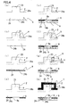
- Each groove 2 preferably has either rectangular contour in a sectional view normal to the longitudinal direction thereof as shown in Fig. 3A, semicircular contour as shown in Fig. 3B, and V-contour as shown in Fig. 3C, because these morphologies can readily be obtained by cutting using a peripheral blade cutting.
- the groove 2 has a rectangular contour in a sectional view normal to the longitudinal direction thereof as shown in Fig. 3A, or V-contour as shown in Fig. 3C
- the contour has two edge portions 2a, 2b abutted with each other as shown in Fig. 3D or Fig. 3E.
- the edge portions 2a and 2b correspond to the side wall and bottom of the groove, respectively, as shown in Fig. 3D, showing an angle of abutment of the both of 90° or around.
- V-formed groove has the edge portions 2a, 2b abutted at an acute angle at the bottom of the groove.
- Degrees of the rounding R1 and R2 are preferably set within a range which ensures a sufficient effect of preventing stress concentration, and which does not ruin effects such as reduction in the series resistance due to groove morphology, where a preferable range is typically 2 to 20 ⁇ m or around.
- the rounding can readily be produced by chemical etching after the grooves are carved by the peripheral blade cutting or the like. The chemical etching may be carried out in common with the etching for removing damage generated during the groove carving. Amount of etching is preferably within a range from 5 to 20 ⁇ m or around so as to make the rounding fall within the above described preferable range.
- Aqueous potassium hydroxide solution is typically used as a chemical etching solution.
- a p-type silicon single crystal ingot which is prepared by adding a Group III element such as gallium to a high-purity silicon, is obtained, and p-type silicon single crystal substrates having a surface orientation of ⁇ 100 ⁇ are sliced out from the ingot.
- the p-type silicon single crystal substrate typically has a specific resistance of 0.5 to 5 ⁇ cm.
- a plurality of parallel grooves of 20 to 100 ⁇ m deep are formed on the first main surface 24a of the p-type ⁇ 100 ⁇ substrate using a high-speed rotary blade in a direction in disagreement with ⁇ 100>, typically in the ⁇ 100> direction.
- the silicon single crystal ingot may be prepared by either of the CZ (Czochralski) method and the FZ (floating zone melting) method, it is more preferably prepared by the CZ method in view of the mechanical strength of the resultant substrate.
- the thickness of the substrate of as small as 40 ⁇ m may ensure a sufficient mechanical strength, the thickness is more preferably 150 ⁇ m or more, and still more preferably 200 ⁇ m or more for the convenience of slicing operation.
- the effect of raising the mechanical strength through adoption of the groove morphology specific to this invention becomes distinctive when a substrate as thin as 230 ⁇ m or below is adopted.
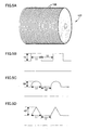
- Fig. 5A shows a schematic view of a high-speed rotary blade 107.
- the high-speed rotary blade 107 comprises a cylindrical portion (e.g., 103 mm in diameter, 165 mm in length) and a plurality of (e.g., 100 to 200) peripheral cutting edges 108 for groove carving attached thereto.
- Profile of the cutting edge may properly be selected depending on the desired morphology of the groove (see Figs. 3A to 3E) from an edge having a rectangular section as shown in Fig. 5B, an edge having a semicircular section as shown in Fig. 5C, and an edge having an angular section as shown in Fig. 5D.
- Heights 10, 10', 10" of the edges fall within a range from 50 to 100 ⁇ m for example, and widths 11, 11', 11" of the edges and distances 12, 12', 12" of edges are typically several hundred micrometers or around for example, respectively.
- Available blades include diamond blades (such as having the surface thereof uniformly adhered with diamond abrasive grain having a grain size of 5 ⁇ m to 10 ⁇ m).
- the grooves 2 can be curved by cutting the main surface of the substrate 1 using the aforementioned high-speed rotary blade at a cutting speed of approx. 1 to 4 cm per second while injecting a cutting fluid. It is also allowable to use a dicer or a wire saw in place of the high-speed rotary blade.
- a texture structure is then formed on the main surface of the substrate, which is carried out as a surface roughening for reducing the reflection loss, by any publicly-known methods such as anisotropic etching.
- the substrate is cleaned in an acidic aqueous solution such as containing hydrochloric acid, sulfuric acid, nitric acid, hydrofluoric acid, or mixed solution thereof, where cleaning in hydrochloric acid is preferable from the viewpoints of economy and production efficiency.
- an acidic aqueous solution such as containing hydrochloric acid, sulfuric acid, nitric acid, hydrofluoric acid, or mixed solution thereof, where cleaning in hydrochloric acid is preferable from the viewpoints of economy and production efficiency.
- an emitter layer 4 is formed in the surficial portion of the substrate after cleaning.
- Methods of forming the emitter layer may be any of the coating diffusion method using diphosphorus pentaoxide, ion implantation method for directly implanting phosphorus ion, and so forth, but a preferable method from the economical viewpoint is the vapor-phase diffusion method using phosphoryl chloride.
- the n-type emitter layer 4 can be formed by annealing the substrate in a phosphoryl chloride atmosphere at 850°C or around. Thickness of the emitter layer 4 is typically 0.5 ⁇ m or around, and the sheet resistance is within a range from 40 to 100 ⁇ / ⁇ or around. A phosphorus glass formed in the surficial portion of the substrate during the process is removed in a hydrofluoric acid solution.
- a silicon nitride layer 8 is formed as a passivation film on the second main surface 24b.
- the silicon nitride layer 8 can be formed by the CVD (Chemical Vapor Deposition) process. Any of the normal-pressure thermal CVD process, reduced-pressure thermal CVD process, photo CVD process and so forth is applicable herein, where the remote plasma CVD process is particularly preferable for this invention, because the process can proceed at lower temperatures ranging from 350 to 400°C or around, and can reduce the surface recombination speed of the silicon nitride layer 8 to be obtained. It is to be noted that the direct thermal nitridation method is not preferable because the process cannot afford a sufficient thickness of the resultant layer.
- grooves 8a for electrode connection are formed in thus-formed silicon nitride layer 8 so as to reach the underlying p-type silicon single crystal substrate 24 using the high-speed rotary blade similar to that shown in Fig. 5A.
- Profile of the cutting edge is selected from the rectangular form as shown in Fig. 5B, semicircular form as shown in Fig. 5C, and angular form as shown in Fig. 5D depending on a desired sectional form of the grooves.
- an electrode 9 is then formed so as to cover the grooves 8a together with the peripheral silicon nitride layer 8 as shown in process (e) in Fig. 4.
- Electrode material Although silver or copper is available as the electrode material herein, aluminum (including alloys thereof) is most preferable in view of economy and workability. Aluminum can be deposited by either method of sputtering and vacuum evaporation. All processes for forming the electrode on the second main surface 24b side thus complete.
- the silicon oxide film 5 is formed on the first main surface 24a by the thermal oxidation method.
- the silicon oxide film 5 serves as a tunnel insulating film between the electrode 6 on the first main surface 24a and the substrate 24, and preferably has a thickness of 5 ⁇ 30 ⁇ in order to optimize tunneling effect while preventing short-circuiting.
- the silicon oxide film 5 can be formed by any known methods including dry oxidation, wet oxidation, steam oxidation, pyrogenic oxidation, hydrochloric acid oxidation and so forth, and among others, dry oxidation is preferably adopted since the method can ensure a high film quality and easy control of the thickness.
- the electrode 6 is formed on the inner side face (electrode-forming area) of the groove 2 on one side as viewed in the width-wise direction of the groove 2, typically to as thick as approx. 5 ⁇ m by the oblique-angled vacuum evaporation process.
- aluminum including alloys thereof
- the material is not limited thereto, and other metal such as silver, copper or the like can be used.
- the substrate 24 is placed in a vacuum evaporation apparatus so as to incline the principal axis thereof at 70° to 85° away from the referential position, where the referential position is defined as a position where the first main surface 24a is oriented to the evaporation source so that the extending direction of the grooves 2 crosses normal to the evaporation source.
- This placement successfully allows the electrode material to deposit predominantly on the inner side face of the grooves 2 on one side as viewed in the width-wise direction.
- the deposition is preferably effected only after the degree of vacuum in the apparatus reaches to a level as low as 2 ⁇ 10 -5 Pa or below, and the deposition speed is adjusted to 10 ⁇ 15 ⁇ /sec (but not limited thereto).
- the substrate 24 having the electrodes 6 deposited thereon is dipped into an acidic aqueous solution containing hydrochloric acid, sulfuric aid, nitric acid, hydrofluoric acid or mixed solution thereof, to thereby remove the unnecessary portion of the electrode material deposited on the top surfaces of the projected ridges 23 generated between the adjacent grooves 2, 2.
- the removal is preferably proceeded typically in hydrochloric acid solution because an appropriate etching rate is attainable, and because unnecessary compound formation due to reaction with the underlying layer is less likely to occur.
- a bus bar electrode (not shown) is formed by a publicly-known method, and the silicon nitride film 7, which serves as a passivation film and an anti-reflection film, is uniformly formed on the first main surface 24a to a thickness of 600 ⁇ 700 ⁇ typically by the remote plasma CVD process (process (h) in Fig. 4), to thereby complete the final solar cell 1.
- the solar cell of this invention it is also allowable to form a light-receiving-element structure of the OECO solar cell also on the second main surface 24b side of the substrate 24 as shown in Fig. 11, similarly to as on the first main surface 24a side.
- the difference in the directions of formation of the grooves 2 on the second main surface 24b side and of the grooves 2 on the first main surface 24a side successfully results in improved mechanical strength of the solar cell having grooves formed on both main surfaces thereof. It is most preferable to form the grooves 2 so that the direction of formation thereof on the second main surface 24b cross nearly normal to those on the first main surface 24a in view of optimizing the mechanical strength.
- Fig. 6A is a drawing showing an embodiment of a solar cell 201 according to the second aspect of this invention.
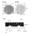
- Fig. 7 is an enlarged schematic sectional view showing a structure on a first main surface 203a side of the solar cell 201.
- a large number of nearly-parallel groove portions 202 of approx. several-hundred-micrometers wide and approx. 100 ⁇ m deep are formed on a first main surface 203a (this surface is defined as the back surface in this embodiment) of a p-type silicon single crystal substrate 203 (also simply referred to as substrate 203), and the groove portions 202 are filled with an electric conductor 205 to thereby form filled electrode lines 240 (Fig. 6A).
- groove portions 202 can be carved en bloc using a set of hundreds to thousands of concentrically-joined rotary blades which rotate all together, where it is also allowable to divide the carving operation into several numbers of run. While the description of this embodiment will be made on a p-type silicon single crystal substrate 203 sliced out from a silicon single crystal ingot, it is to be understood that this invention is by no means limited thereto.
- an insulating film 204 is formed on the first main surface 203a of the p-type silicon single crystal substrate (semiconductor single crystal substrate) 203, and the filled electrode lines 240 are formed so that the electric conductor 205 filled therein makes contact with the p-type silicon single crystal substrate 203 in a form that the groove portions 202 composing the filled electrode lines 240 penetrate the insulating film 204.
- a current collecting electrode communicating with the filled electrode lines 240 is formed on the first main surface 203a, and is preferably formed as a cover electrode layer 210 covering entire surface of the first main surface 203a.
- the insulating film 204 formed on the p-type silicon single crystal substrate 203 may preferably comprise a silicon oxide film, silicon nitride film and the like.
- the first main surface 203a of the p-type silicon single crystal substrate 203 has a surface orientation of ⁇ 100 ⁇ , and the individual groove portions 202 composing the filled electrode lines are formed in the direction in disagreement with the ⁇ 110> direction on the first main surface 203a. This successfully raises the mechanical strength of the solar cell 201. It is to be understood in this specification that any substrate is assumed as having a surface orientation of ⁇ 100 ⁇ if the crystallographic principal axis of the single crystal substrate used herein is an off-angled substrate having an angle of inclination of up to 6° away from the ⁇ 100> direction.
- the first main surface 203a of the ⁇ 100 ⁇ substrate has two ⁇ 110> directions normal to each other, and the direction of formation of the groove portions 202 is set as being in disagreement with both of the ⁇ 110> directions.
- the direction of formation of the groove portions 202 and the direction nearest thereto preferably cross at an angle of 4 ° to 45° on the acute angle side. An angle smaller than 4° may result in only a limited effect of improvement in the mechanical strength of the solar cell 201 as compared with the case where the groove direction agrees with the ⁇ 110> direction. On the other hand, it is geometrically impossible for the angle to exceed 45° away from both of the ⁇ 110> directions.
- the direction of formation of the groove portions 202 becomes most distant from the ⁇ 110> direction, which is a direction of easy cleavage, when it is in parallel with the ⁇ 100> direction on the first main surface 203a (i.e., the above angle equals to 45°), where maximum effect of raising the mechanical strength of the solar cell 201 is attainable.
- a solar cell 201' according to another embodiment of this invention is shown in Fig. 6B, Fig. 10(a) and Fig. 10(b).
- a great number of bottomed holes 214 typically having a diameter of several hundred micrometers and a depth of 5 to 50 ⁇ m or around are formed on a main surface 203a' of a p-type silicon single crystal substrate 203', in a form that every closest bottomed holes 214 are linearly aligned at regular intervals.
- These bottomed holes 214 are filled with an electrode conductor 205' (see Fig. 7), and as a consequence arrays in which every closest bottomed holes 214 are linearly aligned at regular intervals configure filled electrode lines 240'.
- the filled electrode lines 240' are formed so as to penetrate the insulating film 204' as shown in Fig. 7. Assuming now that the direction of a line connecting every closest bottomed holes 214 as the direction of formation of the filled electrode lines 240', such direction of formation of the filled electrode lines 240' is in disagreement with the ⁇ 110> direction on the first main surface 203'.
- the direction of formation of each filled electrode line 240 preferably crosses the ⁇ 110> direction nearest thereto at an angle of 4° to 45° on the acute angle side as shown in Fig.6B, similarly to the case where the filled electrode lines 240 are formed by the aforementioned groove portions 202 (see Fig. 10(a)), and more preferably lies in parallel with the ⁇ 100> direction on the first main surface 203a' (at an angle of 45° to the ⁇ 110> direction).
- a silicon single crystal ingot which is prepared by doping a Group III element such as boron or gallium to a high-purity silicon, is obtained, and p-type silicon single crystal substrates 203 (203') having a surface orientation of ⁇ 100 ⁇ are sliced out from the ingot.
- the p-type silicon single crystal substrate 203 (203') typically has a specific resistivity of 0.5 to 5 ⁇ cm.
- the silicon single crystal ingot may be prepared by either of the CZ (Czochralski) method and the FZ (floating zone melting) method, it is more preferably prepared by the CZ method in view of the mechanical strength of the resultant substrate.
- the effect of raising the mechanical strength through adoption of the groove morphology specific to this invention becomes distinctive when a substrate as thin as 230 ⁇ m or below is adopted.
- a texture structure is then formed by any publicly-known method.
- the substrate is cleaned in an acidic aqueous solution such as containing hydrochloric acid, sulfuric acid, nitric acid, hydrofluoric acid, or mixed solution thereof, where cleaning in hydrochloric acid is preferable from the viewpoints of economy and production efficiency. Purpose of the texture formation resides in surface roughening for reducing the reflection loss.
- the p-type silicon single crystal substrate 203 (203') after completion of the above processes is expressed by process (a) in Fig. 8.
- an insulating film 204 (204') such as a silicon oxide film or silicon nitride film is formed by any publicly-known method, which is typified by the CVD (Chemical Vapor Deposition) process, to a thickness of 50 to 500 nm (process (b) in Fig. 8).
- any of the normal -pressure thermal CVD process, reduced-pressure thermal CVD process, photo CVD process and so forth is applicable herein, where the remote plasma CVD process is particularly preferable for this invention, because the process can proceed at lower temperatures ranging from 350 to 400 °C or around, and can reduce the surface recombination speed of the resultant insulating film 204 (204') comprising silicon oxide or silicon nitride.
- the second main surface (defined as the top surface in this embodiment, although not shown) is used as the light-receiving surface
- the n-type emitter layer can be formed by annealing the p-type silicon single crystal substrate in a phosphoryl chloride atmosphere at 850 °C or around. Thickness of the resultant emitter layer is typically 0.5 ⁇ m or around, and the sheet resistance falls within a range from 40 to 100 ⁇ / ⁇ or around. A phosphorus glass formed in the surficial portion of the substrate during the process is removed in a hydrofluoric acid solution.
- the n-type emitter layer is thus formed in the surficial portion of the second main surface (top surface) which serves as the light-receiving surface, and a p-n junction portion is thus formed in the substrate.
- the filled electrode lines 240 (240') on the first main surface 203a (203a') of the p-type silicon single crystal substrate 203 (203').
- the filled electrode lines 240 are formed by first forming the grooves 202, a plurality of nearly-parallel groove portions are formed on the main surface 203a of the p-type silicon single crystal substrate 203 using a high-speed rotary blade, and by filling the groove portions 202 with the electric conductor 205 (processes (c) and (d) in Fig. 8). More specifically, the groove portions 202 for electrode contact are formed in the insulating layer 204.
- the groove portions 202 are carved typically in the ⁇ 100> direction on the first main surface 203a of the substrate 203, using the high-speed rotary blade 107 as shown in Fig. 5A. Height and profile of the peripheral cutting edge 108 of the high-speed rotary blade 107 can properly be selected depending on desired morphology of the groove portions 202 to be formed on the first main surface 203a of the p-type silicon single crystal substrate 203. Height of the cutting edge is typically 50 to 100 ⁇ m, and width (corresponds with the width of the groove portions 202 to be formed) and pitch (corresponded with the pitch of the groove portions 202 to be formed) are several-hundred-micrometers or around, respectively.
- the substrate is carved at a cutting speed of approx. 1 to 4 cm per second while injecting a cutting water, to thereby form the groove portions 202.
- the height and so forth of the peripheral cutting edge 108 are finely adjusted so as to adjust the depth of the groove portions 202 to approx. 5 to 50 ⁇ m. Because the thickness of the insulating film 204 formed on the first main surface 203a of the substrate 203 is approx. 50 to 500 nm, the groove portions 202 formed in the thickness within the above range can penetrate the insulating film 204. This successfully completes the filled electrode lines 240 in which the electric conductor 205 filled in the groove portions 202 contacts with the p-type silicon single crystal substrate 203.
- the bottomed holes 214 are first linearly formed at regular intervals on the main surface 203a' side of the p-type silicon single crystal substrate 203' by irradiating laser thereon, so that the line connecting every closest bottomed holes 214 is in disagreement with the ⁇ 110> direction.
- the bottomed holes 214 are then filled with the electric conductor 205' for composing the electrodes, to thereby complete the filled electrode lines 240'.
- Lasers available for forming the bottomed holes 214 include carbon dioxide gas laser, argon laser, YAG laser, ruby laser and excimer laser.
- excimer laser such as KrF laser and Nd:YAG laser can preferably be used because these lasers can ensure fine processing to as fine as wavelength of the laser beam, and the processing can be proceeded in the air.
- Any morphology of circular form and rectangular form are allowable for the bottomed holes 214.
- the bottomed holes 214 are linearly aligned while keeping regular intervals between every closest bottomed hole 214.
- a set of thus-linearly-aligned bottomed holes 214 composes one filled electrode line 240', a plurality of the filled electrode lines 240' are periodically arranged on the first main surface 203a' while keeping regular intervals therebetween.
- Fig. 9 is a schematic drawing showing a relation between arrangement of the bottomed holes 214 and directionality of the substrate.
- the direction 212 of a line connecting every closest bottomed holes 214 formed by laser irradiation (direction of formation of the filled electrode line 240') is set in a direction in disagreement with the ⁇ 110> direction on the main surface of the substrate 203'. It is preferable that also the direction 213 of a line connecting every second-closest bottomed hole, differing from the direction 212, is in disagreement with the ⁇ 110> direction.
- Conditions for the laser irradiation for forming the bottomed holes 214 can properly be determined depending on types of the laser, thickness of the insulating film 204', diameter of the bottomed holes 214, and so forth.
- the frequency is preferably within a range from 1 Hz to 100 kHz, and the laser preferably has an average output of 10 mW to 1 kW. Because the insulating film 204' formed herein has a thickness of 50 to 500 nm, it is necessary to irradiate laser having an output energy large enough to remove the insulating film 204' having at least the above-described thickness.
- the filled electrode lines 240 (240') are thus formed by filling the groove portions 202 or bottomed holes 214 with the electric conductor 205 (205'), and the cover electrode layer 210 is formed in a thickness of 0.5 to 2 ⁇ m over the entire portion of the first main surface 203a (203a') (process (d) in Fig. 8).
- the electric conductor 205 (205') and cover electrode layer 210 are successively formed in the same process step, as being started from the status expressed by process (c) in Fig. 8.
- the electric conductor 205 (205') and cover electrode layer 210 can be composed of metals such as silver, copper and the like, or conductive indium oxide, tin oxide and the like, most preferable material is aluminum in view of economy and workability.
- the electric conductor 205 (205') and cover electrode layer 210 can be deposited by any known methods of sputtering, vacuum evaporation, screen printing and so forth.
- the cover electrode layer 210 can, of course, be deposited by uniformly over the entire portion of the first main surface 203 (203') as described in the above, it is also allowable to form a linear or band-formed current collecting electrode 217 (also referred to as band electrode 217, hereinafter) on the filled electrode line 240' which is formed by filling the grooves (not shown) or bottomed holes 14 with the electric conductor 5' as shown in Figs. 10A and 10B typically using a mask for electrode formation. It is also allowable to form the current collecting electrode 217 having a linear form or band form in a direction at 4 to 90° away from the direction of formation of the filled electrode line 240'.
- a linear or band-formed current collecting electrode 217 also referred to as band electrode 217, hereinafter
- FIG. 10(a) and 10(b) showed the case where the filled electrode lines 240' were composed of the bottomed holes 214, the similar current collecting electrode 217 as described in the above can be formed also for the case where the filled electrode lines 240 are composed of the grooves 202.
- the anti-reflection film and electrodes are formed on the second main surface according to the publicly-known methods.
- Materials for composing the anti-reflection film include silicon oxide, silicon nitride, cerium oxide, alumina, tin dioxide, titanium dioxide, magnesium fluoride, tantalum oxide, and a double-layered film composed of any two of these materials, where all materials are available without any problems.
- the anti-reflection film can be formed by the PVD process, CVD process or the like, where any process is successful.
- the anti-reflection film In view of obtaining a high-conversion-efficiency solar cell, it is preferable to compose the anti-reflection film with a silicon nitride film formed by the remote-plasma CVD process, because thus-formed film has a small surface recombination speed.
- the electrodes on the second main surface (top surface) are formed by vacuum evaporation, plating, printing or the like. Although any of these methods are available, printing is preferably used in pursuit of a low cost and high throughput. Typical screen printing uses a silver paste composed of silver powder, glass frit and organic binder mixed with each other, and the electrodes can be formed by annealing the printed paste.
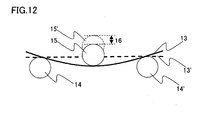
- Each solar cell was cut into a test strip of 18 mm wide and 100 mm long using a dicer.
- solar cells were fabricated using the silicon single crystal substrates having the individual thickness without forming the grooves, but by similarly carrying out etching for damage removal, texture formation, phosphorus diffusion, electrode formation using aluminum on the second main surface, and deposition of the silicon nitride film on the first main surface.
- the solar cells were then similarly subjected to the deflection measurement.
- the test pieces herein were cut out from the substrate so that the longitudinal direction thereof was in agreement with the ⁇ 100> direction of the substrate. Therefore, the axial direction of the round-rod support members 14, 14' herein becomes in parallel with the ⁇ 100> direction normal to another ⁇ 100> direction that lies in parallel with the longitudinal direction of the test piece.
- Fig. 13 shows a groove direction dependence of deflection of the 150- ⁇ m thick substrate. The curve indicates that the deflection becomes maximum when the groove direction is at 45° away from the ⁇ 110> direction, that is, when the grooves are formed in the ⁇ 100> direction, showing an excellent mechanical strength.
- Fig. 14 shows substrate thickness dependences of deflection in comparison with Comparative Example (no grooves). The results indicate that the deflection increases as the thickness of the substrate decreases, and effect of improving the mechanical strength through adjustment of the groove direction becomes more distinctive as the OECO solar cells are thinned. It is also found that the groove formation results in a larger deflection, and that the grooved substrate is more excellent in the mechanical strength.
- first main surfaces of the ⁇ 100 ⁇ p-type silicon single crystal substrates respectively having either thickness of 250, 200 and 150 ⁇ m parallel grooves having a rectangular section were formed respectively in either direction at angles of 0° and 45° to the ⁇ 110> direction by a method similar to as described in Example 1, and on the second main surfaces thereof, a plurality of grooves having a rectangular section were formed normal to the direction of formation of the grooves on the first main surface. Width, depth and pitch of the grooves were determined as 450 ⁇ m, 50 ⁇ m and 600 ⁇ m, respectively.
- the light-receiving element structures were formed on both main surfaces according to the method explained with reference to Fig. 4, to thereby fabricate a double-face-receiving-type OECO solar cell.
- FIG. 11 A schematic view of thus fabricated solar cell was shown in Fig. 11. Test pieces were cut out from these solar cells similarly to as described in Example 1, and subjected to the deflection measurement. Each test pieces was prepared so that the longitudinal direction thereof was in agreement with the groove direction on the first main surface side, and, during the measurement, was disposed so that the groove direction on the first main surface side was in parallel with the round-rod support members 14, 14'.
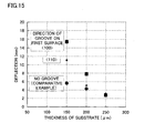
- Fig. 15 shows substrate thickness dependences of the deflection in comparison with Comparative Example. It was found that the deflection became maximum when the grooves were formed in the ⁇ 100> direction and increased as the thickness of the substrate decreased, and an effect of improving the mechanical strength became more distinctive as the OECO solar cells were thinned.
- Aluminum was then deposited over the entire portion of the first main surface to thereby form a back electrode.
- the emitter layer, anti-reflection film, finger electrode and bus bar electrode were sequentially formed by the publicly-known methods, to thereby complete single-face-receiving-type solar cells. Conversion efficiencies of these solar cells were found to range from 15 to 17%.
- Fig. 16 shows groove direction dependence of the deflection. The results indicate that the deflection becomes maximum when the groove direction is at 45° away from the ⁇ 110> direction, that is, when the grooves are formed in the ⁇ 100> direction, showing an excellent mechanical strength.
- a silicon nitride film of 100 nm thick was formed, and a plurality of bottomed holes were formed using KrF excimer laser so that every closest bottomed holes are linearly aligned at regular intervals.
- Distance between the adjacent bottomed holes and diameter of the opening portion were set to 600 ⁇ m and 450 ⁇ m, respectively, and depth of the bottomed holes was set to approx.
- the emitter layer, anti-reflection film, finger electrode and bus bar electrode were sequentially formed by the publicly-known methods, to thereby complete single-face-receiving-type solar cells. Conversion efficiencies of these solar cells were found to range from 14 to 17%.
- Fig. 17 shows ⁇ dependence of the deflection. The results indicate that the deflection becomes maximum when the groove direction is at around 30° and 60° away from the ⁇ 110> direction, that is, when the line connecting every closest bottomed hole is in disagreement with the ⁇ 110> direction, showing an excellent mechanical strength.
Landscapes
- Photovoltaic Devices (AREA)
Abstract
Description
Claims (19)
- A solar cell configured so as to have a plurality of grooves nearly parallel with each other formed on a first main surface of a semiconductor single crystal substrate having a surface orientation of nearly {100}, each of the grooves having an electrode for extracting output disposed on the inner side face thereof on one side in the width-wise direction thereof, and the grooves being formed on the first main surface in directions in disagreement with the <110> direction.
- The solar cell as claimed in Claim 1, wherein the direction of formation of each groove crosses the <110> direction nearest to the direction of formation at an angle of 4° to 45° on the acute angle side.
- The solar cell as claimed in Claim 2, wherein each of the grooves is formed in a direction parallel to the <100> direction on the first main surface.
- The solar cell as claimed in any one of Claims 1 to 3, wherein a contour of each of the grooves in a sectional view normal to the longitudinal direction thereof has any one of rectangular, V- and semicircular forms.
- The solar cell as claimed in any one of Claims 1 to 4, wherein a contour of each of the grooves in a sectional view normal to the longitudinal direction thereof has two edge portions abutted with each other, and the abutted portion of the edge portions is rounded.
- The solar cell as claimed in any one of Claims 1 to 5, configured so that a plurality of grooves nearly parallel with each other are formed also on a second main surface of the semiconductor single crystal substrate in directions in disagreement with the <110> direction on the first main surface and so as to cross the directions of formation of the grooves on the first main surface, and so that an electrode for extracting output is disposed on the inner side face of each groove on the second main surface on one side in the width-wise direction of the groove.
- The solar cell as claimed in Claim 6, wherein the directions of formation of the grooves on the second main surface cross nearly normal to the directions of formation of the grooves on the first main surface.
- A solar cell configured so as to have a plurality of filled electrode lines, having an electric conductor for composing electrodes for extracting output filled therein, on at least either main surface side of a semiconductor single crystal substrate having a surface orientation of nearly {100}, the filled electrode lines being formed in directions in disagreement with the <110> direction on the main surface.
- The solar cell as claimed in Claim 8, wherein the direction of formation of each filled electrode line crosses the <110> direction nearest to the direction of formation at an angle of 4 ° to 45° on the acute angle side.
- The solar cell as claimed in Claim 8 or 9, wherein each of the grooves is formed in a direction parallel to the <100> direction on the main surface.
- The solar cell as claimed in any one of Claims 8 to 10, wherein the filled electrode lines are formed on the first main surface of the semiconductor single crystal substrate, and the second main surface serves as a light-receiving surface.
- The solar cell as claimed in Claim 11, wherein an insulating film is formed on the first main surface of the semiconductor single crystal substrate, and the filled electrode lines are formed so that the electric conductor filled therein makes contact with the semiconductor single crystal substrate in a form that the filled electrode lines penetrate the insulating film.
- The solar cell as claimed in Claim 12, wherein a current collecting electrode communicating with the filled electrode lines formed on the first main surface is formed again on the first main surface.
- The solar cell as claimed in Claim 13, wherein the current collecting electrode is a cover electrode layer covering entire portion of the first main surface.
- The solar cell as claimed in Claim 13, wherein the current collecting electrode is formed so as to have a band pattern or line pattern on the filled electrode lines.
- The solar cell as claimed in Claim 13, wherein the current collecting electrode is formed so as to have a band pattern or line pattern, and in the direction inclined at 4° to 90° away from the direction of formation of the filled electrode lines.
- A method of fabricating a solar cell comprising a step of forming a plurality of filled electrode lines, having an electric conductor for composing electrodes for extracting output filled therein, on at least either main surface side of a semiconductor single crystal substrate having a surface orientation of nearly {100}, in directions in disagreement with-the <110> direction on the main surface.
- The method of fabricating a solar cell as claimed in Claim 17, wherein the filled electrode lines are formed by first forming a plurality of groove portions nearly parallel with each other on the main surface of the semiconductor single crystal substrate, and then by filling the groove portions with the electric conductor for composing electrodes.
- The method of fabricating a solar cell as claimed in Claim 17, wherein the filled electrode lines are formed by first forming a plurality of bottomed holes on the main surface of the semiconductor single crystal substrate by laser irradiation, the bottomed holes being linearly aligned at regular intervals, and the direction of a line connecting every closest bottomed holes being in disagreement with the <110> direction, and then by filling the groove portions with the electric conductor for composing electrodes.
Applications Claiming Priority (7)
| Application Number | Priority Date | Filing Date | Title |
|---|---|---|---|
| JP2001024240 | 2001-01-31 | ||
| JP2001024240 | 2001-01-31 | ||
| JP2001052285 | 2001-02-27 | ||
| JP2001052285A JP4149678B2 (en) | 2001-01-31 | 2001-02-27 | Solar cell |
| JP2001071610A JP3872305B2 (en) | 2001-03-14 | 2001-03-14 | Solar cell and manufacturing method thereof |
| JP2001071610 | 2001-03-14 | ||
| PCT/JP2002/000702 WO2002061851A1 (en) | 2001-01-31 | 2002-01-30 | Solar cell and method for producing the same |
Publications (2)
| Publication Number | Publication Date |
|---|---|
| EP1365455A1 true EP1365455A1 (en) | 2003-11-26 |
| EP1365455A4 EP1365455A4 (en) | 2006-09-20 |
Family
ID=27345872
Family Applications (1)
| Application Number | Title | Priority Date | Filing Date |
|---|---|---|---|
| EP02711237A Ceased EP1365455A4 (en) | 2001-01-31 | 2002-01-30 | SOLAR CELL AND METHOD FOR THE PRODUCTION THEREOF |
Country Status (5)
| Country | Link |
|---|---|
| US (1) | US7294779B2 (en) |
| EP (1) | EP1365455A4 (en) |
| KR (1) | KR100831291B1 (en) |
| CN (1) | CN1274032C (en) |
| WO (1) | WO2002061851A1 (en) |
Cited By (1)
| Publication number | Priority date | Publication date | Assignee | Title |
|---|---|---|---|---|
| DE102004053873A1 (en) * | 2004-11-07 | 2006-05-11 | Institut Für Solarenergieforschung Gmbh | Process for the preparation of a double-sided light-sensitive solar cell and a photosensitive solar cell on both sides |
Families Citing this family (59)
| Publication number | Priority date | Publication date | Assignee | Title |
|---|---|---|---|---|
| JP3872306B2 (en) * | 2001-02-01 | 2007-01-24 | 信越半導体株式会社 | Solar cell module and method for installing solar cell module |
| US20050189015A1 (en) * | 2003-10-30 | 2005-09-01 | Ajeet Rohatgi | Silicon solar cells and methods of fabrication |
| CN100521252C (en) * | 2004-09-03 | 2009-07-29 | 信越化学工业株式会社 | Module for solar power generation and solar power generation system using same |
| US7790574B2 (en) | 2004-12-20 | 2010-09-07 | Georgia Tech Research Corporation | Boron diffusion in silicon devices |
| US20090112197A1 (en) | 2007-10-30 | 2009-04-30 | Searete Llc | Devices configured to facilitate release of nitric oxide |
| US8642093B2 (en) | 2007-10-30 | 2014-02-04 | The Invention Science Fund I, Llc | Methods and systems for use of photolyzable nitric oxide donors |
| US8221690B2 (en) | 2007-10-30 | 2012-07-17 | The Invention Science Fund I, Llc | Systems and devices that utilize photolyzable nitric oxide donors |
| US7862598B2 (en) | 2007-10-30 | 2011-01-04 | The Invention Science Fund I, Llc | Devices and systems that deliver nitric oxide |
| US20090025786A1 (en) * | 2007-05-07 | 2009-01-29 | Georgia Tech Research Corporation | Solar cell having high quality back contact with screen-printed local back surface field |
| US20090308442A1 (en) * | 2008-06-12 | 2009-12-17 | Honeywell International Inc. | Nanostructure enabled solar cell electrode passivation via atomic layer deposition |
| GB0719554D0 (en) * | 2007-10-05 | 2007-11-14 | Univ Glasgow | semiconductor optoelectronic devices and methods for making semiconductor optoelectronic devices |
| US8877508B2 (en) | 2007-10-30 | 2014-11-04 | The Invention Science Fund I, Llc | Devices and systems that deliver nitric oxide |
| US8980332B2 (en) | 2007-10-30 | 2015-03-17 | The Invention Science Fund I, Llc | Methods and systems for use of photolyzable nitric oxide donors |
| US10080823B2 (en) | 2007-10-30 | 2018-09-25 | Gearbox Llc | Substrates for nitric oxide releasing devices |
| US7846400B2 (en) | 2007-10-30 | 2010-12-07 | The Invention Science Fund I, Llc | Substrates for nitric oxide releasing devices |
| US7897399B2 (en) | 2007-10-30 | 2011-03-01 | The Invention Science Fund I, Llc | Nitric oxide sensors and systems |
| US8481357B2 (en) * | 2008-03-08 | 2013-07-09 | Crystal Solar Incorporated | Thin film solar cell with ceramic handling layer |
| TWI366252B (en) * | 2008-08-06 | 2012-06-11 | Jer Liang Yeh | Substrate with high fracture strength, structure for increasing the fracture strength of a substrate and the method thereof |
| KR101010286B1 (en) | 2008-08-29 | 2011-01-24 | 엘지전자 주식회사 | Manufacturing method of solar cell |
| US8384007B2 (en) * | 2009-10-07 | 2013-02-26 | Zena Technologies, Inc. | Nano wire based passive pixel image sensor |
| US8299472B2 (en) * | 2009-12-08 | 2012-10-30 | Young-June Yu | Active pixel sensor with nanowire structured photodetectors |
| US8274039B2 (en) * | 2008-11-13 | 2012-09-25 | Zena Technologies, Inc. | Vertical waveguides with various functionality on integrated circuits |
| US8546742B2 (en) | 2009-06-04 | 2013-10-01 | Zena Technologies, Inc. | Array of nanowires in a single cavity with anti-reflective coating on substrate |
| US9478685B2 (en) | 2014-06-23 | 2016-10-25 | Zena Technologies, Inc. | Vertical pillar structured infrared detector and fabrication method for the same |
| US8507840B2 (en) | 2010-12-21 | 2013-08-13 | Zena Technologies, Inc. | Vertically structured passive pixel arrays and methods for fabricating the same |
| US20100148221A1 (en) * | 2008-11-13 | 2010-06-17 | Zena Technologies, Inc. | Vertical photogate (vpg) pixel structure with nanowires |
| US9299866B2 (en) * | 2010-12-30 | 2016-03-29 | Zena Technologies, Inc. | Nanowire array based solar energy harvesting device |
| US8735797B2 (en) | 2009-12-08 | 2014-05-27 | Zena Technologies, Inc. | Nanowire photo-detector grown on a back-side illuminated image sensor |
| US8748799B2 (en) | 2010-12-14 | 2014-06-10 | Zena Technologies, Inc. | Full color single pixel including doublet or quadruplet si nanowires for image sensors |
| US8890271B2 (en) | 2010-06-30 | 2014-11-18 | Zena Technologies, Inc. | Silicon nitride light pipes for image sensors |
| US8229255B2 (en) * | 2008-09-04 | 2012-07-24 | Zena Technologies, Inc. | Optical waveguides in image sensors |
| US9515218B2 (en) * | 2008-09-04 | 2016-12-06 | Zena Technologies, Inc. | Vertical pillar structured photovoltaic devices with mirrors and optical claddings |
| US8519379B2 (en) | 2009-12-08 | 2013-08-27 | Zena Technologies, Inc. | Nanowire structured photodiode with a surrounding epitaxially grown P or N layer |
| US8269985B2 (en) | 2009-05-26 | 2012-09-18 | Zena Technologies, Inc. | Determination of optimal diameters for nanowires |
| US8866065B2 (en) | 2010-12-13 | 2014-10-21 | Zena Technologies, Inc. | Nanowire arrays comprising fluorescent nanowires |
| US9000353B2 (en) | 2010-06-22 | 2015-04-07 | President And Fellows Of Harvard College | Light absorption and filtering properties of vertically oriented semiconductor nano wires |
| US8835831B2 (en) | 2010-06-22 | 2014-09-16 | Zena Technologies, Inc. | Polarized light detecting device and fabrication methods of the same |
| US8791470B2 (en) | 2009-10-05 | 2014-07-29 | Zena Technologies, Inc. | Nano structured LEDs |
| US9406709B2 (en) | 2010-06-22 | 2016-08-02 | President And Fellows Of Harvard College | Methods for fabricating and using nanowires |
| US9343490B2 (en) | 2013-08-09 | 2016-05-17 | Zena Technologies, Inc. | Nanowire structured color filter arrays and fabrication method of the same |
| US8889455B2 (en) * | 2009-12-08 | 2014-11-18 | Zena Technologies, Inc. | Manufacturing nanowire photo-detector grown on a back-side illuminated image sensor |
| US9082673B2 (en) | 2009-10-05 | 2015-07-14 | Zena Technologies, Inc. | Passivated upstanding nanostructures and methods of making the same |
| US20110168263A1 (en) * | 2008-09-18 | 2011-07-14 | The Regents Of The University Of California | Design of higher efficiency silicon solar cells |
| US7816239B2 (en) * | 2008-11-20 | 2010-10-19 | Varian Semiconductor Equipment Associates, Inc. | Technique for manufacturing a solar cell |
| US20100186808A1 (en) * | 2009-01-27 | 2010-07-29 | Peter Borden | Plating through tunnel dielectrics for solar cell contact formation |
| DE102009022318A1 (en) * | 2009-05-22 | 2010-12-23 | Schott Solar Ag | Method for producing a photovoltaic module |
| KR101146737B1 (en) * | 2009-06-29 | 2012-05-18 | 엘지전자 주식회사 | Solar cell and method for manufacturing the same |
| US20150004366A1 (en) * | 2009-08-03 | 2015-01-01 | National Tsing Hua University | Substrate with high fracture strength |
| US9991407B1 (en) * | 2010-06-22 | 2018-06-05 | Banpil Photonics Inc. | Process for creating high efficiency photovoltaic cells |
| DE102010025968B4 (en) * | 2010-07-02 | 2016-06-02 | Schott Ag | Generation of microholes |
| CN103733352A (en) * | 2011-06-13 | 2014-04-16 | Posco公司 | Solar cell substrate and solar cell using same |
| US8960657B2 (en) | 2011-10-05 | 2015-02-24 | Sunedison, Inc. | Systems and methods for connecting an ingot to a wire saw |
| TWI467783B (en) * | 2011-11-10 | 2015-01-01 | Nat Univ Tsing Hua | A solar cell manufacturing method and solar cell with curved embedded electrode wire |
| CN103137781B (en) * | 2011-11-30 | 2016-11-23 | 江苏艾德太阳能科技有限公司 | The manufacture method of the solaode of tool bending buried electrode line and this solaode |
| EP2693487A3 (en) * | 2012-07-31 | 2014-07-30 | Samsung SDI Co., Ltd. | Thin film solar cell module and method of manufacturing the same |
| TWI636577B (en) * | 2013-02-07 | 2018-09-21 | 茂迪股份有限公司 | Solar cell and its module |
| DE102013109143A1 (en) * | 2013-08-23 | 2015-02-26 | Nts Nanotechnologysolar | Photocell, in particular solar cell and method for producing a photocell |
| CN105575761B (en) * | 2014-10-13 | 2018-07-10 | 北大方正集团有限公司 | The manufacturing method and slot type power device of slot type power device |
| CN109216479A (en) * | 2018-09-07 | 2019-01-15 | 泰州隆基乐叶光伏科技有限公司 | A kind of solar battery and its production technology |
Family Cites Families (17)
| Publication number | Priority date | Publication date | Assignee | Title |
|---|---|---|---|---|
| FR2489597A1 (en) * | 1980-08-29 | 1982-03-05 | Radiotechnique Compelec | SOLAR CELL WITH PHOTOSENSITIVE FACE RAINUREE |
| US4379944A (en) * | 1981-02-05 | 1983-04-12 | Varian Associates, Inc. | Grooved solar cell for deployment at set angle |
| US4626613A (en) * | 1983-12-23 | 1986-12-02 | Unisearch Limited | Laser grooved solar cell |
| JPS60167509A (en) * | 1984-02-10 | 1985-08-30 | Toshiba Corp | Production of surface acoustic wave element |
| US4608451A (en) * | 1984-06-11 | 1986-08-26 | Spire Corporation | Cross-grooved solar cell |
| DE3712503A1 (en) | 1987-04-13 | 1988-11-03 | Nukem Gmbh | SOLAR CELL |
| US5011565A (en) | 1989-12-06 | 1991-04-30 | Mobil Solar Energy Corporation | Dotted contact solar cell and method of making same |
| JPH03288476A (en) | 1990-04-03 | 1991-12-18 | Sharp Corp | Semiconductor device |
| DE4033658A1 (en) | 1990-10-23 | 1992-04-30 | Siemens Ag | METHOD FOR PROCESSING TRENCH FLANKES IN SEMICONDUCTOR SUBSTRATES |
| US5356488A (en) * | 1991-12-27 | 1994-10-18 | Rudolf Hezel | Solar cell and method for its manufacture |
| EP0742959B1 (en) | 1993-07-29 | 2001-11-14 | Gerhard Willeke | Method of producing a solar cell and solar cell produced using this method |
| JPH08213348A (en) | 1995-02-03 | 1996-08-20 | Yamaha Corp | Dividing method of crystal wafer |
| JP3070912B2 (en) | 1997-03-18 | 2000-07-31 | 株式会社日立製作所 | Solar cell |
| DE19741832A1 (en) | 1997-09-23 | 1999-03-25 | Inst Solarenergieforschung | Method of manufacturing a solar cell and solar cell |
| US6452091B1 (en) * | 1999-07-14 | 2002-09-17 | Canon Kabushiki Kaisha | Method of producing thin-film single-crystal device, solar cell module and method of producing the same |
| JP4149678B2 (en) | 2001-01-31 | 2008-09-10 | 信越半導体株式会社 | Solar cell |
| US7355114B2 (en) * | 2001-03-19 | 2008-04-08 | Shin-Etsu Handotai Co., Ltd. | Solar cell and its manufacturing method |
-
2002
- 2002-01-30 EP EP02711237A patent/EP1365455A4/en not_active Ceased
- 2002-01-30 US US10/470,242 patent/US7294779B2/en not_active Expired - Lifetime
- 2002-01-30 KR KR1020037009945A patent/KR100831291B1/en not_active Expired - Lifetime
- 2002-01-30 CN CNB028043731A patent/CN1274032C/en not_active Expired - Lifetime
- 2002-01-30 WO PCT/JP2002/000702 patent/WO2002061851A1/en not_active Ceased
Cited By (1)
| Publication number | Priority date | Publication date | Assignee | Title |
|---|---|---|---|---|
| DE102004053873A1 (en) * | 2004-11-07 | 2006-05-11 | Institut Für Solarenergieforschung Gmbh | Process for the preparation of a double-sided light-sensitive solar cell and a photosensitive solar cell on both sides |
Also Published As
| Publication number | Publication date |
|---|---|
| CN1274032C (en) | 2006-09-06 |
| US7294779B2 (en) | 2007-11-13 |
| WO2002061851A1 (en) | 2002-08-08 |
| CN1489793A (en) | 2004-04-14 |
| EP1365455A4 (en) | 2006-09-20 |
| KR20030071866A (en) | 2003-09-06 |
| US20040065362A1 (en) | 2004-04-08 |
| KR100831291B1 (en) | 2008-05-22 |
Similar Documents
| Publication | Publication Date | Title |
|---|---|---|
| US7294779B2 (en) | Solar cell and method for producing the same | |
| AU2002238953B2 (en) | Solar cell and its manufacturing method | |
| US7875794B2 (en) | Semiconductor wafer processing to increase the usable planar surface area | |
| US5704992A (en) | Solar cell and method for manufacturing a solar cell | |
| US20080314443A1 (en) | Back-contact solar cell for high power-over-weight applications | |
| EP2618382B1 (en) | Solar cell and manufacturing method thereof | |
| JP5408022B2 (en) | Solar cell and manufacturing method thereof | |
| JP3872305B2 (en) | Solar cell and manufacturing method thereof | |
| JP4378485B2 (en) | Manufacturing method of solar cell | |
| JP2005327871A (en) | Solar cell and manufacturing method thereof | |
| JP4431712B2 (en) | Manufacturing method of solar cell | |
| US7994064B2 (en) | Selective etch for damage at exfoliated surface | |
| AU2007202916A1 (en) | Solar Cell |
Legal Events
| Date | Code | Title | Description |
|---|---|---|---|
| PUAI | Public reference made under article 153(3) epc to a published international application that has entered the european phase |
Free format text: ORIGINAL CODE: 0009012 |
|
| 17P | Request for examination filed |
Effective date: 20030822 |
|
| AK | Designated contracting states |
Kind code of ref document: A1 Designated state(s): AT BE CH CY DE DK ES FI FR GB GR IE IT LI LU MC NL PT SE TR |
|
| A4 | Supplementary search report drawn up and despatched |
Effective date: 20060821 |
|
| RIC1 | Information provided on ipc code assigned before grant |
Ipc: H01L 31/0224 20060101AFI20060814BHEP |
|
| RAP1 | Party data changed (applicant data changed or rights of an application transferred) |
Owner name: SHIN-ETSU CHEMICAL CO., LTD. Owner name: SHIN-ETSU HANDOTAI CO., LTD. |
|
| 17Q | First examination report despatched |
Effective date: 20091124 |
|
| REG | Reference to a national code |
Ref country code: DE Ref legal event code: R003 |
|
| STAA | Information on the status of an ep patent application or granted ep patent |
Free format text: STATUS: THE APPLICATION HAS BEEN REFUSED |
|
| 18R | Application refused |
Effective date: 20160621 |