EP1364788A2 - Ink jet print head and method and apparatus for bonding flexible printed circuit cable for ink jet print head - Google Patents
Ink jet print head and method and apparatus for bonding flexible printed circuit cable for ink jet print head Download PDFInfo
- Publication number
- EP1364788A2 EP1364788A2 EP02257528A EP02257528A EP1364788A2 EP 1364788 A2 EP1364788 A2 EP 1364788A2 EP 02257528 A EP02257528 A EP 02257528A EP 02257528 A EP02257528 A EP 02257528A EP 1364788 A2 EP1364788 A2 EP 1364788A2
- Authority
- EP
- European Patent Office
- Prior art keywords
- bonding
- pads
- substrate
- conductors
- fpc cable
- Prior art date
- Legal status (The legal status is an assumption and is not a legal conclusion. Google has not performed a legal analysis and makes no representation as to the accuracy of the status listed.)
- Withdrawn
Links
Images




Classifications
-
- H—ELECTRICITY
- H05—ELECTRIC TECHNIQUES NOT OTHERWISE PROVIDED FOR
- H05K—PRINTED CIRCUITS; CASINGS OR CONSTRUCTIONAL DETAILS OF ELECTRIC APPARATUS; MANUFACTURE OF ASSEMBLAGES OF ELECTRICAL COMPONENTS
- H05K3/00—Apparatus or processes for manufacturing printed circuits
- H05K3/36—Assembling printed circuits with other printed circuits
- H05K3/361—Assembling flexible printed circuits with other printed circuits
-
- B—PERFORMING OPERATIONS; TRANSPORTING
- B41—PRINTING; LINING MACHINES; TYPEWRITERS; STAMPS
- B41J—TYPEWRITERS; SELECTIVE PRINTING MECHANISMS, i.e. MECHANISMS PRINTING OTHERWISE THAN FROM A FORME; CORRECTION OF TYPOGRAPHICAL ERRORS
- B41J2/00—Typewriters or selective printing mechanisms characterised by the printing or marking process for which they are designed
- B41J2/005—Typewriters or selective printing mechanisms characterised by the printing or marking process for which they are designed characterised by bringing liquid or particles selectively into contact with a printing material
- B41J2/01—Ink jet
- B41J2/135—Nozzles
- B41J2/16—Production of nozzles
-
- B—PERFORMING OPERATIONS; TRANSPORTING
- B41—PRINTING; LINING MACHINES; TYPEWRITERS; STAMPS
- B41J—TYPEWRITERS; SELECTIVE PRINTING MECHANISMS, i.e. MECHANISMS PRINTING OTHERWISE THAN FROM A FORME; CORRECTION OF TYPOGRAPHICAL ERRORS
- B41J2/00—Typewriters or selective printing mechanisms characterised by the printing or marking process for which they are designed
- B41J2/005—Typewriters or selective printing mechanisms characterised by the printing or marking process for which they are designed characterised by bringing liquid or particles selectively into contact with a printing material
- B41J2/01—Ink jet
- B41J2/135—Nozzles
- B41J2/14—Structure thereof only for on-demand ink jet heads
- B41J2/14016—Structure of bubble jet print heads
- B41J2/14072—Electrical connections, e.g. details on electrodes, connecting the chip to the outside...
-
- H—ELECTRICITY
- H05—ELECTRIC TECHNIQUES NOT OTHERWISE PROVIDED FOR
- H05K—PRINTED CIRCUITS; CASINGS OR CONSTRUCTIONAL DETAILS OF ELECTRIC APPARATUS; MANUFACTURE OF ASSEMBLAGES OF ELECTRICAL COMPONENTS
- H05K1/00—Printed circuits
- H05K1/02—Details
- H05K1/14—Structural association of two or more printed circuits
- H05K1/147—Structural association of two or more printed circuits at least one of the printed circuits being bent or folded, e.g. by using a flexible printed circuit
-
- H—ELECTRICITY
- H05—ELECTRIC TECHNIQUES NOT OTHERWISE PROVIDED FOR
- H05K—PRINTED CIRCUITS; CASINGS OR CONSTRUCTIONAL DETAILS OF ELECTRIC APPARATUS; MANUFACTURE OF ASSEMBLAGES OF ELECTRICAL COMPONENTS
- H05K2201/00—Indexing scheme relating to printed circuits covered by H05K1/00
- H05K2201/03—Conductive materials
- H05K2201/0332—Structure of the conductor
- H05K2201/0364—Conductor shape
- H05K2201/0367—Metallic bump or raised conductor not used as solder bump
-
- H—ELECTRICITY
- H05—ELECTRIC TECHNIQUES NOT OTHERWISE PROVIDED FOR
- H05K—PRINTED CIRCUITS; CASINGS OR CONSTRUCTIONAL DETAILS OF ELECTRIC APPARATUS; MANUFACTURE OF ASSEMBLAGES OF ELECTRICAL COMPONENTS
- H05K2201/00—Indexing scheme relating to printed circuits covered by H05K1/00
- H05K2201/03—Conductive materials
- H05K2201/0332—Structure of the conductor
- H05K2201/0388—Other aspects of conductors
- H05K2201/0397—Tab
-
- H—ELECTRICITY
- H05—ELECTRIC TECHNIQUES NOT OTHERWISE PROVIDED FOR
- H05K—PRINTED CIRCUITS; CASINGS OR CONSTRUCTIONAL DETAILS OF ELECTRIC APPARATUS; MANUFACTURE OF ASSEMBLAGES OF ELECTRICAL COMPONENTS
- H05K2203/00—Indexing scheme relating to apparatus or processes for manufacturing printed circuits covered by H05K3/00
- H05K2203/01—Tools for processing; Objects used during processing
- H05K2203/0195—Tool for a process not provided for in H05K3/00, e.g. tool for handling objects using suction, for deforming objects, for applying local pressure
-
- H—ELECTRICITY
- H05—ELECTRIC TECHNIQUES NOT OTHERWISE PROVIDED FOR
- H05K—PRINTED CIRCUITS; CASINGS OR CONSTRUCTIONAL DETAILS OF ELECTRIC APPARATUS; MANUFACTURE OF ASSEMBLAGES OF ELECTRICAL COMPONENTS
- H05K3/00—Apparatus or processes for manufacturing printed circuits
- H05K3/30—Assembling printed circuits with electric components, e.g. with resistors
- H05K3/32—Assembling printed circuits with electric components, e.g. with resistors electrically connecting electric components or wires to printed circuits
- H05K3/328—Assembling printed circuits with electric components, e.g. with resistors electrically connecting electric components or wires to printed circuits by welding
Definitions
- the present invention relates to ink jet print heads, methods of bonding a flexible printed circuit (FPC) cable for an ink jet print head, and to apparatus adopting the method.
- FPC flexible printed circuit
- a substrate having heaters and nozzles thereon is included.
- the substrate also includes a plurality of signal lines electrically connected to the heaters, and a plurality of electric pads arranged on the edge of the substrate in an inline configuration in order to achieve the contact of the signal lines and an external circuit.
- the pads are connected to an FPC cable on which a plurality of conductors corresponding to the pads are arranged side by side.
- the pads are bonded to the conductors by thermosonic bonding.
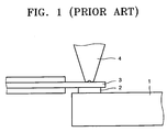
- thermosonic bonding technique corresponds to a single point bonding method of bonding a single point at a time. Accordingly, as shown in Figure 1, in a state where a conductor 3 contacts a pad 2 installed on a substrate 1 and then a thermosonic bonding tool 4 contacts the resultant substrate structure, the pad 2 is bonded to the conductor 3 by one time bonding. In this way, the other pads and conductors are sequentially bonded together. According to this conventional method, as many bonding processes as the number of pads installed on a substrate must be performed, consequently requiring a lot of time to bond an FPC cable to a single substrate.
- the bonding tool partially contacts the conductor upon thermosonic bonding, and hence the contacted portion of the conductor on which vibration energy generated by ultrasonic is focused may be deformed. Accordingly, the rigidity of the contacted portion decreases, so that the conductor may be easily separated from the pad.
- FPC flexible printed circuit
- Another aim of preferred embodiments of the present invention is to provide an ink jet print head, a method of bonding an FPC cable for an ink jet print head, and an apparatus adopting the method, in which the portion where an FPC conductor and a pad are joined together provides an increased structural intensity.
- Still another aim of preferred embodiments of the present invention is to provide an ink jet print head, a method of bonding an FPC cable for an ink jet print head, and an apparatus adopting the method, in which the printing quality is increased by a reduction in the interlaced distance of droplet.
- the present invention provides, in a first aspect, a method of bonding an FPC for an ink jet print head, the method comprising: preparing a substrate for an ink jet print head, the substrate having a plurality of resistive heaters, a plurality of signal lines connected to the resistive heaters, and a plurality of electrical pads for connecting the signal lines to the outside; preparing an FPC cable having a plurality of conductors having bonding portions, the conductors corresponding to the pads; preparing a bonding apparatus adopting a hot pressure welding technique, the bonding apparatus having a stage for mounting the substrate on and a bonding tool for pressing the bonding portions of the conductors down on the pads of the substrate and heating the bonding portions attached to the pads; mounting the substrate on the stage of the bonding apparatus in order to combine the substrate with the FPC cable; arranging the FPC cable on the substrate so that the bonding portions of the conductors face the corresponding pads; and pressing at least two conductors down on the corresponding pads at a time using the
- the present invention provides, in a second aspect, another method of bonding an FPC for an ink jet print head, the method comprising: preparing a substrate for an ink jet print head, the substrate having a plurality of resistive heaters, a plurality of signal lines connected to the resistive heaters, and a plurality of electrical pads for connecting the signal lines to the outside; preparing an FPC cable, the FPC cable having a plurality of conductors having bonding portions facing the pads, an upper protect film completely covering the upper surface of a conductor, and a lower protect film covering the lower surface of the conductor except for the bonding portion facing a pad; preparing a bonding apparatus adopting a hot pressure welding technique, the bonding apparatus having a stage for mounting the substrate on and a bonding tool for pressing the bonding portions of the conductors down on the pads of the substrate and heating the bonding portions attached to the pads; mounting the substrate on the stage of the bonding apparatus in order to combine the substrate with the FPC cable; arranging the FPC cable on the substrate
- a tip for bringing the bonding portion of a conductor in contact with a corresponding pad is formed at both edges of the bonding tool.
- the bonding tool bonds the conductors to the pads
- the pads installed on one edge of the substrate are bonded symmetrically to the pads installed on the other edge of the substrate.
- the bonding tool bonds the conductors to the pads, it bends the FPC cable so that the bent portion of the FPC cable is placed at the rear of the substrate.
- bonding is performed with a bump interposed between the bonding portion of a conductor and a pad.
- the lower protect film has an aperture facing a pad, and a bump is inserted into the aperture and electrically connects the bonding portion of a conductor to a corresponding pad.
- the present invention in a third aspect, provides a bonding apparatus for bonding the bonding portions of an FPC cable to the pads of a substrate in order to electrically connect the substrate for an ink jet print head, the substrate having a plurality of resistive heaters, a plurality of signal lines connected to the resistive heaters, and a plurality of electrical pads for connecting the signal lines to the outside, to the FPC cable having a plurality of conductors having bonding portions facing the pads, the bonding apparatus comprising a stage on which the substrate is mounted with the pads facing upward, and a bonding tool that moves up and down over the stage and has a bonding tip for pressing at least two bonding portions down on the corresponding pads and heating the bonding portions in contact with the pads to thereby bond the bonding portion to the pads using a hot pressure welding technique.
- the bonding tool has a tip for bringing the bonding portions of the conductors of the FPC cable in contact with corresponding pads. More preferably, the tip protrudes from both edges of the bonding tool in order to bond opposite conductors to corresponding opposite pads among the pads formed on both edges of the substrate.
- the bonding tool has a dam-shaped tip that covers all of the pads formed on the substrate. Also, the dam-shaped tip is symmetrically formed at both ends of the bonding tool such that the dam-shaped tip covers all of the pads formed along both edges of the substrate. Furthermore, the bonding tool has a protruding extension for bending the FPC cable beside the each edge of the substrate so that the FPC cable is placed from the upper surface level of the substrate to the position at the rear of the substrate.
- the present invention in a fourth aspect, provides an ink jet print head comprising a substrate having a plurality of resistive heaters, a plurality of signal lines connected to the resistive heaters, and a plurality of electrical pads for connecting the signal lines to an external circuit; and an FPC cable having a plurality of conductors and upper and lower films for protecting a conductor, wherein each of the conductors has a bonding portion to be bonded to a corresponding pad, wherein the conductors of the FPC cable are bonded to the corresponding pads of the substrate by hot pressure welding, and the bonding portion of a conductor that faces a corresponding pad is covered by the upper and lower films.
- the FPC cable is bent such that its bent portion is placed at the rear of the substrate. It is also preferable that the upper and lower surfaces of a conductor is covered by the upper and lower films, and the lower film has a window formed directly over a corresponding pad to allow the conductor to contact the pad.
- a conductive bump is interposed between the bonding portion of a conductor and a corresponding pad.
- Preferred embodiments of the present invention basically adopt hot pressure welding instead of thermosonic bonding, that is, thermosonic welding using local kinetic energy.
- thermosonic welding using local kinetic energy.
- a fragile substrate is not subject to vibration impact, so that simultaneous bonding with respect to several pads is possible in contrast with thermosonic bonding.
- FIG. 2 is a flowchart for illustrating a bonding method according to an embodiment of the present invention.
- a substrate for an ink jet print head is prepared, in step 91.
- a flexible printed circuit (FPC) cable to be bonded to the substrate is prepared, in step 92.
- a bonding apparatus for bonding the conductors of the FPC cable to the pads on the substrate using the hot pressure welding technique is prepared, in step 93.
- the substrate is mounted on the stage of the bonding apparatus, in step 94.
- the FPC cable is arranged on the substrate, in step 95.
- the bonding tool of the bonding apparatus bonds the conductors of the FPC cable to the pads on the substrate using the hot pressure welding technique, in step 96. At this time, at least two conductors are bonded to at least two pads. This bonding repeats until all of the pads on the substrate are bonded to the corresponding conductors, in step 97. However, all of the pads can be simultaneously bonded to the corresponding conductors at a time.
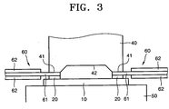
- FIG 3 is a schematic structure diagram of a bonding apparatus according to an embodiment of the present invention in which a bonding tool bonds an FPC cable to a substrate in a bonding method according to a first embodiment of the present invention.
- a substrate 10 to be bonded is mounted on a stage 50 of a bonding apparatus adopting a hot pressure welding technique.
- the substrate 10 includes a plurality of resistive heaters, a plurality of signal lines connected to the heaters, and a plurality of electric pads for connecting the signal lines to an external circuit.
- Figure 3 shows only the electric pads 20.
- the conductors 61 of a FPC cable 60 are placed on the pads 20 and depressed by the tip 41 of a bonding tool 40.
- the conductors 61 of the FPC cable 60 are protected by upper and lower insulative protect films 62.
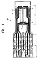
- FIG 4 is a plan view of the FPC cable 60.
- the FPC cable 60 is largely divided into a pad area A having a plurality of contact pads (indicated by alphabets), which contact the contact terminals (not shown) provided in the head transfer mechanism of a printer, and a bonding area B where the conductors 61 bonded to the pads 20 of the substrate 10 of an inkjet print head are arranged.
- Reference numeral 11 denotes a nozzle area formed on the substrate 10.
- the bonding portions (front ends) of the conductors 61 are arranged in areas C corresponding to the short edges of the substrate 10.
- the first embodiment shown in Figure 3 is characterized in that the bonding portions of conductors 61 are bonded to opposite pads 20 installed on opposite edges of the substrate 10.
- two conductors 61 are bonded to two opposite pads 20 installed on both ends of the substrate 10 at a time. Bonding energy is created by heat or pressure.
- the FPC cable 60 is arranged on the substrate 10 mounted on the stage 50, such that it is placed at a bonding location as shown in Figure 4.
- the bonding tool 40 heated to a predetermined temperature performs hot pressure welding by depressing the conductors 61 down on the pads 20 on the substrate 10 placed directly under the conductors 61. At this time, heat also comes out of the stage 50, and the substrate 10 and the pads 20 may be heated.
- reference numeral 42 denotes a recess formed to protect elements such as heaters formed on a substrate.
- the conductors 61 are bonded to opposite pads installed on opposite ends of the substrate 10.
- two adjacent pads 20 installed on one edge of a substrate may be bonded to corresponding conductors 61 by a bonding tool 40a designed for this style of bonding.
- the method of Figure 6 corresponds to a second embodiment of the present invention.
- the bonding tools 40 and 40a are movable over the surface of the stage 50 as in general bonding apparatuses, so that the other pads installed on the substrate can also be bonded.
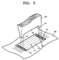
- a bonding method according to preferred embodiments of the present invention is characterized in that at least two pads are bonded to corresponding conductors at a time and that any at least two pads can be selected. However, it is preferable that opposite pads on both ends of the substrate 10 are selected and bonded, as shown in Figures 3 and 5.
- a conductive bump 70 between the pad 20 and the conductor 61 is installed between the pad 20 and the conductor 61, as shown in Figure 7.
- the method of Figure 7 corresponds to a third embodiment of the present invention.
- the bump 70 is made of lead, gold, or other conductive materials. The type of material of such a bump does not restrict the technical scope of the present invention.
- the bump 70 installed on the pad 20 is formed by a general method, so the formation method will not be described.
- a bonding tool 40b has a size that covers all of the pads 20 on the substrate 10, and two opposite tips 41b are formed on the bottom of the bonding tool 40b in dam shapes extending along both ends of a substrate. That is, the dam-shaped tips 41b bond all of the pads arranged on opposite edges of the substrate10 to corresponding conductors 61 using heat and pressure.
- an FPC cable 60a includes upper and lower protect films 62a and 62b formed on the upper and lower sides of a conductor 61, respectively.
- the FPC cable 60a has the upper protect film 62a that completely covers the conductor 61.
- the FPC cable 60 can be applied to the fifth embodiment of Figure 9.
- the bonding apparatus of Figure 9 is characterized in that a tip 41c of a bonding tool 40c has a protrusion 41d extending to the outside of the substrate 10. Since the protrusion 41d protrudes lower than the tip 41c, the FPC cable 60a is bended beside the substrate 10 upon bonding. Since the bending is permanent, even after the bonding is completed, the bended portion of the FPC cable 60a lasts permanently in a shape as shown in Figure 10. In this way, the bonding for electrically connecting the FPC cable 60a to the substrate 10 is completed. As shown in Figure 10, exposed portions of the conductor 61 and pad 20 are encapsulated by resin, forming an encapsulator 80.
- the FPC cable 60a bended at both ends of the substrate 10 When the FPC cable 60a bended at both ends of the substrate 10 is installed on a cartridge 90 for an ink jet printer, as shown in Figure 11, it is closely attached to the upper surface of the cartridge 90. However, if the FPC cable 60a is not bent at both ends of the substrate 10, it is combined with a cartridge in a state of being positioned relatively high beside the substrate 10. This may cause a difficulty in wiping a nozzle area.
- reference numeral 91 denotes resin, such as epoxy, for attaching the substrate 10 to an ink reservoir and preventing ink leakage
- reference numeral 92 denotes a double-sticky tape for attaching the cable 60a to the cartridge 90. Since the upper surface of the conductor 61 is covered by the protect film 62a, 62b, the encapsulator 80 is formed of a small amount of resin supplied to only the exposed portions of the conductor 61 and the pad 20. Consequently, the encapsulator 80 is small and especially is not high from the substrate. Hence, the interval between the substrate 10 and a medium, such as paper, depending on an encapsulator can be significantly narrowed. In the prior art, since the upper surface of a conductor is exposed, much resin enough to cover the exposed portion must be supplied, so that a high encapsulator is created. This leads to a large interval between a medium to be printed on and the surface of the substrate 10.
- the FPC cable 60a capable of creating a low encapsulator can be applied to the previous embodiments.
- Figure 12 shows the structure of an FPC cable 60b capable of being applied to the previous embodiments.
- the bonding portion of the conductor 61 is covered by upper and lower protect films 62a and 62b, having an aperture 62c formed in the portion facing the pad 20.
- the FPC cable 60b is electrically connected to the substrate 10 via the aperture 62c by bonding the conductor 61 to the pad 20.
- the bump 70 is installed in the aperture 62c in order to help more effective bonding between the pad 20 and the conductor 61.
- an electrical defect due to pad peel-off phenomenon which is created by an conventional tape automated bonding (TAB) method in which the conductors of an FPC cable are bonded to the pads on a substrate in a manner where one conductor is bonded to a pad at a time, is removed to increase the reliability of bonding.
- the reliability is maximized by bonding at least two pads at a time, more preferably, by bonding all of the pads on a substrate at a time, which is called gang bonding.
- the interval between the substrate and a medium is narrowed, reducing the interlaced distance of droplet discharged from the substrate. Thus, more stable printing quality with higher density is provided.
Landscapes
- Engineering & Computer Science (AREA)
- Manufacturing & Machinery (AREA)
- Microelectronics & Electronic Packaging (AREA)
- Particle Formation And Scattering Control In Inkjet Printers (AREA)
- Accessory Devices And Overall Control Thereof (AREA)
- Combinations Of Printed Boards (AREA)
Abstract
Description
- The present invention relates to ink jet print heads, methods of bonding a flexible printed circuit (FPC) cable for an ink jet print head, and to apparatus adopting the method.
- In an ink jet head adopting an electro-thermal transducing technique for discharging ink droplet using bubbles obtained by instantaneously heating ink, a substrate having heaters and nozzles thereon is included. The substrate also includes a plurality of signal lines electrically connected to the heaters, and a plurality of electric pads arranged on the edge of the substrate in an inline configuration in order to achieve the contact of the signal lines and an external circuit.
- The pads are connected to an FPC cable on which a plurality of conductors corresponding to the pads are arranged side by side. The pads are bonded to the conductors by thermosonic bonding.
- U.S. Patent Nos. US-A-4,635,073 and US-A-6,126,271 disclose a method of bonding pads to conductors using a thermosonic bonding technique. The thermosonic bonding technique corresponds to a single point bonding method of bonding a single point at a time. Accordingly, as shown in Figure 1, in a state where a
conductor 3 contacts apad 2 installed on asubstrate 1 and then athermosonic bonding tool 4 contacts the resultant substrate structure, thepad 2 is bonded to theconductor 3 by one time bonding. In this way, the other pads and conductors are sequentially bonded together. According to this conventional method, as many bonding processes as the number of pads installed on a substrate must be performed, consequently requiring a lot of time to bond an FPC cable to a single substrate. - In addition, the bonding tool partially contacts the conductor upon thermosonic bonding, and hence the contacted portion of the conductor on which vibration energy generated by ultrasonic is focused may be deformed. Accordingly, the rigidity of the contacted portion decreases, so that the conductor may be easily separated from the pad.
- It is an aim of preferred embodiments of the present invention to provide an ink jet print head, a method of bonding a flexible printed circuit (FPC) cable for an ink jet print head, and an apparatus adopting the method, in which a reduction in the time for bonding conductors leads to a decrease in the time required for manufacturing an ink jet print head.
- Another aim of preferred embodiments of the present invention is to provide an ink jet print head, a method of bonding an FPC cable for an ink jet print head, and an apparatus adopting the method, in which the portion where an FPC conductor and a pad are joined together provides an increased structural intensity.
- Still another aim of preferred embodiments of the present invention is to provide an ink jet print head, a method of bonding an FPC cable for an ink jet print head, and an apparatus adopting the method, in which the printing quality is increased by a reduction in the interlaced distance of droplet.
- The present invention provides, in a first aspect, a method of bonding an FPC for an ink jet print head, the method comprising: preparing a substrate for an ink jet print head, the substrate having a plurality of resistive heaters, a plurality of signal lines connected to the resistive heaters, and a plurality of electrical pads for connecting the signal lines to the outside; preparing an FPC cable having a plurality of conductors having bonding portions, the conductors corresponding to the pads; preparing a bonding apparatus adopting a hot pressure welding technique, the bonding apparatus having a stage for mounting the substrate on and a bonding tool for pressing the bonding portions of the conductors down on the pads of the substrate and heating the bonding portions attached to the pads; mounting the substrate on the stage of the bonding apparatus in order to combine the substrate with the FPC cable; arranging the FPC cable on the substrate so that the bonding portions of the conductors face the corresponding pads; and pressing at least two conductors down on the corresponding pads at a time using the bonding tool and heating the conductors using the bonding tool, to thereby bond the conductors to the pads.
- The present invention provides, in a second aspect, another method of bonding an FPC for an ink jet print head, the method comprising: preparing a substrate for an ink jet print head, the substrate having a plurality of resistive heaters, a plurality of signal lines connected to the resistive heaters, and a plurality of electrical pads for connecting the signal lines to the outside; preparing an FPC cable, the FPC cable having a plurality of conductors having bonding portions facing the pads, an upper protect film completely covering the upper surface of a conductor, and a lower protect film covering the lower surface of the conductor except for the bonding portion facing a pad; preparing a bonding apparatus adopting a hot pressure welding technique, the bonding apparatus having a stage for mounting the substrate on and a bonding tool for pressing the bonding portions of the conductors down on the pads of the substrate and heating the bonding portions attached to the pads; mounting the substrate on the stage of the bonding apparatus in order to combine the substrate with the FPC cable; arranging the FPC cable on the substrate so that the bonding portions of the conductors face the corresponding pads; and pressing at least two conductors down on the corresponding pads at a time using the bonding tool and heating the conductors using the bonding tool, to thereby bond the conductors to the pads.
- According to an embodiment of the present invention, in the above methods, a tip for bringing the bonding portion of a conductor in contact with a corresponding pad is formed at both edges of the bonding tool.
- Preferably, when the bonding tool bonds the conductors to the pads, the pads installed on one edge of the substrate are bonded symmetrically to the pads installed on the other edge of the substrate. Also, it is preferable that all of the pads on the substrate are bonded to the corresponding conductors at a time. Preferably, when the bonding tool bonds the conductors to the pads, it bends the FPC cable so that the bent portion of the FPC cable is placed at the rear of the substrate.
- According to a preferred embodiment of the bonding method, bonding is performed with a bump interposed between the bonding portion of a conductor and a pad. Preferably, the lower protect film has an aperture facing a pad, and a bump is inserted into the aperture and electrically connects the bonding portion of a conductor to a corresponding pad.
- The present invention, in a third aspect, provides a bonding apparatus for bonding the bonding portions of an FPC cable to the pads of a substrate in order to electrically connect the substrate for an ink jet print head, the substrate having a plurality of resistive heaters, a plurality of signal lines connected to the resistive heaters, and a plurality of electrical pads for connecting the signal lines to the outside, to the FPC cable having a plurality of conductors having bonding portions facing the pads, the bonding apparatus comprising a stage on which the substrate is mounted with the pads facing upward, and a bonding tool that moves up and down over the stage and has a bonding tip for pressing at least two bonding portions down on the corresponding pads and heating the bonding portions in contact with the pads to thereby bond the bonding portion to the pads using a hot pressure welding technique.
- In the bonding apparatus, preferably, the bonding tool has a tip for bringing the bonding portions of the conductors of the FPC cable in contact with corresponding pads. More preferably, the tip protrudes from both edges of the bonding tool in order to bond opposite conductors to corresponding opposite pads among the pads formed on both edges of the substrate.
- According to a preferred embodiment of the present invention for the above bonding apparatus, the bonding tool has a dam-shaped tip that covers all of the pads formed on the substrate. Also, the dam-shaped tip is symmetrically formed at both ends of the bonding tool such that the dam-shaped tip covers all of the pads formed along both edges of the substrate. Furthermore, the bonding tool has a protruding extension for bending the FPC cable beside the each edge of the substrate so that the FPC cable is placed from the upper surface level of the substrate to the position at the rear of the substrate.
- The present invention, in a fourth aspect, provides an ink jet print head comprising a substrate having a plurality of resistive heaters, a plurality of signal lines connected to the resistive heaters, and a plurality of electrical pads for connecting the signal lines to an external circuit; and an FPC cable having a plurality of conductors and upper and lower films for protecting a conductor, wherein each of the conductors has a bonding portion to be bonded to a corresponding pad, wherein the conductors of the FPC cable are bonded to the corresponding pads of the substrate by hot pressure welding, and the bonding portion of a conductor that faces a corresponding pad is covered by the upper and lower films.
- In the above-described ink jet print head, preferably, the FPC cable is bent such that its bent portion is placed at the rear of the substrate. It is also preferable that the upper and lower surfaces of a conductor is covered by the upper and lower films, and the lower film has a window formed directly over a corresponding pad to allow the conductor to contact the pad.
- According to a preferred embodiment of the present invention for the ink jet print head, a conductive bump is interposed between the bonding portion of a conductor and a corresponding pad.
- The present invention will become more apparent by describing in detail preferred embodiments thereof, by way of example only, with reference to the attached drawings; in which:
- Figure 1 is a schematic diagram for illustrating a method of bonding a flexible printed circuit (FPC) cable for an ink jet print head using a conventional thermosonic welding technique;
- Figure 2 is a flowchart for illustrating a method of bonding an FPC cable for an ink jet print head, according to the present invention;
- Figure 3 is a schematic structure diagram of a bonding apparatus according to the present invention for explaining a method of bonding an FPC cable for an ink jet print head according to a first embodiment of the present invention;
- Figure 4 is a plan view of an FPC cable used for an ink jet print head;
- Figure 5 is a perspective view showing a bonding manner in which two pads at one time are bonded to an FPC cable by the FPC cable bonding method of Figure 3;
- Figure 6 is a perspective view showing a method of bonding an FPC cable for an ink jet print head according to a second embodiment of the present invention;
- Figure 7 is a schematic diagram for illustrating a method of bonding an FPC cable for an ink jet print head according to a third embodiment of the present invention;
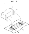
- Figure 8 is a perspective view of a bonding tool of a bonding apparatus according to the present invention for explaining a method of bonding an FPC cable for an ink jet print head according to a fourth embodiment of the present invention;
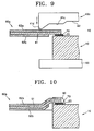
- Figure 9 is a cross-sectional diagram for illustrating a method of bonding an FPC cable for an ink jet print head according to a fifth embodiment of the present invention;
- Figure 10 is a partial cross-section of a substrate to which an FPC cable is bonded by the method of Figure 9;
- Figure 11 is a partial cross-section of an ink jet print head cartridge on which the substrate to which an FPC cable is bonded by the method of Figure 9 is installed; and
- Figure 12 is a cross-sectional view for illustrating a method of bonding an FPC cable for an ink jet print head according to a sixth embodiment of the present invention.
-
- Hereinafter, an ink jet print head is not described but will be understood through the description of bonding methods and apparatuses according to the present invention.
- Preferred embodiments of the present invention basically adopt hot pressure welding instead of thermosonic bonding, that is, thermosonic welding using local kinetic energy. In hot pressure welding, a fragile substrate is not subject to vibration impact, so that simultaneous bonding with respect to several pads is possible in contrast with thermosonic bonding.
- Figure 2 is a flowchart for illustrating a bonding method according to an embodiment of the present invention. Referring to Figure 2, first of all, a substrate for an ink jet print head is prepared, in
step 91. Then, a flexible printed circuit (FPC) cable to be bonded to the substrate is prepared, instep 92. Next, a bonding apparatus for bonding the conductors of the FPC cable to the pads on the substrate using the hot pressure welding technique is prepared, instep 93. Thereafter, the substrate is mounted on the stage of the bonding apparatus, instep 94. Subsequently, the FPC cable is arranged on the substrate, instep 95. Next, the bonding tool of the bonding apparatus bonds the conductors of the FPC cable to the pads on the substrate using the hot pressure welding technique, instep 96. At this time, at least two conductors are bonded to at least two pads. This bonding repeats until all of the pads on the substrate are bonded to the corresponding conductors, instep 97. However, all of the pads can be simultaneously bonded to the corresponding conductors at a time. - Figure 3 is a schematic structure diagram of a bonding apparatus according to an embodiment of the present invention in which a bonding tool bonds an FPC cable to a substrate in a bonding method according to a first embodiment of the present invention. Referring to Figure 3, a
substrate 10 to be bonded is mounted on astage 50 of a bonding apparatus adopting a hot pressure welding technique. Thesubstrate 10 includes a plurality of resistive heaters, a plurality of signal lines connected to the heaters, and a plurality of electric pads for connecting the signal lines to an external circuit. Figure 3 shows only theelectric pads 20. - The
conductors 61 of aFPC cable 60 are placed on thepads 20 and depressed by thetip 41 of abonding tool 40. Theconductors 61 of theFPC cable 60 are protected by upper and lower insulative protectfilms 62. - Figure 4 is a plan view of the
FPC cable 60. TheFPC cable 60 is largely divided into a pad area A having a plurality of contact pads (indicated by alphabets), which contact the contact terminals (not shown) provided in the head transfer mechanism of a printer, and a bonding area B where theconductors 61 bonded to thepads 20 of thesubstrate 10 of an inkjet print head are arranged.Reference numeral 11 denotes a nozzle area formed on thesubstrate 10. In theFPC cable 60 of Figure 3, the bonding portions (front ends) of theconductors 61 are arranged in areas C corresponding to the short edges of thesubstrate 10. - Referring back to Figure 3, the first embodiment shown in Figure 3 is characterized in that the bonding portions of
conductors 61 are bonded toopposite pads 20 installed on opposite edges of thesubstrate 10. In this embodiment, twoconductors 61 are bonded to twoopposite pads 20 installed on both ends of thesubstrate 10 at a time. Bonding energy is created by heat or pressure. TheFPC cable 60 is arranged on thesubstrate 10 mounted on thestage 50, such that it is placed at a bonding location as shown in Figure 4. Next, thebonding tool 40 heated to a predetermined temperature performs hot pressure welding by depressing theconductors 61 down on thepads 20 on thesubstrate 10 placed directly under theconductors 61. At this time, heat also comes out of thestage 50, and thesubstrate 10 and thepads 20 may be heated. This hot pressure wielding is achieved within a very short period of time, in which the bottoms of the bonding portions of theconductors 61 and the pads are locally melted and joined together. In Figure 3,reference numeral 42 denotes a recess formed to protect elements such as heaters formed on a substrate. - In the first embodiment as shown in Figure 3, the
conductors 61 are bonded to opposite pads installed on opposite ends of thesubstrate 10. However, as shown in Figure 6, twoadjacent pads 20 installed on one edge of a substrate may be bonded to correspondingconductors 61 by abonding tool 40a designed for this style of bonding. The method of Figure 6 corresponds to a second embodiment of the present invention. Thebonding tools stage 50 as in general bonding apparatuses, so that the other pads installed on the substrate can also be bonded. A bonding method according to preferred embodiments of the present invention is characterized in that at least two pads are bonded to corresponding conductors at a time and that any at least two pads can be selected. However, it is preferable that opposite pads on both ends of thesubstrate 10 are selected and bonded, as shown in Figures 3 and 5. - In order to achieve more effective bonding, it is preferable to install a
conductive bump 70 between thepad 20 and theconductor 61, as shown in Figure 7. The method of Figure 7 corresponds to a third embodiment of the present invention. Thebump 70 is made of lead, gold, or other conductive materials. The type of material of such a bump does not restrict the technical scope of the present invention. Thebump 70 installed on thepad 20 is formed by a general method, so the formation method will not be described. - In a fourth embodiment of the present invention as shown in Figure 8, all of the
pads 20 on thesubstrate 10 are bonded to correspondingconductors 61 at a time. That is, this bonding corresponds to gang bonding. To do this, abonding tool 40b has a size that covers all of thepads 20 on thesubstrate 10, and twoopposite tips 41b are formed on the bottom of thebonding tool 40b in dam shapes extending along both ends of a substrate. That is, the dam-shapedtips 41b bond all of the pads arranged on opposite edges of the substrate10 to correspondingconductors 61 using heat and pressure. - In a bonding method according to preferred embodiments of the present invention, not only the bonding style but also the shape of an FPC cable is properly changed, as shown in Figure 9. Referring to Figure 9, the
substrate 10 is mounted on thestage 50. A pad is installed on the edge of thesubstrate 10, and thebump 70 is then installed on thepad 20. AnFPC cable 60a includes upper and lower protectfilms conductor 61, respectively. In a fifth embodiment of the present invention as shown in Figure 9, theFPC cable 60a has the upperprotect film 62a that completely covers theconductor 61. However, theFPC cable 60 can be applied to the fifth embodiment of Figure 9. - The bonding apparatus of Figure 9 is characterized in that a
tip 41c of abonding tool 40c has aprotrusion 41d extending to the outside of thesubstrate 10. Since theprotrusion 41d protrudes lower than thetip 41c, theFPC cable 60a is bended beside thesubstrate 10 upon bonding. Since the bending is permanent, even after the bonding is completed, the bended portion of theFPC cable 60a lasts permanently in a shape as shown in Figure 10. In this way, the bonding for electrically connecting theFPC cable 60a to thesubstrate 10 is completed. As shown in Figure 10, exposed portions of theconductor 61 andpad 20 are encapsulated by resin, forming anencapsulator 80. - When the
FPC cable 60a bended at both ends of thesubstrate 10 is installed on acartridge 90 for an ink jet printer, as shown in Figure 11, it is closely attached to the upper surface of thecartridge 90. However, if theFPC cable 60a is not bent at both ends of thesubstrate 10, it is combined with a cartridge in a state of being positioned relatively high beside thesubstrate 10. This may cause a difficulty in wiping a nozzle area. - In Figure 11,
reference numeral 91 denotes resin, such as epoxy, for attaching thesubstrate 10 to an ink reservoir and preventing ink leakage, andreference numeral 92 denotes a double-sticky tape for attaching thecable 60a to thecartridge 90. Since the upper surface of theconductor 61 is covered by theprotect film encapsulator 80 is formed of a small amount of resin supplied to only the exposed portions of theconductor 61 and thepad 20. Consequently, theencapsulator 80 is small and especially is not high from the substrate. Hence, the interval between thesubstrate 10 and a medium, such as paper, depending on an encapsulator can be significantly narrowed. In the prior art, since the upper surface of a conductor is exposed, much resin enough to cover the exposed portion must be supplied, so that a high encapsulator is created. This leads to a large interval between a medium to be printed on and the surface of thesubstrate 10. - The
FPC cable 60a capable of creating a low encapsulator can be applied to the previous embodiments. - Figure 12 shows the structure of an
FPC cable 60b capable of being applied to the previous embodiments. In theFPC cable 60b, which is a transformation of theFPC cable 60a shown in Figures 9 through 11, the bonding portion of theconductor 61 is covered by upper and lower protectfilms aperture 62c formed in the portion facing thepad 20. TheFPC cable 60b is electrically connected to thesubstrate 10 via theaperture 62c by bonding theconductor 61 to thepad 20. In a sixth embodiment of the present invention, as shown in Figure 12, thebump 70 is installed in theaperture 62c in order to help more effective bonding between thepad 20 and theconductor 61. - In the above-described preferred embodiments of the present invention, an electrical defect due to pad peel-off phenomenon, which is created by an conventional tape automated bonding (TAB) method in which the conductors of an FPC cable are bonded to the pads on a substrate in a manner where one conductor is bonded to a pad at a time, is removed to increase the reliability of bonding. The reliability is maximized by bonding at least two pads at a time, more preferably, by bonding all of the pads on a substrate at a time, which is called gang bonding. Also, the interval between the substrate and a medium is narrowed, reducing the interlaced distance of droplet discharged from the substrate. Thus, more stable printing quality with higher density is provided.
- While this invention has been particularly shown and described with reference to preferred embodiments thereof, it will be understood by those skilled in the art that various changes in form and details may be made therein without departing from the spirit and scope of the invention as defined by the appended claims.
- The reader's attention is directed to all papers and documents which are filed concurrently with or previous to this specification in connection with this application and which are open to public inspection with this specification, and the contents of all such papers and documents are incorporated herein by reference.
- All of the features disclosed in this specification (including any accompanying claims, abstract and drawings), and/or all of the steps of any method or process so disclosed, may be combined in any combination, except combinations where at least some of such features and/or steps are mutually exclusive.
- Each feature disclosed in this specification (including any accompanying claims, abstract and drawings), may be replaced by alternative features serving the same, equivalent or similar purpose, unless expressly stated otherwise. Thus, unless expressly stated otherwise, each feature disclosed is one example only of a generic series of equivalent or similar features.
- The invention is not restricted to the details of the foregoing embodiment(s). The invention extends to any novel one, or any novel combination, of the features disclosed in this specification (including any accompanying claims, abstract and drawings), or to any novel one, or any novel combination, of the steps of any method or process so disclosed.
Claims (24)
- A method of bonding a flexible printed circuit (FPC) for an ink jet print head, the method comprising:preparing (91) a substrate (10) for an ink jet print head, the substrate (10) having a plurality of resistive heaters, a plurality of signal lines connected to the resistive heaters, and a plurality of electrical pads (20) for connecting the signal lines to the outside;preparing (92) an FPC cable (60) having a plurality of conductors (61) having bonding portions, the conductors corresponding to the pads (20);preparing (93) a bonding apparatus (40, 50) adopting a hot pressure welding technique, the bonding apparatus having a stage (50) for mounting the substrate (10) on and a bonding tool (40) for pressing the bonding portions of the conductors down on the pads (20) of the substrate and heating the bonding portions attached to the pads (20);mounting (94) the substrate (10) on the stage (50) of the bonding apparatus (40, 50) in order to combine the substrate (10) with the FPC cable (60);arranging (95) the FPC cable (60) on the substrate (10) so that the bonding portions of the conductors (61) face the corresponding pads (20); andpressing (96) at least two conductors (61) down on the corresponding pads (20) at a time using the bonding tool (40, 50) and heating the conductors (61) using the bonding tool (40, 50), to thereby bond the conductors (61) to the pads (20).
- The method of claim 1, wherein a tip (41) for bringing the bonding portion of a conductor in contact with a corresponding pad is formed at both edges of the bonding tool.
- The method of claim 2, wherein, when the bonding tool (40) bonds the conductors (61) to the pads (20), the pads (20) installed on one edge of the substrate (10) are bonded symmetrically to the pads (20) installed on the other edge of the substrate (10).
- The method of any preceding claim, wherein all of the pads (20) on the substrate (10) are bonded to the corresponding conductors (61) at a time.
- The method of any preceding claim, wherein, when the bonding tool (40, 50) bonds the conductors (61) to the pads (20), it bends the FPC cable (60) so that the bent portion of the FPC cable (60) is placed at the rear of the substrate (10).
- The method of any one of claims 1 through 4, wherein bonding is performed with a bump (70) interposed between the bonding portion (40) of a conductor and a corresponding pad (20).
- A method of bonding a flexible printed circuit (FPC) for an ink jet print head, the method comprising:preparing (91) a substrate (10) for an ink jet print head, the substrate (10) having a plurality of resistive heaters, a plurality of signal lines connected to the resistive heaters, and a plurality of electrical pads (20) for connecting the signal lines to the outside;preparing (92) an FPC cable (60), the FPC cable having a plurality of conductors (61) having bonding portions facing the pads (20), an upper protect film (62a) completely covering the upper surface of a conductor (61), and a lower protect film (62b) covering the lower surface of the conductor (61) except for the bonding portion facing a pad (20);preparing (93) a bonding apparatus (40, 50) adopting a hot pressure welding technique, the bonding apparatus (40, 50) having a stage (50) for mounting the substrate on and a bonding tool (40) for pressing the bonding portions of the conductors (61) down on the pads (20) of the substrate (10) and heating the bonding portions attached to the pads (20) ;mounting (94) the substrate (10) on the stage (50) of the bonding apparatus (40, 50) in order to combine the substrate (10) with the FPC cable (60);arranging (95) the FPC cable (60) on the substrate (10) so that the bonding portions of the conductors (61) face the corresponding pads (20); andpressing (96) at least two conductors (61) down on the corresponding pads (20) at a time using the bonding tool (40, 50) and heating the conductors (61) using the bonding tool (40, 50), to thereby bond the conductors (61) to the pads (20).
- The method of claim 7, wherein a tip (41) for bringing the bonding portion of a conductor (61) in contact with a corresponding pad (20) is formed at both edges of the bonding tool (40, 50).
- The method of claim 8, wherein, when the bonding tool (40, 50) bonds the conductors (61) to the pads (20), the pads (20) installed on one edge of the substrate (10) are bonded symmetrically to the pads (20) installed on the other edge of the substrate (10).
- The method of any one of claims 7-9, wherein all of the pads (20) on the substrate (10) are bonded to the corresponding conductors (61) at a time.
- The method of any one of claims 7 through 10, wherein, when the bonding tool (40, 50) bonds the conductors (61) to the pads (20), it bends the FPC cable (60) beside the edges of the substrate (10) so that the bent portion of the FPC cable (60) is placed at the rear of the substrate (10).
- The method of any one of claims 7 through 10, wherein bonding is performed with a bump (70) interposed between the bonding portion of a conductor (61) and a pad (20).
- The method of any one of claims 7 through 10, wherein the lower protect film (62b) has an aperture facing a pad (20).
- The method of claim 13, wherein a bump (70) is inserted into the aperture and electrically connects the bonding portion of a conductor (61) to a corresponding pad (20).
- A bonding apparatus (40, 50) for bonding the bonding portions of an FPC cable (60) to the pads (20) of a substrate (10) in order to electrically connect the substrate (10) for an ink jet print head, the substrate (10) having a plurality of resistive heaters, a plurality of signal lines connected to the resistive heaters, and a plurality of electrical pads (20) for connecting the signal lines to the outside, to the FPC cable (60) having a plurality of conductors (61) having bonding portions facing the pads (20), the bonding apparatus (40, 50) comprising:a stage (50) on which the substrate (10) is mounted with the pads (20) facing upward; anda bonding tool (40) that moves up and down over the stage (50) and has a bonding tip (41) for pressing at least two bonding portions down on the corresponding pads (20) and heating the bonding portions in contact with the pads (30) to thereby bond the bonding portion to the pads (20) using a hot pressure welding technique.
- The bonding apparatus (40, 50) of claim 15, wherein the bonding tool (40) has a tip (41) for bringing the bonding portions of the conductors (61) of the FPC cable (60) in contact with corresponding pads (20).
- The bonding apparatus (40, 50) of claim 16, wherein the tip (41) protrudes from both edges of the bonding tool (40) in order to bond opposite conductors (61) to corresponding opposite pads (20) among the pads (20) formed on both edges of the substrate (10).
- The bonding apparatus (40, 50) of any one of claims 15-17, wherein the bonding tool (40) has a dam-shaped tip (41b) that covers all of the pads (20) formed on the substrate (10).
- The bonding apparatus (40, 50) of claim 18, wherein the dam-shaped tip (41b) is symmetrically formed at both ends of the bonding tool (40) such that the dam-shaped tip (41b) covers all of the pads (20) formed along both edges of the substrate (10).
- The bonding apparatus (40, 50) of any one of claims 15 through 19, wherein the bonding tool (40) has a protruding extension for bending the FPC cable (66) beside the each edge of the substrate (10) so that the FPC cable (60) is placed from the upper surface level of the substrate (10) to the position at the rear of the substrate.
- An ink jet print head comprising:a substrate (10) having a plurality of resistive heaters, a plurality of signal lines connected to the resistive heaters, and a plurality of electrical pads (20) for connecting the signal lines to an external circuit; andan FPC cable (60) having a plurality of conductors (61) and upper (62a) and lower (62b) films for protecting a conductor (61), wherein each of the conductors (61) has a bonding portion to be bonded to a corresponding pad (20), wherein the conductors (61) of the FPC cable (10) are bonded to the corresponding pads (20) of the substrate (10) by hot pressure welding, and the bonding portion of a conductor (61) that faces a corresponding pad (20) is covered by the upper and lower films (62a, 62b).
- The ink jet print head of claim 21, wherein the FPC cable (60) is bent such that its bent portion is placed at the rear of the substrate (10).
- The ink jet print head of claim 21 or 22, wherein the upper and lower surfaces of a conductor (61) is covered by the upper and lower films (62a, 62b), and the lower film (62b) has a window formed directly over a corresponding pad (20) to allow the conductor (61) to contact the pad (20).
- The ink jet print head of any one of claims 21-23, wherein a conductive bump (70) is interposed between the bonding portion of a conductor (61) and a corresponding pad (20).
Applications Claiming Priority (2)
| Application Number | Priority Date | Filing Date | Title |
|---|---|---|---|
| KR2002027867 | 2002-05-20 | ||
| KR10-2002-0027867A KR100462604B1 (en) | 2002-05-20 | 2002-05-20 | Ink jet print head, bonding method of flexible printed circuit cable for ink jet print head and the apparatus adopting the same |
Publications (2)
| Publication Number | Publication Date |
|---|---|
| EP1364788A2 true EP1364788A2 (en) | 2003-11-26 |
| EP1364788A3 EP1364788A3 (en) | 2004-05-06 |
Family
ID=29398531
Family Applications (1)
| Application Number | Title | Priority Date | Filing Date |
|---|---|---|---|
| EP02257528A Withdrawn EP1364788A3 (en) | 2002-05-20 | 2002-10-30 | Ink jet print head and method and apparatus for bonding flexible printed circuit cable for ink jet print head |
Country Status (5)
| Country | Link |
|---|---|
| US (1) | US6902261B2 (en) |
| EP (1) | EP1364788A3 (en) |
| JP (1) | JP2003334960A (en) |
| KR (1) | KR100462604B1 (en) |
| CN (1) | CN1459352A (en) |
Families Citing this family (14)
| Publication number | Priority date | Publication date | Assignee | Title |
|---|---|---|---|---|
| US7754604B2 (en) * | 2003-08-26 | 2010-07-13 | Novellus Systems, Inc. | Reducing silicon attack and improving resistivity of tungsten nitride film |
| JP2006068989A (en) * | 2004-09-01 | 2006-03-16 | Seiko Epson Corp | Droplet discharge head, droplet discharge device, and method of manufacturing droplet discharge head |
| CN100384629C (en) * | 2004-11-29 | 2008-04-30 | 晶强电子股份有限公司 | Flexible circuit board of ink-jet printing head and its manufacturing method |
| JP4779636B2 (en) * | 2005-12-20 | 2011-09-28 | セイコーエプソン株式会社 | Droplet discharge head and droplet discharge apparatus |
| US7835158B2 (en) * | 2005-12-30 | 2010-11-16 | Micron Technology, Inc. | Connection verification technique |
| CN101939170B (en) * | 2007-12-07 | 2012-08-29 | 惠普开发有限公司 | Print cartridge |
| US7896470B2 (en) * | 2007-12-07 | 2011-03-01 | Hewlett-Packard Development Company, L.P. | Print cartridge |
| WO2014051541A1 (en) * | 2012-09-25 | 2014-04-03 | Hewlett-Packard Development Company, L.P. | Print head die |
| WO2014051543A1 (en) | 2012-09-25 | 2014-04-03 | Hewlett-Packard Development Company, L.P. | Print head die |
| JP6290814B2 (en) * | 2015-03-30 | 2018-03-07 | 株式会社東芝 | Inkjet head, inkjet head manufacturing method, and inkjet recording apparatus |
| JP7053786B2 (en) * | 2017-07-26 | 2022-04-12 | ヒューレット-パッカード デベロップメント カンパニー エル.ピー. | Die contact formation |
| CN107984902B (en) * | 2017-11-06 | 2019-03-15 | 浙江省东阳市东磁诚基电子有限公司 | Band FPC vibrating motor spray code spraying apparatus and technique |
| CN111787692A (en) * | 2019-04-03 | 2020-10-16 | 研能科技股份有限公司 | Inkjet chip package structure |
| CN113496968A (en) * | 2021-07-07 | 2021-10-12 | 南昌黑鲨科技有限公司 | Heat dissipation assembly for heat dissipation of chip and preparation process method |
Citations (2)
| Publication number | Priority date | Publication date | Assignee | Title |
|---|---|---|---|---|
| US4635073A (en) | 1985-11-22 | 1987-01-06 | Hewlett Packard Company | Replaceable thermal ink jet component and thermosonic beam bonding process for fabricating same |
| US6126271A (en) | 1997-02-19 | 2000-10-03 | Canon Kabushiki Kaisha | Method for manufacturing a liquid jet recording head held in place by a vacuum using a single-point bonder with a particular tip construction and a head manufactured by this method |
Family Cites Families (13)
| Publication number | Priority date | Publication date | Assignee | Title |
|---|---|---|---|---|
| EP0032437A1 (en) * | 1980-01-16 | 1981-07-22 | American Coldset Corporation | Thermocompression bonding tool |
| JPH02135797A (en) * | 1988-11-17 | 1990-05-24 | Seiko Epson Corp | Heating tool structure for outer lead bonding and bonder |
| JPH0414231A (en) * | 1990-05-07 | 1992-01-20 | Toshiba Corp | Press mechanism for lead frame and wire bonding device using this |
| JPH0575243A (en) * | 1991-09-18 | 1993-03-26 | Nec Ibaraki Ltd | Lead connection method of integrated circuit rear pressing |
| US5442386A (en) * | 1992-10-13 | 1995-08-15 | Hewlett-Packard Company | Structure and method for preventing ink shorting of conductors connected to printhead |
| JPH06236953A (en) * | 1993-02-10 | 1994-08-23 | Dainippon Printing Co Ltd | Manufacture of lead frame for mounting electronic circuit element and connecting jig for manufacture |
| JP3186925B2 (en) * | 1994-08-04 | 2001-07-11 | シャープ株式会社 | Panel mounting structure, integrated circuit mounting tape and method of manufacturing the same |
| JP3531356B2 (en) * | 1996-05-15 | 2004-05-31 | セイコーエプソン株式会社 | Method of manufacturing inkjet head |
| JPH1058686A (en) | 1996-08-19 | 1998-03-03 | Canon Inc | Ink jet recording head and method of manufacturing the same |
| EP0999060B1 (en) * | 1998-10-27 | 2005-04-20 | Canon Kabushiki Kaisha | Head holder, head assembly, head cartridge, ink jet recorder, and method for manufacturing head assembly |
| CN1273371C (en) * | 1999-03-31 | 2006-09-06 | 精工爱普生株式会社 | Narrow-pitch connector, pitch converter, micromachine, piezoelectric actuator, electrostatic actuator, ink-jet head, ink-jet printer, liquid crystal device, and electronic apparatus |
| JP2001024128A (en) * | 1999-07-06 | 2001-01-26 | Hitachi Cable Ltd | Lead frame manufacturing method |
| US6290331B1 (en) * | 1999-09-09 | 2001-09-18 | Hewlett-Packard Company | High efficiency orifice plate structure and printhead using the same |
-
2002
- 2002-05-20 KR KR10-2002-0027867A patent/KR100462604B1/en not_active Expired - Fee Related
- 2002-10-30 EP EP02257528A patent/EP1364788A3/en not_active Withdrawn
- 2002-10-31 CN CN02147967A patent/CN1459352A/en active Pending
-
2003
- 2003-03-17 US US10/388,422 patent/US6902261B2/en not_active Expired - Fee Related
- 2003-05-09 JP JP2003131510A patent/JP2003334960A/en active Pending
Patent Citations (2)
| Publication number | Priority date | Publication date | Assignee | Title |
|---|---|---|---|---|
| US4635073A (en) | 1985-11-22 | 1987-01-06 | Hewlett Packard Company | Replaceable thermal ink jet component and thermosonic beam bonding process for fabricating same |
| US6126271A (en) | 1997-02-19 | 2000-10-03 | Canon Kabushiki Kaisha | Method for manufacturing a liquid jet recording head held in place by a vacuum using a single-point bonder with a particular tip construction and a head manufactured by this method |
Also Published As
| Publication number | Publication date |
|---|---|
| CN1459352A (en) | 2003-12-03 |
| KR100462604B1 (en) | 2004-12-20 |
| US6902261B2 (en) | 2005-06-07 |
| EP1364788A3 (en) | 2004-05-06 |
| JP2003334960A (en) | 2003-11-25 |
| KR20030089939A (en) | 2003-11-28 |
| US20030214558A1 (en) | 2003-11-20 |
Similar Documents
| Publication | Publication Date | Title |
|---|---|---|
| EP1364788A2 (en) | Ink jet print head and method and apparatus for bonding flexible printed circuit cable for ink jet print head | |
| US6188414B1 (en) | Inkjet printhead with preformed substrate | |
| EP0624472B1 (en) | Ink jet printhead | |
| JPS63265644A (en) | Electrical interconnecting member, interconnecting method, connecting process and electrical interconnecting circuit, and manufacture thereof | |
| US20160001573A1 (en) | Thermal head and thermal printer | |
| EP1080924B1 (en) | Thermal head | |
| CN110356122B (en) | Thermal print head | |
| EP0861725B1 (en) | Ink-jet printhead | |
| US8345437B2 (en) | Connection structure and connection method of wiring board | |
| WO1999065692A1 (en) | A heater chip module for use in an ink jet printer | |
| CN111038111B (en) | Thermal print head and method of manufacturing the same | |
| JP2010260187A (en) | Wiring unit, wiring unit manufacturing method, liquid discharge head, and liquid discharge head manufacturing method | |
| JP3928572B2 (en) | Inkjet head unit | |
| KR100472463B1 (en) | Ink jet print head | |
| EP0366405A2 (en) | Viabond tabcircuit electrical connector | |
| JP2011240512A (en) | Fixing structure of sheet-like member to resin molding, and liquid ejection head using the same | |
| JPH06320721A (en) | Ink jet head | |
| JP2021120231A (en) | Thermal print head | |
| JP3539475B2 (en) | Ink jet recording head and flexible cable connection method | |
| JP5056579B2 (en) | Thermal head manufacturing method, thermal head, and thermal printer | |
| JP2007320229A (en) | Ink jet recording head and method of manufacturing ink jet recording head | |
| JP2022055600A (en) | Thermal print head | |
| JP2003142822A (en) | Connection method of printed wiring board | |
| JP2013145929A (en) | Connection structure and connection method of wiring board | |
| JP2020073344A (en) | Thermal print head |
Legal Events
| Date | Code | Title | Description |
|---|---|---|---|
| PUAI | Public reference made under article 153(3) epc to a published international application that has entered the european phase |
Free format text: ORIGINAL CODE: 0009012 |
|
| 17P | Request for examination filed |
Effective date: 20021114 |
|
| AK | Designated contracting states |
Kind code of ref document: A2 Designated state(s): AT BE BG CH CY CZ DE DK EE ES FI FR GB GR IE IT LI LU MC NL PT SE SK TR |
|
| AX | Request for extension of the european patent |
Extension state: AL LT LV MK RO SI |
|
| PUAL | Search report despatched |
Free format text: ORIGINAL CODE: 0009013 |
|
| AK | Designated contracting states |
Kind code of ref document: A3 Designated state(s): AT BE BG CH CY CZ DE DK EE ES FI FR GB GR IE IT LI LU MC NL PT SE SK TR |
|
| AX | Request for extension of the european patent |
Extension state: AL LT LV MK RO SI |
|
| RIC1 | Information provided on ipc code assigned before grant |
Ipc: 7B 41J 2/16 B Ipc: 7B 41J 2/14 A |
|
| AKX | Designation fees paid |
Designated state(s): DE FR GB |
|
| 17Q | First examination report despatched |
Effective date: 20060626 |
|
| 17Q | First examination report despatched |
Effective date: 20060626 |
|
| STAA | Information on the status of an ep patent application or granted ep patent |
Free format text: STATUS: THE APPLICATION IS DEEMED TO BE WITHDRAWN |
|
| 18D | Application deemed to be withdrawn |
Effective date: 20070823 |