EP1363372A1 - Procédé d'émission d'un photon unique, dispositif semiconducteur et procédé de fabrication correspondants - Google Patents
Procédé d'émission d'un photon unique, dispositif semiconducteur et procédé de fabrication correspondants Download PDFInfo
- Publication number
- EP1363372A1 EP1363372A1 EP03291031A EP03291031A EP1363372A1 EP 1363372 A1 EP1363372 A1 EP 1363372A1 EP 03291031 A EP03291031 A EP 03291031A EP 03291031 A EP03291031 A EP 03291031A EP 1363372 A1 EP1363372 A1 EP 1363372A1
- Authority
- EP
- European Patent Office
- Prior art keywords
- transistor
- integrated circuit
- circuit according
- electron
- grid
- Prior art date
- Legal status (The legal status is an assumption and is not a legal conclusion. Google has not performed a legal analysis and makes no representation as to the accuracy of the status listed.)
- Granted
Links
- 238000000034 method Methods 0.000 title claims abstract description 13
- 238000004519 manufacturing process Methods 0.000 title claims abstract description 11
- 239000004065 semiconductor Substances 0.000 title claims abstract description 10
- 230000008569 process Effects 0.000 title description 3
- XUIMIQQOPSSXEZ-UHFFFAOYSA-N Silicon Chemical compound [Si] XUIMIQQOPSSXEZ-UHFFFAOYSA-N 0.000 claims abstract description 31
- 229910052710 silicon Inorganic materials 0.000 claims abstract description 30
- 239000010703 silicon Substances 0.000 claims abstract description 30
- 239000000758 substrate Substances 0.000 claims abstract description 27
- 230000004044 response Effects 0.000 claims abstract description 8
- 235000001674 Agaricus brunnescens Nutrition 0.000 claims abstract description 5
- 239000002096 quantum dot Substances 0.000 claims description 30
- 239000000463 material Substances 0.000 claims description 14
- GNPVGFCGXDBREM-UHFFFAOYSA-N germanium atom Chemical compound [Ge] GNPVGFCGXDBREM-UHFFFAOYSA-N 0.000 claims description 11
- 229910052732 germanium Inorganic materials 0.000 claims description 9
- 230000003287 optical effect Effects 0.000 claims description 5
- 239000011810 insulating material Substances 0.000 claims description 4
- 230000015572 biosynthetic process Effects 0.000 claims description 3
- 239000011248 coating agent Substances 0.000 claims description 3
- 238000000576 coating method Methods 0.000 claims description 3
- 229910000927 Ge alloy Inorganic materials 0.000 claims description 2
- 229910000676 Si alloy Inorganic materials 0.000 claims description 2
- 230000000149 penetrating effect Effects 0.000 claims 1
- 230000000903 blocking effect Effects 0.000 description 13
- 230000000694 effects Effects 0.000 description 10
- 238000005530 etching Methods 0.000 description 5
- 241000282836 Camelus dromedarius Species 0.000 description 4
- 230000006798 recombination Effects 0.000 description 4
- 238000005215 recombination Methods 0.000 description 4
- 238000006243 chemical reaction Methods 0.000 description 3
- 125000006850 spacer group Chemical group 0.000 description 3
- 229910045601 alloy Inorganic materials 0.000 description 2
- 239000000956 alloy Substances 0.000 description 2
- 230000004888 barrier function Effects 0.000 description 2
- 230000005540 biological transmission Effects 0.000 description 2
- 239000000969 carrier Substances 0.000 description 2
- 238000005229 chemical vapour deposition Methods 0.000 description 2
- 238000005401 electroluminescence Methods 0.000 description 2
- 230000005281 excited state Effects 0.000 description 2
- 238000002513 implantation Methods 0.000 description 2
- 238000002955 isolation Methods 0.000 description 2
- 239000002184 metal Substances 0.000 description 2
- 230000010355 oscillation Effects 0.000 description 2
- 230000000284 resting effect Effects 0.000 description 2
- 238000012552 review Methods 0.000 description 2
- 241000222519 Agaricus bisporus Species 0.000 description 1
- -1 Si 0.75 Ge 0.25 Chemical compound 0.000 description 1
- 229910052581 Si3N4 Inorganic materials 0.000 description 1
- 229910000577 Silicon-germanium Inorganic materials 0.000 description 1
- BOTDANWDWHJENH-UHFFFAOYSA-N Tetraethyl orthosilicate Chemical compound CCO[Si](OCC)(OCC)OCC BOTDANWDWHJENH-UHFFFAOYSA-N 0.000 description 1
- LEVVHYCKPQWKOP-UHFFFAOYSA-N [Si].[Ge] Chemical compound [Si].[Ge] LEVVHYCKPQWKOP-UHFFFAOYSA-N 0.000 description 1
- 230000000981 bystander Effects 0.000 description 1
- 238000004364 calculation method Methods 0.000 description 1
- 230000008878 coupling Effects 0.000 description 1
- 238000010168 coupling process Methods 0.000 description 1
- 238000005859 coupling reaction Methods 0.000 description 1
- 238000000151 deposition Methods 0.000 description 1
- 238000013461 design Methods 0.000 description 1
- 238000009434 installation Methods 0.000 description 1
- 239000012212 insulator Substances 0.000 description 1
- 150000004767 nitrides Chemical class 0.000 description 1
- 238000005457 optimization Methods 0.000 description 1
- 238000000206 photolithography Methods 0.000 description 1
- 239000004038 photonic crystal Substances 0.000 description 1
- 230000010287 polarization Effects 0.000 description 1
- 229910021420 polycrystalline silicon Inorganic materials 0.000 description 1
- 229920005591 polysilicon Polymers 0.000 description 1
- 238000005036 potential barrier Methods 0.000 description 1
- 238000011002 quantification Methods 0.000 description 1
- HQVNEWCFYHHQES-UHFFFAOYSA-N silicon nitride Chemical compound N12[Si]34N5[Si]62N3[Si]51N64 HQVNEWCFYHHQES-UHFFFAOYSA-N 0.000 description 1
- 230000003595 spectral effect Effects 0.000 description 1
- 239000000126 substance Substances 0.000 description 1
- 230000005641 tunneling Effects 0.000 description 1
Images




Classifications
-
- H—ELECTRICITY
- H01—ELECTRIC ELEMENTS
- H01S—DEVICES USING THE PROCESS OF LIGHT AMPLIFICATION BY STIMULATED EMISSION OF RADIATION [LASER] TO AMPLIFY OR GENERATE LIGHT; DEVICES USING STIMULATED EMISSION OF ELECTROMAGNETIC RADIATION IN WAVE RANGES OTHER THAN OPTICAL
- H01S5/00—Semiconductor lasers
- H01S5/30—Structure or shape of the active region; Materials used for the active region
- H01S5/34—Structure or shape of the active region; Materials used for the active region comprising quantum well or superlattice structures, e.g. single quantum well [SQW] lasers, multiple quantum well [MQW] lasers or graded index separate confinement heterostructure [GRINSCH] lasers
- H01S5/341—Structures having reduced dimensionality, e.g. quantum wires
-
- B—PERFORMING OPERATIONS; TRANSPORTING
- B82—NANOTECHNOLOGY
- B82Y—SPECIFIC USES OR APPLICATIONS OF NANOSTRUCTURES; MEASUREMENT OR ANALYSIS OF NANOSTRUCTURES; MANUFACTURE OR TREATMENT OF NANOSTRUCTURES
- B82Y20/00—Nanooptics, e.g. quantum optics or photonic crystals
-
- H—ELECTRICITY
- H01—ELECTRIC ELEMENTS
- H01S—DEVICES USING THE PROCESS OF LIGHT AMPLIFICATION BY STIMULATED EMISSION OF RADIATION [LASER] TO AMPLIFY OR GENERATE LIGHT; DEVICES USING STIMULATED EMISSION OF ELECTROMAGNETIC RADIATION IN WAVE RANGES OTHER THAN OPTICAL
- H01S5/00—Semiconductor lasers
- H01S5/30—Structure or shape of the active region; Materials used for the active region
- H01S5/34—Structure or shape of the active region; Materials used for the active region comprising quantum well or superlattice structures, e.g. single quantum well [SQW] lasers, multiple quantum well [MQW] lasers or graded index separate confinement heterostructure [GRINSCH] lasers
- H01S5/341—Structures having reduced dimensionality, e.g. quantum wires
- H01S5/3412—Structures having reduced dimensionality, e.g. quantum wires quantum box or quantum dash
-
- Y—GENERAL TAGGING OF NEW TECHNOLOGICAL DEVELOPMENTS; GENERAL TAGGING OF CROSS-SECTIONAL TECHNOLOGIES SPANNING OVER SEVERAL SECTIONS OF THE IPC; TECHNICAL SUBJECTS COVERED BY FORMER USPC CROSS-REFERENCE ART COLLECTIONS [XRACs] AND DIGESTS
- Y10—TECHNICAL SUBJECTS COVERED BY FORMER USPC
- Y10S—TECHNICAL SUBJECTS COVERED BY FORMER USPC CROSS-REFERENCE ART COLLECTIONS [XRACs] AND DIGESTS
- Y10S438/00—Semiconductor device manufacturing: process
- Y10S438/962—Quantum dots and lines
Definitions
- the invention relates to integrated circuits, and more especially single photon sources.
- the invention applies advantageously but not limited to the field of cryptographic communications.
- the current problem with cryptographic communications lies in the fact that the message transmitted from point A to point B can be copied in the interval between the two points.
- the first one is based on the extreme attenuation of a laser source.
- the second is based on the use of a microcavity type spectral filter on “quantum dot” type transmitters.
- the first solution has the disadvantage that the probability emission of two photons instead of one is not negligible, making therefore the copy of these photons possible since the two photons will have the same polarization.
- the invention aims to provide a solution to this problem concerning single photon sources, whatever their applications.
- An object of the invention is to propose a solution radically different from that of the prior art and based on a manufacturing "all silicon ”, or more precisely“ any silicon compatible material ”.
- a MOS transistor serves to single electron source. This electron is then collected by a quantum dot which will emit a single photon during the recombination of this single electron.
- the invention is remarkable in that the delivery of this single electron is produced in a controlled manner by application of a control voltage applied to the gate of the transistor.
- the issuance of a single electron is based either on a Coulomb blocking phenomenon, i.e. on an effect phenomenon resonant tunnel.
- the invention therefore provides an integrated circuit, comprising a semiconductor device forming a single photon source, comprising on a silicon substrate an MOS transistor having a shaped gate mushroom, or T-shaped, capable of delivering on its drain, controlled way, a single electron in response to a voltage of command applied to its grid.
- the semiconductor device forming a source single photon has at least one compatible quantum dot silicon, electrically coupled to the drain region of the transistor, and capable of emitting a single photon on reception of an electron single emitted by the transistor.
- a quantum dot is a box made of compatible materials with silicon, for example silicon and a silicon-germanium alloy.
- the mushroom-shaped gate of the transistor can be produced by a grid base having a length L and a width W, surmounted by a hat. Lateral insulating regions (spacers) are based on the sides of the grid, and the source and transistor drain are located in the substrate away from the edges side of the grid base.
- the application of the control voltage on the grid of the transistor causes a potential in the channel having a form of "Camel back", which makes it possible to confine the carriers in a quantum well. And, this camel shape allows you to get controlled way Coulomb blocking effect or tunneling effect resonant.
- the operating temperature of the device as well as its dimensioning and the applied voltages, are all parameters on which it is possible to act to ensure the blocking principle Coulomb or resonant tunnel effect.
- the skilled person will know adjust these parameters according to the intended application.
- the width W of the grid foot is less than a few hundred nanometers, for example less than 500 nm. Indeed, beyond, it will be possible to observe a Coulomb blocking phenomenon, but this will be due to the disorder electrostatic of the structure. And, therefore, it will not be possible to check the operating voltage of the device.
- the values of L and W are chosen so that the thermal energy electrons in the source of the transistor be less than the energy electrostatic of an electron entering the transistor channel. This is one way of ensuring the Coulomb blocking principle.
- the operating temperature of the device is advantageously chosen to be less than 77 ° K, and L is preferably chosen less than 50 nm.
- the voltage applied to the drain of the transistor is less than 10 mV.
- the drain voltage must be low enough that the gate voltage can allow the creation of a double barrier structure (camel back shape), allowing Coulomb blockage or the resonant tunnel effect.
- the integrated circuit comprises control means capable of delivering said voltage from control, this control voltage having a first value in response to which the transistor is blocked, this first value being at least zero, which ensures a nullity of the current in the blocked state, and a second value allowing the creation of a well quantum in the transistor channel and the passage of an electron from the source to the channel, then to the drain.
- the issuance of the single electron is based on the blocking phenomenon of Coulomb.
- the product of the second value of the control voltage by the charge of an electron is an integer multiple of the electrostatic energy of an electron entering the channel of the transistor.
- a second value such as the product of this second value by the charge of an electron be equal to the electrostatic energy of an electron entering the channel of the transistor.
- the second value of the control voltage corresponds to an alignment of the fundamental level of energy of the device with the Fermi level of the source of the transistor.
- control means are advantageously capable of delivering successively the two values of the control voltage at one working frequency which is higher than the output frequency of a channel electron. Indeed, this ensures that only one electron don't come out at once.
- such a working frequency can be between 1 MHz and 1 GHz.
- the device according to the invention advantageously comprises several adjacent quantum dots, which can be arranged in the same horizontal plane and / or in adjacent horizontal planes stacked.
- the substrate includes an additional implanted region, located under each quantum box, of the same type of conductivity as that of the drain region, and in contact with the drain region.
- Each quantum box can for example contain germanium encapsulated in silicon.
- the integrated circuit also comprises, according to a mode of embodiment of the invention, a layer of insulating material coating the transistor, this layer of insulating material comprising an orifice emerging above the quantum dots and forming a guide optical wave.
- the integrated circuit can be arranged in a refrigerated enclosure.
- the invention also relates to a device for cryptography comprising an integrated circuit as defined above.
- the invention also relates to a method for transmitting a single photon, with an application on the grid in the form of mushroom of a MOS transistor, a control voltage so to generate a single electron at the drain of the transistor, and a trapping of this unique electron in a quantum dot, causing the emission of a single photon.
- one realizes several adjacent quantum dots and this realization comprises by example a selective growth of germanium on the surface of a first predetermined substrate region, then growth selective of silicon on germanium.
- the production of the transistor involves the formation on the surface of a second predetermined region of the substrate, of a grid body isolated from said surface by a grid oxide, then a lateral etching of the body of grid so as to form a grid base surmounted by a hat.
- the grid body is for example a heterogeneous stack comprising a lower layer and an upper layer, the upper layer material which can be selectively etched by relative to the material of the upper layer.
- the material of the lower layer is for example an alloy silicon and germanium, while the layer material upper is silicon.
- the source and drain regions of the transistor are advantageously implanted in the substrate using the cap grid like hard mask.
- the reference DSP designates a device semiconductor forming single photon source.
- This device comprises a MOS transistor, referenced TR whose source is connected to ground, and capable of delivering on its drain a single electron in response to a control voltage applied to its grid G and delivered by control means MCG.
- MCG control means also apply a voltage on drain D.
- a quantum box BQ in which the single electron emitted by the transistor will be trapped and recombine by causing the emission of a single photon ph.
- this DSP device is produced in integrated form on a semiconductor chip whose substrate, for example P - doped, is referenced SB.
- the transistor TR for example an NMOS transistor, has a gate G mushroom-shaped, or T-shaped. More precisely, the grid G of the transistor comprises a gate base GP having a length L (the length being a distance counted parallel to the direction source / drain) and a width W (the width W being a dimension counted perpendicular to the length).
- the GP grid base is surmounted by a GCH hat having a longer than the length of the grid base.
- the transistor TR also comprises lateral regions insulators (spacers) ESP resting on the sides of the grid, as well as source and drain regions S and D which are implanted in the substrate at a distance from the lateral edges of the gate base GP.
- spacers insulators
- the channel region of the transistor therefore has ZNO zones which are not covered by the GP grid base.
- the gate G of the transistor TR is isolated from the upper surface of the SB substrate by an OX gate oxide and is encapsulated in a ENR insulating medium.
- the device also includes vias metallic CS, CG and CD, allowing contact on the Respective source, grid and drain regions.
- the active area of the substrate SB delimited by regions of isolation STI, for example of the shallow trench type, comprises several quantum dots BQ arranged on the surface of the substrate. Under these quantum boxes BQ, the substrate SB includes an implanted area ZIM, of the same type of conductivity (for example N + ) as the drain region D of the transistor and which is in contact with this drain region.
- the BQ quantum dots are therefore electrically coupled to the drain region of the transistor.
- the photon emitted by one of these BQ quantum dots will be directed towards the outside of the device by a GUD optical waveguide formed in a hole in the middle coating ENR which opens above of these BQ quantum dots.
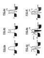
- FIGS. 4a to 4f an operating mode of the device according to the invention, and more particularly a mode of operation of the transistor TR based on the blocking principle of Coulomb.
- the electrostatic energy of a transistor entering the channel is defined by the formula (I) below: e 2 / (2 ⁇ Yes ⁇ 0 d) in which e denotes the charge of an electron, ⁇ Si denotes the permittivity of the silicon and d is the “diameter” of the device which is equal as a first approximation to (WxL) 1/2 .
- the thermal energy is equal to kxT, where k denotes the constant of Boltzmann and T the operating temperature of the device.
- values of L and W respectively equal to 30 nm and 300 nm, suitable for operation at a temperature equal to 4.2 ° K.
- W is very large, for example equal to 1 ⁇ m or 10 ⁇ m
- Coulomb blocking phenomenon
- FIGS. 4a to 4f the profile of the energy in the channel of the transistor is shown.
- E F designates the Fermi level of the source and Vd designates the voltage applied to the drain of the transistor.
- the voltage Vg applied to the gate of the transistor is zero. There is no creation of potential wells. And, the operating temperature of the device is chosen so that that the value of the thermal energy of the electrons is much less than the height of the potential barrier thus defined. Therefore, there is no electron passage and the transistor is blocked.
- the drain voltage must be sufficiently low so that the grid voltage can allow the creation of the double barrier structure allowing Coulomb blocking.
- a voltage of drain less than 10 mV.
- the minimum grid voltage to apply to arrive in the on state of the transistor is the threshold voltage of this transistor, conventionally determined by the thickness of the gate oxide OX, the doping of the channel and the output work of the material serving as the gate electrode.
- the product of this tension of grid Vg0 by the charge e of an electron, must be equal to the energy electrostatic of this electron entering the transistor channel.
- the electron having penetrated into the channel passes through the drain D by tunnel effect, causing the creation of a drain current.
- This electron will then be trapped in one of the boxes quantum BQ and cause the emission of a single photon ph.
- the control means are then able to deliver successively the two values of the control voltage at one working frequency which is higher than the output frequency of a channel electron, in practice between 1 MHz and 1 GHz. This ensures that only one electron comes out at a time.
- the profile of the structure in the conduction band illustrates the operation of the device according to the invention.
- the quantum dots had a yield of conversion equal to 1, the data rate transmitted by such device would be equal to the working frequency f. That said, the conversion yields in a system using materials with non-direct gaps are generally very small. But, this is not annoying in cryptographic applications, since the quantity of information to be transmitted by quantum cryptography can remain relatively small.
- a coding key is coded on 128 bits.
- the number of bits transmitted per second is equal to 0.1, which then requires a time of approximately 20 minutes to transmit a 128-bit key. That said, we can show that using photonic crystals, the quantum efficiency of silicon-based boxes can drop to 10 -3 , which in this case would reduce the transmission time of a 128-bit key at 0.1 seconds.
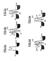
- the energy of the quantified levels is higher to electrostatic energy.
- the condition for an electron to pass from the source to drain is determined by both the alignment of the level fundamental N1 of the quantum well with the Fermi EF level of the source and the electrostatic energy brought by the electron into the channel.
- the application of the grid control voltage allows the creation of a well Quantum.
- the electron which is in the channel can exit by tunnel effect, bringing the system back to an initial state (Figure 5e).
- Determining the blocking condition requires know the value of the energy of the fundamental level N1. Such calculation is well known to those skilled in the art and it depends in particular the shape of the grid, i.e. the length L of the grid base and non-overlapping of the extension zones with the grid, as well as of the profile of the source / channel and channel / drain junction.
- the reference SB designates the silicon substrate, for example P - doped, within which an active zone has been produced delimited in a conventional manner and known per se by STI isolation regions, for example called “trenches” shallow ”.
- an OX thermal oxide is grown on the surface of the substrate.
- the following steps consist in making the transistor with its mushroom-shaped grill.
- the first of them consists in depositing a stack of a lower layer formed for example of a polycrystalline alloy of silicon and germanium, such as Si 0.75 Ge 0.25 , in a thickness for example of 500 ⁇ .
- the lower layer is topped with an upper layer of polysilicon, for example having a thickness of 1000 ⁇ .
- a lateral etching GRL of the lower layer CH2 is carried out until a grid base GP having a length for example equal to 16 nm is obtained.
- GRL etching can be carried out using a chemical solution selective with respect to silicon, such as a 40 ml HNO 3 solution at 70% - 20 ml H 2 O 2 - 5 ml HF 0.5%. Lateral etching can also be carried out by selective isotropic plasma attack with respect to silicon and oxide.
- insulating side panels resting on the sides of the grid.
- These ESP spacers are for example made of silicon nitride ( Figure 7g).
- a second installation is then carried out, so as to form the source and drain regions, the drain region coming contact the ZIM area located under the BQ quantum dots.
- the next step which leads to the device illustrated on Figure 2, includes in particular a photolithography step of so as to define the location of the opening opening above the quantum dots, then an etching of the metal layer and a opening of the orifice above the quantum dots.
- This hole serves waveguide. It could also be filled with silicon.
- the chip containing the device thus produced can then be incorporated in a refrigerated enclosure.
- the whole can then form a cryptography device capable of emitting a train of photons, photon after photon.
Landscapes
- Physics & Mathematics (AREA)
- Engineering & Computer Science (AREA)
- Nanotechnology (AREA)
- Optics & Photonics (AREA)
- Chemical & Material Sciences (AREA)
- Crystallography & Structural Chemistry (AREA)
- Biophysics (AREA)
- Life Sciences & Earth Sciences (AREA)
- Condensed Matter Physics & Semiconductors (AREA)
- General Physics & Mathematics (AREA)
- Electromagnetism (AREA)
- Insulated Gate Type Field-Effect Transistor (AREA)
- Junction Field-Effect Transistors (AREA)
Abstract
Description
- un transistor MOS ayant une grille de forme de champignon, capable de délivrer sur son drain, de façon contrôlée, un électron unique en réponse à une tension de commande appliquée sur sa grille, et
- au moins une boíte quantique compatible silicium, électriquement couplée à la région de drain du transistor, et capable d'émettre un photon unique à la réception d'un électron unique émis par le transistor.
- la figure 1 illustre schématiquement un mode de réalisation d'un dispositif semiconducteur formant source d'un photon unique selon l'invention ;
- la figure 2 illustre schématiquement une représentation du dispositif de la figure 1 sous une forme intégrée ;
- la figure 3 illustre schématiquement un puits quantique formé sous la grille d'un transistor d'un dispositif selon l'invention ;
- les figures 4a à 4f illustrent schématiquement un mode de fonctionnement du dispositif selon l'invention faisant intervenir un blocage de Coulomb ;
- les figures 5a à 5e illustrent un autre mode de fonctionnement du dispositif selon l'invention faisant intervenir un effet tunnel résonant ;
- la figure 6 illustre un profil de la bande de conduction d'un dispositif selon l'invention ; et
- les figures 7a à 7i illustrent schématiquement les principales étapes d'un mode de mise en oeuvre d'un procédé de fabrication selon l'invention.
εSi désigne la permittivité du silicium et d est le « diamètre » du dispositif qui est égal en première approximation à (WxL)1/2.
- de Boucaud, intitulés « Optical recombination from excited states in Ge/Si self-assembled quantum dots », Physical Review B, Volume 64, 155310, et
- de T. Brunhes, et autres, intitulés « Electroluminescence of Ge/Si self-assembled quantum dots grown by chemical vapor deposition » (Applied Physics Letters, Volume 77, N°12, 18 septembre 2000, en ont montré un exemple de réalisation.
Claims (25)
- Circuit intégré, comprenant un dispositif semiconducteur formant source à photon unique, comportant sur un substrat en silicium (SB) un transistor MOS (TR) ayant une grille en forme de champignon, capable de délivrer sur son drain, de façon contrôlée, un électron unique en réponse à une tension de commande appliquée sur sa grille, et au moins une boíte quantique (BQ) compatible silicium, électriquement couplée à la région de drain (D) du transistor, et capable d'émettre un photon unique à la réception d'un électron unique émis par le transistor.
- Circuit intégré selon la revendication 1, caractérisé par le fait que la grille (G) du transistor comporte un pied de grille (GP) ayant une longueur L et une largeur W, surmonté d'un chapeau (GCH), des régions isolantes latérales (ESP) sur les flancs de la grille, et des régions de source et de drain situées dans le substrat à distance des bords latéraux du pied de grille.
- Circuit intégré selon la revendication 2, caractérisé par le fait que les valeurs de L et de W sont choisies de sorte que l'énergie thermique des électrons dans la source du transistor (TR) soit inférieure à l'énergie électrostatique d'un électron pénétrant dans le canal du transistor.
- Circuit intégré selon la revendication 3, caractérisé par le fait que la température de fonctionnement du dispositif est inférieure à 77°K et par le fait que L est inférieur à 50 nanomètres.
- Circuit intégré selon la revendication 3 ou 4, caractérisé par le fait que W est inférieur à quelques centaines de nanomètres, par exemple 500 nanomètres.
- Circuit intégré selon l'une des revendications précédentes, caractérisé par le fait que la tension appliquée sur le drain (D) du transistor est inférieure à 10 mV.
- Circuit intégré selon l'une des revendications précédentes, caractérisé par le fait qu'il comporte des moyens de commande (MCG) aptes à délivrer ladite tension de commande, cette tension de commande ayant une première valeur au moins nulle en réponse à laquelle le transistor est bloqué, et une deuxième valeur permettant la création d'un puits quantique dans le canal du transistor et le passage d'un électron unique de la source dans le canal puis vers le drain.
- Circuit intégré selon les revendications 2 et 7, caractérisé par le fait que L est supérieur ou égal à 10 nanomètres et inférieur à 50 nanomètres, et par le fait que le produit de la deuxième valeur de la tension de commande par la charge (e) d'un électron est un multiple entier de l'énergie électrostatique d'un électron pénétrant dans le canal du transistor.
- Circuit intégré selon la revendication 8, caractérisé par le fait que le produit de la deuxième valeur de la tension de commande par la charge (e) d'un électron est égal à l'énergie électrostatique d'un électron pénétrant dans le canal du transistor.
- Circuit intégré selon les revendications 2 et 7, caractérisé par le fait que L inférieur à 10 nanomètres, et par le fait que la deuxième valeur de la tension de commande correspond à un alignement du niveau fondamental d'énergie du dispositif avec le niveau de Fermi de la source du transistor.
- Circuit intégré selon l'une des revendications 7 à 10, caractérisé par le fait que les moyens de commande (MCG) sont aptes à délivrer successivement les deux valeurs de la tension de commande à une fréquence de travail (f) supérieure à la fréquence de sortie d'un électron du canal.
- Circuit intégré selon la revendication 11, caractérisé par le fait que la fréquence de travail (f) est comprise entre 1 MHz et 1 GHz.
- Circuit intégré selon l'une des revendications précédentes, caractérisé par le fait que le dispositif comporte plusieurs boítes quantiques adjacentes (BQ).
- Circuit intégré selon l'une des revendications précédentes, caractérisé par le fait que le substrat (SB) comporte une région implantée supplémentaire (ZIM), située sous chaque boíte quantique, de même type de conductivité que celui de la région de drain, et en contact avec la région de drain.
- Circuit intégré selon l'une des revendications précédentes, caractérisé par le fait que chaque boíte quantique (BQ) comporte du germanium encapsulé dans du silicium.
- Circuit intégré selon l'une des revendications précédentes, caractérisé par le fait que le dispositif comporte une couche de matériau isolant (ENR) enrobant le transistor, cette couche de matériau isolant comportant un orifice débouchant au dessus des boítes quantiques et formant un guide d'ondes optique (GUD).
- Circuit intégré selon l'une des revendications précédentes, caractérisé par le fait qu'il est disposé dans une enceinte réfrigérée.
- Dispositif de cryptographie, caractérisé par le fait qu'il comporte un circuit intégré selon l'une des revendications 1 à 17.
- Procédé de fabrication d'un circuit intégré comprenant un dispositif semiconducteur formant source à photon unique, dans lequel on réalise dans et sur un substrat en silicium (SR), un transistor MOS (TR) ayant une grille en forme de champignon, capable de délivrer sur son drain, de façon contrôlée, un électron unique en réponse à une tension de commande appliquée sur sa grille, et au moins une boíte quantique (BQ) compatible silicium, électriquement couplée à la région de drain du transistor, et capable d'émettre un photon unique à la réception d'un électron unique émis par le transistor.
- Procédé selon la revendication 19, caractérisé par le fait qu'on réalise plusieurs boítes quantiques adjacentes (BQ), et par le fait que réalisation comporte une croissance sélective de germanium sur la surface d'une première région prédéterminée du substrat, puis une croissance sélective de silicium sur le germanium.
- Procédé selon la revendication 19 ou 20, caractérisé par le fait que la réalisation du transistor comporte la formation sur la surface d'une deuxième région prédéterminée du substrat d'un corps de grille (CRG) isolée de ladite surface par un oxyde de grille (OX), puis une gravure latérale du corps de grille de façon à former un pied de grille surmonté d'un chapeau.
- Procédé selon la revendication 21, caractérisé par le fait que le corps de grille est un empilement hétérogène comprenant une couche inférieure (CH2) et une couche supérieure (CH1), le matériau de la couche supérieure pouvant être gravé sélectivement par rapport au matériau de la couche supérieure.
- Procédé selon la revendication 22, caractérisé par le fait que le matériau de la couche inférieure (CH2) est un alliage de silicium et de germanium, tandis que matériau de la couche supérieure (CH1) est du silicium.
- Procédé selon l'une des revendications 21 à 23, caractérisé par le fait que les régions de source et de drain sont implantées dans le substrat en utilisant le chapeau de grille comme masque dur.
- Procédé d'émission d'un photon unique, comportant une application sur la grille en forme de champignon d'un transistor MOS, d'une tension de commande de façon à générer un unique électron au niveau du drain du transistor, et un piégeage de cet électron unique dans une boíte quantique provoquant l'émission d'un photon unique.
Applications Claiming Priority (2)
| Application Number | Priority Date | Filing Date | Title |
|---|---|---|---|
| FR0205539 | 2002-05-03 | ||
| FR0205539A FR2839388A1 (fr) | 2002-05-03 | 2002-05-03 | Procede d'emission d'un photon unique, dispositif semiconducteur et procede de fabrication correspondant |
Publications (2)
| Publication Number | Publication Date |
|---|---|
| EP1363372A1 true EP1363372A1 (fr) | 2003-11-19 |
| EP1363372B1 EP1363372B1 (fr) | 2007-06-06 |
Family
ID=29226158
Family Applications (1)
| Application Number | Title | Priority Date | Filing Date |
|---|---|---|---|
| EP03291031A Expired - Lifetime EP1363372B1 (fr) | 2002-05-03 | 2003-04-28 | Procédé d'émission d'un photon unique, dispositif semiconducteur et procédé de fabrication correspondants |
Country Status (4)
| Country | Link |
|---|---|
| US (1) | US6852993B2 (fr) |
| EP (1) | EP1363372B1 (fr) |
| DE (1) | DE60314203D1 (fr) |
| FR (1) | FR2839388A1 (fr) |
Families Citing this family (2)
| Publication number | Priority date | Publication date | Assignee | Title |
|---|---|---|---|---|
| US9859409B2 (en) * | 2016-04-28 | 2018-01-02 | International Business Machines Corporation | Single-electron transistor with wrap-around gate |
| GB201703594D0 (en) * | 2017-03-07 | 2017-04-19 | Univ Of Lancaster | Single photon source |
Citations (1)
| Publication number | Priority date | Publication date | Assignee | Title |
|---|---|---|---|---|
| WO2001093384A1 (fr) * | 2000-05-29 | 2001-12-06 | France Telecom | Source a un photon a base d'emetteurs dont les frequences sont reparties de maniere choisie |
Family Cites Families (4)
| Publication number | Priority date | Publication date | Assignee | Title |
|---|---|---|---|---|
| US6720589B1 (en) * | 1998-09-16 | 2004-04-13 | Kabushiki Kaisha Toshiba | Semiconductor device |
| JP4029420B2 (ja) * | 1999-07-15 | 2008-01-09 | 独立行政法人科学技術振興機構 | ミリ波・遠赤外光検出器 |
| ATE342584T1 (de) * | 1999-08-19 | 2006-11-15 | Hitachi Europ Ltd | Photodetektor |
| US6728281B1 (en) * | 2000-02-10 | 2004-04-27 | The Board Of Trustees Of The Leland Stanford Junior University | Quantum-dot photon turnstile device |
-
2002
- 2002-05-03 FR FR0205539A patent/FR2839388A1/fr active Pending
-
2003
- 2003-04-28 DE DE60314203T patent/DE60314203D1/de not_active Expired - Lifetime
- 2003-04-28 EP EP03291031A patent/EP1363372B1/fr not_active Expired - Lifetime
- 2003-05-05 US US10/429,908 patent/US6852993B2/en not_active Expired - Lifetime
Patent Citations (1)
| Publication number | Priority date | Publication date | Assignee | Title |
|---|---|---|---|---|
| WO2001093384A1 (fr) * | 2000-05-29 | 2001-12-06 | France Telecom | Source a un photon a base d'emetteurs dont les frequences sont reparties de maniere choisie |
Non-Patent Citations (2)
| Title |
|---|
| BOEUF F ET AL: "16 nm planar NMOSFET manufacturable within state-of-the-art CMOS process thanks to specific design and optimisation", INTERNATIONAL ELECTRON DEVICES MEETING. TECHNICAL DIGEST (CAT. NO.01CH37224), INTERNATIONAL ELECTRON DEVICES MEETING. TECHNICAL DIGEST, WASHINGTON, DC, USA, 2-5 DEC. 2001, 2001, Piscataway, NJ, USA, IEEE, USA, pages 29.5.1 - 4, XP002237153, ISBN: 0-7803-7050-3 * |
| MOREAU E ET AL: "Single-mode solid-state single photon source based on isolated quantum dots in pillar microcavities", APPLIED PHYSICS LETTERS, 29 OCT. 2001, AIP, USA, vol. 79, no. 18, pages 2865 - 2867, XP002237154, ISSN: 0003-6951 * |
Also Published As
| Publication number | Publication date |
|---|---|
| EP1363372B1 (fr) | 2007-06-06 |
| US20030218163A1 (en) | 2003-11-27 |
| FR2839388A1 (fr) | 2003-11-07 |
| US6852993B2 (en) | 2005-02-08 |
| DE60314203D1 (de) | 2007-07-19 |
Similar Documents
| Publication | Publication Date | Title |
|---|---|---|
| EP0852814B1 (fr) | Transistor mos a puits quantique et procedes de fabrication de celui-ci | |
| US7838894B2 (en) | Optical device having photoelectric conversion layer | |
| EP0887866B1 (fr) | Dispositif semiconducteur comprenant un agrégat de micro-aiguilles semi-conductrices | |
| FR3072834A1 (fr) | Dispositifs a semi-conducteur contraint en tension de detection et d'emission photonique et systeme photonique integre | |
| US20110073989A1 (en) | Optical modulator utilizing wafer bonding technology | |
| FR2655434A1 (fr) | Dispositif optique a puits quantiques et procede de realisation. | |
| EP3145038A1 (fr) | Structure de laser à nanofil et son procédé de fabrication | |
| EP2337094B1 (fr) | Source de photons résultants d'une recombinaison d'excitons localisés | |
| US7180648B2 (en) | Electro-absorption modulator device and methods for fabricating the same | |
| EP1138101B1 (fr) | Laser de type semi-conducteur | |
| FR2858717A1 (fr) | Procede de fabrication d'une cellule auto-alignee du type silicium-oxyde-nitrure-oxyde-silicium et cette cellule | |
| EP4009456B1 (fr) | Procédé de réalisation d'un miroir de bragg distribué | |
| EP1363372B1 (fr) | Procédé d'émission d'un photon unique, dispositif semiconducteur et procédé de fabrication correspondants | |
| FR2907916A1 (fr) | Nouvelle structure de guide a fente | |
| EP3660921A1 (fr) | Procédé de fabrication d'un composant électronique à multiples îlots quantiques et composant électronique résultant | |
| EP0684653B1 (fr) | Composant à hétérostructure semi-conductrice, commandé par la lumière pour la génération d'oscillations hyperfréquences | |
| EP4033540A1 (fr) | Dispositif comprenant des grilles de commande électrostatique reparties sur deux faces opposées d'une portion de semiconducteur | |
| EP4386634A1 (fr) | Electrodes d'échange pour réseau d'ilots quantiques | |
| US20040017600A1 (en) | Electroabsorption modulator, modulator laser device and method for producing an electroabsorption modulator | |
| EP4271165B1 (fr) | Procede de realisation d'un dispositif electronique a qubit(s) supraconducteur(s) incluant au moins un jofet | |
| KR20080042853A (ko) | 반도체 구조체 및 광 생성 방법 | |
| EP4185093B1 (fr) | Procédé de réalisation d'un dispositif quantique | |
| JP2014183055A (ja) | 発光素子及びその製造方法 | |
| US5589404A (en) | Monolithically integrated VLSI optoelectronic circuits and a method of fabricating the same | |
| FR2982419A1 (fr) | Dispositif emetteur de rayonnement lumineux a transistors de type p et de type n tete-beche |
Legal Events
| Date | Code | Title | Description |
|---|---|---|---|
| PUAI | Public reference made under article 153(3) epc to a published international application that has entered the european phase |
Free format text: ORIGINAL CODE: 0009012 |
|
| AK | Designated contracting states |
Kind code of ref document: A1 Designated state(s): AT BE BG CH CY CZ DE DK EE ES FI FR GB GR HU IE IT LI LU MC NL PT RO SE SI SK TR |
|
| AX | Request for extension of the european patent |
Extension state: AL LT LV MK |
|
| RIN1 | Information on inventor provided before grant (corrected) |
Inventor name: DUTARTRE, DIDIER Inventor name: BOEUF, FREDERIC Inventor name: MONFRAY, STEPHANE |
|
| 17P | Request for examination filed |
Effective date: 20040422 |
|
| AKX | Designation fees paid |
Designated state(s): DE FR GB IT |
|
| GRAP | Despatch of communication of intention to grant a patent |
Free format text: ORIGINAL CODE: EPIDOSNIGR1 |
|
| GRAS | Grant fee paid |
Free format text: ORIGINAL CODE: EPIDOSNIGR3 |
|
| GRAA | (expected) grant |
Free format text: ORIGINAL CODE: 0009210 |
|
| AK | Designated contracting states |
Kind code of ref document: B1 Designated state(s): DE FR GB IT |
|
| REG | Reference to a national code |
Ref country code: GB Ref legal event code: FG4D Free format text: NOT ENGLISH |
|
| REF | Corresponds to: |
Ref document number: 60314203 Country of ref document: DE Date of ref document: 20070719 Kind code of ref document: P |
|
| GBT | Gb: translation of ep patent filed (gb section 77(6)(a)/1977) |
Effective date: 20070813 |
|
| PLBE | No opposition filed within time limit |
Free format text: ORIGINAL CODE: 0009261 |
|
| STAA | Information on the status of an ep patent application or granted ep patent |
Free format text: STATUS: NO OPPOSITION FILED WITHIN TIME LIMIT |
|
| PG25 | Lapsed in a contracting state [announced via postgrant information from national office to epo] |
Ref country code: IT Free format text: LAPSE BECAUSE OF FAILURE TO SUBMIT A TRANSLATION OF THE DESCRIPTION OR TO PAY THE FEE WITHIN THE PRESCRIBED TIME-LIMIT Effective date: 20070606 Ref country code: DE Free format text: LAPSE BECAUSE OF FAILURE TO SUBMIT A TRANSLATION OF THE DESCRIPTION OR TO PAY THE FEE WITHIN THE PRESCRIBED TIME-LIMIT Effective date: 20070907 |
|
| 26N | No opposition filed |
Effective date: 20080307 |
|
| PGFP | Annual fee paid to national office [announced via postgrant information from national office to epo] |
Ref country code: GB Payment date: 20080326 Year of fee payment: 6 |
|
| GBPC | Gb: european patent ceased through non-payment of renewal fee |
Effective date: 20090428 |
|
| REG | Reference to a national code |
Ref country code: FR Ref legal event code: ST Effective date: 20091231 |
|
| PG25 | Lapsed in a contracting state [announced via postgrant information from national office to epo] |
Ref country code: FR Free format text: LAPSE BECAUSE OF NON-PAYMENT OF DUE FEES Effective date: 20091222 Ref country code: GB Free format text: LAPSE BECAUSE OF NON-PAYMENT OF DUE FEES Effective date: 20090428 |
|
| PGFP | Annual fee paid to national office [announced via postgrant information from national office to epo] |
Ref country code: FR Payment date: 20080429 Year of fee payment: 6 |