EP1363369B1 - Monolithic multi-wavelength vertical-cavity surface emitting laser array and method of manufacture therefor - Google Patents
Monolithic multi-wavelength vertical-cavity surface emitting laser array and method of manufacture therefor Download PDFInfo
- Publication number
- EP1363369B1 EP1363369B1 EP03002337A EP03002337A EP1363369B1 EP 1363369 B1 EP1363369 B1 EP 1363369B1 EP 03002337 A EP03002337 A EP 03002337A EP 03002337 A EP03002337 A EP 03002337A EP 1363369 B1 EP1363369 B1 EP 1363369B1
- Authority
- EP
- European Patent Office
- Prior art keywords
- reflector
- forming
- vertical cavity
- optical devices
- different
- Prior art date
- Legal status (The legal status is an assumption and is not a legal conclusion. Google has not performed a legal analysis and makes no representation as to the accuracy of the status listed.)
- Expired - Lifetime
Links
- 238000000034 method Methods 0.000 title claims description 28
- 238000004519 manufacturing process Methods 0.000 title claims description 18
- 239000004065 semiconductor Substances 0.000 claims description 48
- 230000003287 optical effect Effects 0.000 claims description 37
- 239000000463 material Substances 0.000 description 27
- 230000012010 growth Effects 0.000 description 14
- VYPSYNLAJGMNEJ-UHFFFAOYSA-N Silicium dioxide Chemical compound O=[Si]=O VYPSYNLAJGMNEJ-UHFFFAOYSA-N 0.000 description 10
- 238000005530 etching Methods 0.000 description 7
- 239000000758 substrate Substances 0.000 description 7
- GWEVSGVZZGPLCZ-UHFFFAOYSA-N Titan oxide Chemical compound O=[Ti]=O GWEVSGVZZGPLCZ-UHFFFAOYSA-N 0.000 description 6
- 238000000151 deposition Methods 0.000 description 5
- 239000003989 dielectric material Substances 0.000 description 5
- 239000000377 silicon dioxide Substances 0.000 description 5
- IJGRMHOSHXDMSA-UHFFFAOYSA-N Atomic nitrogen Chemical compound N#N IJGRMHOSHXDMSA-UHFFFAOYSA-N 0.000 description 4
- 238000003491 array Methods 0.000 description 4
- 229910052681 coesite Inorganic materials 0.000 description 4
- 229910052906 cristobalite Inorganic materials 0.000 description 4
- 230000008021 deposition Effects 0.000 description 4
- 229910052751 metal Inorganic materials 0.000 description 4
- 239000002184 metal Substances 0.000 description 4
- 229910052682 stishovite Inorganic materials 0.000 description 4
- 229910052905 tridymite Inorganic materials 0.000 description 4
- 229910052581 Si3N4 Inorganic materials 0.000 description 3
- 229910052782 aluminium Inorganic materials 0.000 description 3
- XAGFODPZIPBFFR-UHFFFAOYSA-N aluminium Chemical compound [Al] XAGFODPZIPBFFR-UHFFFAOYSA-N 0.000 description 3
- 238000004544 sputter deposition Methods 0.000 description 3
- GYHNNYVSQQEPJS-UHFFFAOYSA-N Gallium Chemical compound [Ga] GYHNNYVSQQEPJS-UHFFFAOYSA-N 0.000 description 2
- PNEYBMLMFCGWSK-UHFFFAOYSA-N aluminium oxide Inorganic materials [O-2].[O-2].[O-2].[Al+3].[Al+3] PNEYBMLMFCGWSK-UHFFFAOYSA-N 0.000 description 2
- 238000013459 approach Methods 0.000 description 2
- 229910052785 arsenic Inorganic materials 0.000 description 2
- RQNWIZPPADIBDY-UHFFFAOYSA-N arsenic atom Chemical compound [As] RQNWIZPPADIBDY-UHFFFAOYSA-N 0.000 description 2
- 238000004891 communication Methods 0.000 description 2
- 229910052593 corundum Inorganic materials 0.000 description 2
- 229910052733 gallium Inorganic materials 0.000 description 2
- BHEPBYXIRTUNPN-UHFFFAOYSA-N hydridophosphorus(.) (triplet) Chemical compound [PH] BHEPBYXIRTUNPN-UHFFFAOYSA-N 0.000 description 2
- 229910052738 indium Inorganic materials 0.000 description 2
- APFVFJFRJDLVQX-UHFFFAOYSA-N indium atom Chemical compound [In] APFVFJFRJDLVQX-UHFFFAOYSA-N 0.000 description 2
- 238000000869 ion-assisted deposition Methods 0.000 description 2
- 230000000873 masking effect Effects 0.000 description 2
- 238000012986 modification Methods 0.000 description 2
- 230000004048 modification Effects 0.000 description 2
- 229910003465 moissanite Inorganic materials 0.000 description 2
- 229910052757 nitrogen Inorganic materials 0.000 description 2
- 229920000620 organic polymer Polymers 0.000 description 2
- 238000000059 patterning Methods 0.000 description 2
- 238000012545 processing Methods 0.000 description 2
- HBMJWWWQQXIZIP-UHFFFAOYSA-N silicon carbide Chemical compound [Si+]#[C-] HBMJWWWQQXIZIP-UHFFFAOYSA-N 0.000 description 2
- 229910010271 silicon carbide Inorganic materials 0.000 description 2
- HQVNEWCFYHHQES-UHFFFAOYSA-N silicon nitride Chemical compound N12[Si]34N5[Si]62N3[Si]51N64 HQVNEWCFYHHQES-UHFFFAOYSA-N 0.000 description 2
- 229910001845 yogo sapphire Inorganic materials 0.000 description 2
- 239000004642 Polyimide Substances 0.000 description 1
- XUIMIQQOPSSXEZ-UHFFFAOYSA-N Silicon Chemical compound [Si] XUIMIQQOPSSXEZ-UHFFFAOYSA-N 0.000 description 1
- 230000003321 amplification Effects 0.000 description 1
- QVGXLLKOCUKJST-UHFFFAOYSA-N atomic oxygen Chemical compound [O] QVGXLLKOCUKJST-UHFFFAOYSA-N 0.000 description 1
- 230000005540 biological transmission Effects 0.000 description 1
- 230000001419 dependent effect Effects 0.000 description 1
- 238000001704 evaporation Methods 0.000 description 1
- 230000008020 evaporation Effects 0.000 description 1
- 239000000835 fiber Substances 0.000 description 1
- 239000007789 gas Substances 0.000 description 1
- PCHJSUWPFVWCPO-UHFFFAOYSA-N gold Chemical compound [Au] PCHJSUWPFVWCPO-UHFFFAOYSA-N 0.000 description 1
- 229910052737 gold Inorganic materials 0.000 description 1
- 239000010931 gold Substances 0.000 description 1
- 238000001459 lithography Methods 0.000 description 1
- 238000001451 molecular beam epitaxy Methods 0.000 description 1
- 238000003199 nucleic acid amplification method Methods 0.000 description 1
- 239000013307 optical fiber Substances 0.000 description 1
- 239000001301 oxygen Substances 0.000 description 1
- 229910052760 oxygen Inorganic materials 0.000 description 1
- 238000000206 photolithography Methods 0.000 description 1
- 229920001721 polyimide Polymers 0.000 description 1
- 238000002310 reflectometry Methods 0.000 description 1
- 239000010703 silicon Substances 0.000 description 1
- 235000012239 silicon dioxide Nutrition 0.000 description 1
- 229910052814 silicon oxide Inorganic materials 0.000 description 1
Images

Classifications
-
- H—ELECTRICITY
- H01—ELECTRIC ELEMENTS
- H01S—DEVICES USING THE PROCESS OF LIGHT AMPLIFICATION BY STIMULATED EMISSION OF RADIATION [LASER] TO AMPLIFY OR GENERATE LIGHT; DEVICES USING STIMULATED EMISSION OF ELECTROMAGNETIC RADIATION IN WAVE RANGES OTHER THAN OPTICAL
- H01S5/00—Semiconductor lasers
- H01S5/40—Arrangement of two or more semiconductor lasers, not provided for in groups H01S5/02 - H01S5/30
- H01S5/42—Arrays of surface emitting lasers
- H01S5/423—Arrays of surface emitting lasers having a vertical cavity
-
- H—ELECTRICITY
- H01—ELECTRIC ELEMENTS
- H01S—DEVICES USING THE PROCESS OF LIGHT AMPLIFICATION BY STIMULATED EMISSION OF RADIATION [LASER] TO AMPLIFY OR GENERATE LIGHT; DEVICES USING STIMULATED EMISSION OF ELECTROMAGNETIC RADIATION IN WAVE RANGES OTHER THAN OPTICAL
- H01S5/00—Semiconductor lasers
- H01S5/10—Construction or shape of the optical resonator, e.g. extended or external cavity, coupled cavities, bent-guide, varying width, thickness or composition of the active region
- H01S5/18—Surface-emitting [SE] lasers, e.g. having both horizontal and vertical cavities
- H01S5/183—Surface-emitting [SE] lasers, e.g. having both horizontal and vertical cavities having only vertical cavities, e.g. vertical cavity surface-emitting lasers [VCSEL]
- H01S5/18341—Intra-cavity contacts
-
- H—ELECTRICITY
- H01—ELECTRIC ELEMENTS
- H01S—DEVICES USING THE PROCESS OF LIGHT AMPLIFICATION BY STIMULATED EMISSION OF RADIATION [LASER] TO AMPLIFY OR GENERATE LIGHT; DEVICES USING STIMULATED EMISSION OF ELECTROMAGNETIC RADIATION IN WAVE RANGES OTHER THAN OPTICAL
- H01S5/00—Semiconductor lasers
- H01S5/10—Construction or shape of the optical resonator, e.g. extended or external cavity, coupled cavities, bent-guide, varying width, thickness or composition of the active region
- H01S5/18—Surface-emitting [SE] lasers, e.g. having both horizontal and vertical cavities
- H01S5/183—Surface-emitting [SE] lasers, e.g. having both horizontal and vertical cavities having only vertical cavities, e.g. vertical cavity surface-emitting lasers [VCSEL]
- H01S5/18358—Surface-emitting [SE] lasers, e.g. having both horizontal and vertical cavities having only vertical cavities, e.g. vertical cavity surface-emitting lasers [VCSEL] containing spacer layers to adjust the phase of the light wave in the cavity
-
- H—ELECTRICITY
- H01—ELECTRIC ELEMENTS
- H01S—DEVICES USING THE PROCESS OF LIGHT AMPLIFICATION BY STIMULATED EMISSION OF RADIATION [LASER] TO AMPLIFY OR GENERATE LIGHT; DEVICES USING STIMULATED EMISSION OF ELECTROMAGNETIC RADIATION IN WAVE RANGES OTHER THAN OPTICAL
- H01S5/00—Semiconductor lasers
- H01S5/10—Construction or shape of the optical resonator, e.g. extended or external cavity, coupled cavities, bent-guide, varying width, thickness or composition of the active region
- H01S5/18—Surface-emitting [SE] lasers, e.g. having both horizontal and vertical cavities
- H01S5/183—Surface-emitting [SE] lasers, e.g. having both horizontal and vertical cavities having only vertical cavities, e.g. vertical cavity surface-emitting lasers [VCSEL]
- H01S5/18361—Structure of the reflectors, e.g. hybrid mirrors
- H01S5/18363—Structure of the reflectors, e.g. hybrid mirrors comprising air layers
- H01S5/18366—Membrane DBR, i.e. a movable DBR on top of the VCSEL
-
- H—ELECTRICITY
- H01—ELECTRIC ELEMENTS
- H01S—DEVICES USING THE PROCESS OF LIGHT AMPLIFICATION BY STIMULATED EMISSION OF RADIATION [LASER] TO AMPLIFY OR GENERATE LIGHT; DEVICES USING STIMULATED EMISSION OF ELECTROMAGNETIC RADIATION IN WAVE RANGES OTHER THAN OPTICAL
- H01S5/00—Semiconductor lasers
- H01S5/10—Construction or shape of the optical resonator, e.g. extended or external cavity, coupled cavities, bent-guide, varying width, thickness or composition of the active region
- H01S5/18—Surface-emitting [SE] lasers, e.g. having both horizontal and vertical cavities
- H01S5/183—Surface-emitting [SE] lasers, e.g. having both horizontal and vertical cavities having only vertical cavities, e.g. vertical cavity surface-emitting lasers [VCSEL]
- H01S5/18361—Structure of the reflectors, e.g. hybrid mirrors
- H01S5/18369—Structure of the reflectors, e.g. hybrid mirrors based on dielectric materials
-
- H—ELECTRICITY
- H01—ELECTRIC ELEMENTS
- H01S—DEVICES USING THE PROCESS OF LIGHT AMPLIFICATION BY STIMULATED EMISSION OF RADIATION [LASER] TO AMPLIFY OR GENERATE LIGHT; DEVICES USING STIMULATED EMISSION OF ELECTROMAGNETIC RADIATION IN WAVE RANGES OTHER THAN OPTICAL
- H01S5/00—Semiconductor lasers
- H01S5/40—Arrangement of two or more semiconductor lasers, not provided for in groups H01S5/02 - H01S5/30
- H01S5/4025—Array arrangements, e.g. constituted by discrete laser diodes or laser bar
- H01S5/4087—Array arrangements, e.g. constituted by discrete laser diodes or laser bar emitting more than one wavelength
Definitions
- the present invention relates generally to vertical cavity lasers, and more specifically to monolithic arrays of vertical cavity lasers.
- VSELs Vertical cavity surface emitting lasers
- VCSELs are semiconductor devices, which are revolutionizing the field of telecommunications. They generally consist of a pair of semiconductor mirrors defining a resonant cavity containing a gain medium of semiconductor materials for amplifying light.
- VCSELs have relatively high efficiency, small size, low weight, low power consumption, and the capability to be driven by low-voltage power. They can operate in a single longitudinal mode, or frequency, and produce a circular beam of laser light that can easily be coupled into optical fibers.
- the surface emission feature allows devices to be packed densely on a wafer, so that two-dimensional arrays are fabricated relatively easily.
- VCSELS use semiconductor materials comprised of elements such as aluminum, indium, gallium, arsenic, nitrogen, and phosphorous as the gain medium, and alternating high and low index of refraction materials such as silicon and silicon dioxide for the semiconductor mirrors or distributed Bragg reflectors (DBRs).
- elements such as aluminum, indium, gallium, arsenic, nitrogen, and phosphorous
- alternating high and low index of refraction materials such as silicon and silicon dioxide for the semiconductor mirrors or distributed Bragg reflectors (DBRs).
- DBRs distributed Bragg reflectors
- the lasing wavelength of a VCSEL is determined by the optical height of its resonant cavity. Most commonly the optical height, and thus the wavelength, is determined by the thicknesses of the semiconductor layers in the devices. These thicknesses are set during the growth of the semiconductor layers and are nominally the same for all the VCSELs on given wafer.
- the resonant cavity of some VCSELs also includes an air gap, where the size of the air gap partly determines the lasing wavelength.
- a monolithic multiple-wavelength VCSEL array requires side-by-side fabrication of VCSELs on a wafer where the VCSELs need to be exactly the same except with controlled, different lasing wavelengths. This presents a problem because the processing used on the wafer must assure that the threshold gain at which lasing begins, the current usage, the efficiency, the losses of light in the resonant cavity, the amplification of the gain material, and the light transmission of the DBR all remain the same. At the same time, the same processing must produce different lasing wavelengths, which is most commonly realized by changing the optical height of the resonant cavity.
- One prior art method to making a monolithic multiple wavelength VCSEL array is non-uniform growth due to thermal gradient.
- the backside of a substrate is patterned prior to epitaxial growth in a molecular beam epitaxy reactor.
- the resulting backside pattern produces a thermal gradient on the surface of the substrate when the wafer is heated.
- growth rate is temperature dependent, there is a variable material thickness and hence a variable laser wavelength along the thermal gradient.
- One disadvantage of this approach is the fact that the arrays are limited to linear geometries. To date, there have been problems controlling the wavelengths precisely and repeatedly over large areas of the wafer.
- An alternate prior art method is laterally confining each laser prior to epitaxial growth by either etching a mesa or patterning windows in an oxide mask. This process is known as "selective area growth". Growth rate and composition are functions of the lateral dimension. The method is problematic because it is sensitive to growth conditions and may vary from reactor to reactor or from growth to growth. In both of the aforementioned prior art methods, the proximity of different wavelength devices in an array is limited.
- Another prior art method is to grow a partial VCSEL structure including the lower DBR, the gain material, and some part of the upper DBR.
- the wafer is masked and anodically oxidized to some controlled oxide thickness over the exposed portions.
- a selective etch is then used to remove the oxide. This process is repeated to create different effective resonant cavity lengths for each laser in an array.
- the remainder of the VCSEL structure is regrown over the patterned wafer.
- each etch is sensitive to voltage and concentration variations that cause problems, which affect the depth, resulting in reduced control over wavelength spacing between devices.
- Another prior art method is to grow a partial VCSEL structure including the lower DBR, the gain material, and a series of etch-stop layers that can be selectively etched away.
- the wafer is repeatedly masked and etched so that different amounts of material are removed from the different VCSELs in the array.
- the wafer is then re-introduced into the semiconductor growth apparatus and the deposition of the remaining layers is performed.
- This approach requires multiple masking and etching steps to achieve the different etch depths. This becomes unmanageable when the number of VCSELs is greater than a few.
- this process requires the upper portion of the semiconductor material must be epitaxially re-grown after the etching process is complete. This increases both the complexity and the cost of the fabrication process.
- the present invention provides a monolithic array of vertical cavity lasers with different emission wavelengths on a single wafer, and method of manufacture therefor.
- a first reflector is over the semiconductor substrate with a photoactive semiconductor layer.
- a reflector support defines first and second air gaps with the photoactive semiconductor layer. The second and third air gaps are made to be different from each other by geometric differences in the reflector support structure.
- Second and third reflectors are formed over the reflector support whereby a first laser is formed by the first reflector, the photoactive semiconductor structure, the first air gap, and the second reflector and whereby a second laser is formed by the first reflector, the photoactive semiconductor structure, the second air gap, and the third reflector.
- the emission wavelengths of the first and second lasers are different because of the different sizes of the first and second air gaps. Only one mask is required to set the air gaps for an array containing an arbitrary number of lasers.
- the vertical resonant cavity device is referred to as a vertical cavity optical device (VCOD).
- VCOD vertical cavity optical device
- the invention can also be used to make monolithic arrays of detectors, Fabry-Perot filters, or other optical devices that require a range of resonant cavity wavelengths within the array.
- the term “horizontal” as used in herein is defined as a plane parallel to the conventional plane or surface of a wafer upon which the VCODs are formed regardless of the orientation of the wafer.
- the term “vertical” or “thickness” refers to a direction perpendicular to the horizontal as just defined. Terms, such as “on”, “above”, “below”, “upper”, “lower”, “over”, and “under”, are defined with respect to the horizontal plane. The descriptions of the positions of the various elements in the various embodiments are not intended to be limiting and many other positions would be evident to those skilled in the art.
- FIG. 1 PRIOR ART
- a cross-sectional view of a prior art vertical cavity surface emitting laser or VCSEL 20 Above the substrate 22 is a lower mirror or distributed Bragg reflector (DBR) 24, which consists of a plurality of alternating high and low index of refraction materials.
- the DBR 24 can be made from a number of different combinations of materials including semiconductor layers, dielectric materials such as TiO 2 and SiO 2 , or hybrid combinations of semiconductor, dielectric and metal layers . Each of the layers has an optical thickness of ⁇ 1/4 of a wavelength and the layers are combined until the DBR 24 has an overall reflectance of almost 100%.
- DBR distributed Bragg reflector
- a vertical resonant cavity 26 which consists of a photoactive semiconductor structure 28 and an air gap 30.
- the photoactive semiconductor structure contains a quantum well or quantum wells for providing laser light.
- the air gap 30 is the space above the photoactive semiconductor structure 28 and below a reflector support 32 and held by an anchor 34.
- the heights or thicknesses of the photoactive semiconductor structure 28, the air gap 30, and the reflector support 32 are chosen so their optical thickness are approximately multiples of ⁇ /4 so the vertical resonant cavity 26 has a total height, which is an integral multiple of ⁇ /2.
- the reflector support 32 can be made of a material such as silicon nitride, an organic polymer, or it can be a semiconductor material.
- Mounted on and above the reflector support 32 is an upper mirror or DBR 36, comprised of alternating layers of ⁇ /4 thick low and high index of refraction materials that reflect light from the DBR 36 back to the DBR 24.
- the DBRs 24 and 36 Depending upon the relative reflectivity of the DBRs 24 and 36, light will be emitted upward through the DBR 36 or downward through the DBR 24 and the substrate 22.
- the wavelength of the light will be the same for all VCSELs on the same wafer and a different wavelength will require a different wafer where the vertical resonant cavities will all be of a different height.
- FIG. 2 therein is shown a schematic illustration of how an optical communication system 50 is assembled according to the present invention.
- a single wafer 52 is processed according to the present invention so a plurality of VCODs is formed having different vertical resonant cavities.
- the wafer 52 is then sliced into a monolithic VCSEL array 53, which include a plurality of VCODs 54, 55, and 56.
- the VCODs 54, 55, and 56 are connected by circuitry (not shown) which provide laser light at respective first, second, and third different wavelengths into a fiber optic cable 58.
- the VCODs 54, 55, and 56 are packaged into a common package 57.
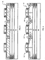
- FIG. 3 therein is shown a cross-sectional view of a monolithic VCSEL array 60 of the present invention in one stage of manufacturing.
- the array 60 includes a substrate 62.
- a lower mirror or lower DBR 64 which consists of a plurality of alternating high and low index of refraction materials.
- the lower DBR 64 can be made from a number of different combinations of dielectric layers, such as SiO 2 , SiC, TiO 2 , and Al 2 O 3 , they can be semiconductor layers, or they could be combinations of semiconductors, dielectric materials, and metal.
- Each of the layers is ⁇ 1/4 of a wavelength ( /4) in optical thickness and the layers are combined until the lower DBR 64 has an overall reflectance of almost 100%.
- the lower DBR 64 is a photoactive semiconductor structure 66, which contains quantum wells as previously described.
- the quantum well may be a single quantum well or multiple quantum wells with a number of alternating thin layers of high- and low-bandgap semiconductor materials.
- the photoactive semiconductor structure 66 is made from multiple layers of materials such as those containing aluminum, indium, gallium, arsenic, nitrogen, and/or phosphorous.
- the photoactive semiconductor structure 66 is a sacrificial layer, which has been formed into sacrificial islands 70 - 72 using standard lithography and etching processes.
- the sacrificial islands 70 - 72 can have different shapes, but in one mode, they are disk-shaped and have different diameters to allow control of the optical characteristics of the final VCODs as will later be explained.
- the sacrificial islands 70 - 72 are deposited on the photoactive semiconductor structure 66 and are of an etchable material, such as polyimide, which can readily be removed in an oxygen plasma. Alternately, they can be made of semiconductor layers that can be removed by selective etching.
- a reflector support 74 is deposited on the photoactive semiconductor structure 66 and covers the sacrificial islands 70 - 72.
- the reflector support 74 can be made of a material such as silicon nitride, an organic polymer, or it can be a semiconductor material.
- An anchor 76 is deposited on the reflector support 74 where it is attached to the photoactive semiconductor structure 66.
- the anchor 76 can be made with the same materials as the top DBRs 80-82, it can be made of dielectrics such as SiO 2 or Si 3 N 4 , or it can be a metal such as gold or aluminum.
- the materials used to form the upper DBRs 80-82 are deposited to cover the reflector support 74 and the anchor 76. These layers are alternating layers of low and high index of refraction materials that will be etched to form the upper mirrors or upper DBRs 80-82.
- the DBRs 80-82 can be made from dielectric materials such as SiO 2 , SiC, TiO 2 , and Al 2 O 3 . or they can be semiconductor layers, or they could be combinations of semiconductors, dielectric materials, and metal. There are a number of ways to deposit these materials such as plasma deposition, evaporation, sputtering, ion assisted deposition, or epitaxial growth.
- the upper DBRs 80 - 82 can have different shapes and sizes, but in the one preferred mode, they are disks having the same diameters centrally placed on portions of the reflector support 74 having different diameters.
- the upper DBR materials and the materials used for the reflector support 74 will contain residual stresses, either tensile or compressive.
- the existence of the residual stresses in these layers is evident to those having ordinary skill in the art.
- the stresses can be tailored in a variety of ways during the deposition of the films. In plasma deposition, various factors such as gas flows, temperature, and pressure can be changed to affect the internal stress in the deposited material. In sputtering, for example, the temperature and the voltage of the sputtering, or in ion-assisted deposition, the ion energy, affect the stress. The importance of these residual stresses will become apparent to those skilled in the art from the following descriptions.
- FIG. 4 therein is shown the cross-sectional view of the VCSEL array of FIG. 3 in one embodiment of the present invention.
- the same elements in FIG. 4 have the same numbers as in FIG. 3.
- the reflector support 74 which in one mode forms a plurality of different size drum-shaped configurations based on the disk-shape of the sacrificial islands 70 - 72, have been etched to form openings, such as sectors or holes, for removal of the sacrificial islands 70 - 72 by etching to create air gaps 84 - 86.
- openings such as sectors or holes
- the bows 87 - 89 in the reflector support 74 results in the air gaps 84 - 86 having different heights H1, H2, H3 at their centers due to the different diameters of the drum-shaped configurations.
- the heights H1, H2, H3 of the air gaps 84 - 86, respectively, and the thicknesses of the photoactive semiconductor structure 66 and the reflector support 74 define the optical heights of the resonant cavities of a plurality of VCODs 90 - 92 and, thus, the wavelengths of laser light they will emit when activated.
- the different heights H1, H2, H3 can be obtained through photolithography using a single mask to control the geometrical size and/or shape of the anchors or of the upper DBRs 80 - 82, or the geometrical size, shape, and/or configuration of the openings in the reflector support 74.
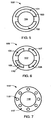
- FIG. 5 therein is shown a plan view of one embodiment of a single portion of a reflector support 100 according to the present invention.
- the reflector support 100 has two sector portions 101 and 102 removed to leave a single strap 103 supporting a reflector 104.
- FIG. 6 therein is shown a plan view of another embodiment of a single portion of a reflector support 105 according to the present invention.
- the reflector support 105 has four sectors 106 - 109 removed so a double strap 110 supports a reflector 112.
- FIG. 7 therein is shown a plan view of a further embodiment of a single portion of a reflector support 114 according to the present invention.
- the reflector support 114 has a plurality of openings 116 provided therein with the remaining portion 117 supporting a reflector 118.
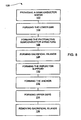
- a first step 122 is providing the wafer 52.
- a second step 124 is forming the lower DBR 64 over the wafer 52.
- a third step 126 is forming the photoactive semiconductor structure 66 over the lower DBR 64.
- a fourth step 128 is forming first and second sacrificial islands 70 and 71 of a sacrificial layer over the photoactive semiconductor structure 66 with the first and second sacrificial islands 70 and 71 having respective first and second different sizes. If the first and second sacrificial islands 70 and 71 are disk-shaped, the first and second sacrificial islands 70 and 71 will have first and second diameters, which are different. Different size and shape sacrificial islands can be formed for the entire wafer 52 using a single mask.
- a fifth step 130 involves forming the reflector support 74 over the first and second sacrificial islands 70 and 71.
- the reflector support 74 is conformally deposited over the first and second sacrificial islands 70 and 71 and is attached to the photoactive semiconductor structure 66 around the first and second sacrificial islands 70 and 71. It will be noted that the first and second sacrificial islands 70 and 71 are far enough apart that there is space between the first and second sacrificial islands 70 and 71 even after the reflector support 74 has been deposited.
- the sixth step 132 involves forming the anchor 76 between the first and second sacrificial islands 70 and 71 over the reflector support 74. Different sizes and shapes for the anchor 74 over the reflector support 74 can be formed for the entire wafer 52 using a single mask
- A. seventh step 134 involves forming first and second upper DBRs 80 and 81 over the reflector support 74. This involves depositing a reflector layer and patterning and etching the reflector layer to form the first and second upper DBRs 80 and 81. Different size and shape upper DBRs can be formed for the entire wafer 52 using a single mask.
- An eighth step 136 involves removing the first and second sacrificial islands 70 and 71 to form first and second air gaps 84 and 85.
- This step sectors or openings are formed in the reflector support 74 and the first and second sacrificial islands 70 and 71 are etched away through the openings to form the first and second air gaps 84 and 85.
- This removal step causes the first optical device 54 to be formed by the lower DBR 64, the photoactive semiconductor structure 66, the first air gap 84, and the first upper DBR 80.
- a second optical device 55 is formed by the lower DBR 64, the photoactive semiconductor structure 66, the second air gap 85, and the second upper DBR 81.
- the first and second air gaps 84 and 85 will be of different heights H1 and H2 due to: the stress imposed during the forming of the upper reflective layer; the geometrical size of the anchors 76 or of the first and second upper DBRs 80 and 81; or the geometrical size and configuration of the openings in the reflector support 74.
- the different heights H1 and H2 provide the first and second optical devices 54 and 55 with different emission wavelengths.
- the flow chart 120 is merely exemplary and many other steps may be added and some removed as would be evident to those having ordinary skill in the art.
- the wafer 52 can be sliced and packaged.
Landscapes
- Physics & Mathematics (AREA)
- Condensed Matter Physics & Semiconductors (AREA)
- General Physics & Mathematics (AREA)
- Electromagnetism (AREA)
- Optics & Photonics (AREA)
- Semiconductor Lasers (AREA)
Applications Claiming Priority (2)
| Application Number | Priority Date | Filing Date | Title |
|---|---|---|---|
| US151646 | 1993-11-15 | ||
| US10/151,646 US6806110B2 (en) | 2002-05-16 | 2002-05-16 | Monolithic multi-wavelength vertical-cavity surface emitting laser array and method of manufacture therefor |
Publications (2)
| Publication Number | Publication Date |
|---|---|
| EP1363369A1 EP1363369A1 (en) | 2003-11-19 |
| EP1363369B1 true EP1363369B1 (en) | 2006-05-03 |
Family
ID=29269815
Family Applications (1)
| Application Number | Title | Priority Date | Filing Date |
|---|---|---|---|
| EP03002337A Expired - Lifetime EP1363369B1 (en) | 2002-05-16 | 2003-02-03 | Monolithic multi-wavelength vertical-cavity surface emitting laser array and method of manufacture therefor |
Country Status (4)
| Country | Link |
|---|---|
| US (1) | US6806110B2 (enExample) |
| EP (1) | EP1363369B1 (enExample) |
| JP (1) | JP2003332686A (enExample) |
| DE (1) | DE60304931T2 (enExample) |
Cited By (1)
| Publication number | Priority date | Publication date | Assignee | Title |
|---|---|---|---|---|
| CN107565380A (zh) * | 2017-08-29 | 2018-01-09 | 中国航空工业集团公司洛阳电光设备研究所 | 一种共轴输出的多波长激光装置 |
Families Citing this family (36)
| Publication number | Priority date | Publication date | Assignee | Title |
|---|---|---|---|---|
| US7297471B1 (en) | 2003-04-15 | 2007-11-20 | Idc, Llc | Method for manufacturing an array of interferometric modulators |
| US7550794B2 (en) | 2002-09-20 | 2009-06-23 | Idc, Llc | Micromechanical systems device comprising a displaceable electrode and a charge-trapping layer |
| US7781850B2 (en) | 2002-09-20 | 2010-08-24 | Qualcomm Mems Technologies, Inc. | Controlling electromechanical behavior of structures within a microelectromechanical systems device |
| US7039075B2 (en) * | 2003-04-11 | 2006-05-02 | Thornton Robert L | Fiber extended, semiconductor laser |
| TW570896B (en) | 2003-05-26 | 2004-01-11 | Prime View Int Co Ltd | A method for fabricating an interference display cell |
| US7221495B2 (en) | 2003-06-24 | 2007-05-22 | Idc Llc | Thin film precursor stack for MEMS manufacturing |
| KR101354520B1 (ko) | 2004-07-29 | 2014-01-21 | 퀄컴 엠이엠에스 테크놀로지스, 인크. | 간섭 변조기의 미소기전 동작을 위한 시스템 및 방법 |
| DE102004052686A1 (de) * | 2004-08-23 | 2006-03-02 | Osram Opto Semiconductors Gmbh | Halbleiterbauelement mit einem gekrümmten Spiegel und Verfahren zum Herstellen eines Halbleiterbauelements mit einem gekrümmten Halbleiterkörper |
| US7492502B2 (en) | 2004-09-27 | 2009-02-17 | Idc, Llc | Method of fabricating a free-standing microstructure |
| TW200628877A (en) * | 2005-02-04 | 2006-08-16 | Prime View Int Co Ltd | Method of manufacturing optical interference type color display |
| US7831520B2 (en) * | 2005-06-28 | 2010-11-09 | Ebay Inc. | Mobile device communication system |
| CN101228091A (zh) | 2005-07-22 | 2008-07-23 | 高通股份有限公司 | 用于mems装置的支撑结构及其方法 |
| EP2495212A3 (en) | 2005-07-22 | 2012-10-31 | QUALCOMM MEMS Technologies, Inc. | Mems devices having support structures and methods of fabricating the same |
| JP2009503564A (ja) | 2005-07-22 | 2009-01-29 | クアルコム,インコーポレイテッド | Memsデバイスのための支持構造、およびその方法 |
| US7795061B2 (en) | 2005-12-29 | 2010-09-14 | Qualcomm Mems Technologies, Inc. | Method of creating MEMS device cavities by a non-etching process |
| US7382515B2 (en) | 2006-01-18 | 2008-06-03 | Qualcomm Mems Technologies, Inc. | Silicon-rich silicon nitrides as etch stops in MEMS manufacture |
| US7547568B2 (en) | 2006-02-22 | 2009-06-16 | Qualcomm Mems Technologies, Inc. | Electrical conditioning of MEMS device and insulating layer thereof |
| US7450295B2 (en) | 2006-03-02 | 2008-11-11 | Qualcomm Mems Technologies, Inc. | Methods for producing MEMS with protective coatings using multi-component sacrificial layers |
| US7527996B2 (en) | 2006-04-19 | 2009-05-05 | Qualcomm Mems Technologies, Inc. | Non-planar surface structures and process for microelectromechanical systems |
| US7623287B2 (en) | 2006-04-19 | 2009-11-24 | Qualcomm Mems Technologies, Inc. | Non-planar surface structures and process for microelectromechanical systems |
| US7321457B2 (en) | 2006-06-01 | 2008-01-22 | Qualcomm Incorporated | Process and structure for fabrication of MEMS device having isolated edge posts |
| US7763546B2 (en) | 2006-08-02 | 2010-07-27 | Qualcomm Mems Technologies, Inc. | Methods for reducing surface charges during the manufacture of microelectromechanical systems devices |
| US7733552B2 (en) | 2007-03-21 | 2010-06-08 | Qualcomm Mems Technologies, Inc | MEMS cavity-coating layers and methods |
| US7719752B2 (en) | 2007-05-11 | 2010-05-18 | Qualcomm Mems Technologies, Inc. | MEMS structures, methods of fabricating MEMS components on separate substrates and assembly of same |
| US7569488B2 (en) | 2007-06-22 | 2009-08-04 | Qualcomm Mems Technologies, Inc. | Methods of making a MEMS device by monitoring a process parameter |
| JP2009272375A (ja) * | 2008-05-01 | 2009-11-19 | Sumitomo Electric Ind Ltd | 半導体レーザの製造方法及び半導体レーザ |
| US7851239B2 (en) | 2008-06-05 | 2010-12-14 | Qualcomm Mems Technologies, Inc. | Low temperature amorphous silicon sacrificial layer for controlled adhesion in MEMS devices |
| US7864403B2 (en) | 2009-03-27 | 2011-01-04 | Qualcomm Mems Technologies, Inc. | Post-release adjustment of interferometric modulator reflectivity |
| CN102714396B (zh) * | 2010-01-29 | 2014-12-10 | 惠普发展公司,有限责任合伙企业 | 多模垂直腔表面发射激光器阵列 |
| US8659816B2 (en) | 2011-04-25 | 2014-02-25 | Qualcomm Mems Technologies, Inc. | Mechanical layer and methods of making the same |
| US9124062B2 (en) * | 2012-03-22 | 2015-09-01 | Palo Alto Research Center Incorporated | Optically pumped surface emitting lasers incorporating high reflectivity/bandwidth limited reflector |
| US9112331B2 (en) | 2012-03-22 | 2015-08-18 | Palo Alto Research Center Incorporated | Surface emitting laser incorporating third reflector |
| US9112332B2 (en) | 2012-06-14 | 2015-08-18 | Palo Alto Research Center Incorporated | Electron beam pumped vertical cavity surface emitting laser |
| JP5969677B2 (ja) * | 2015-10-05 | 2016-08-17 | ヒューレット−パッカード デベロップメント カンパニー エル.ピー.Hewlett‐Packard Development Company, L.P. | マルチモードのモノリシック垂直共振器面発光レーザアレイ及びこれを用いたレーザシステム |
| EP4071946A4 (en) * | 2020-01-08 | 2023-02-08 | Sony Group Corporation | ELECTROLUMINESCENT ELEMENT |
| JP2024110811A (ja) * | 2023-02-03 | 2024-08-16 | キヤノン株式会社 | アンテナ |
Family Cites Families (9)
| Publication number | Priority date | Publication date | Assignee | Title |
|---|---|---|---|---|
| US5291502A (en) | 1992-09-04 | 1994-03-01 | The Board Of Trustees Of The Leland Stanford, Jr. University | Electrostatically tunable optical device and optical interconnect for processors |
| US5739945A (en) | 1995-09-29 | 1998-04-14 | Tayebati; Parviz | Electrically tunable optical filter utilizing a deformable multi-layer mirror |
| US6324192B1 (en) * | 1995-09-29 | 2001-11-27 | Coretek, Inc. | Electrically tunable fabry-perot structure utilizing a deformable multi-layer mirror and method of making the same |
| JP2002500446A (ja) | 1997-12-29 | 2002-01-08 | コアテック・インコーポレーテッド | マイクロエレクトロメカニカル的に同調可能な共焦型の垂直キャビティ表面放出レーザ及びファブリー・ペローフィルタ |
| US5991326A (en) * | 1998-04-14 | 1999-11-23 | Bandwidth9, Inc. | Lattice-relaxed verticle optical cavities |
| US6341137B1 (en) | 1999-04-27 | 2002-01-22 | Gore Enterprise Holdings, Inc. | Wavelength division multiplexed array of long-wavelength vertical cavity lasers |
| US6675134B2 (en) * | 2001-03-15 | 2004-01-06 | Cerebrus Solutions Ltd. | Performance assessment of data classifiers |
| US6542531B2 (en) * | 2001-03-15 | 2003-04-01 | Ecole Polytechnique Federale De Lausanne | Vertical cavity surface emitting laser and a method of fabrication thereof |
| US6782019B2 (en) * | 2001-08-16 | 2004-08-24 | Applied Optoelectronics, Inc. | VCSEL with heat-spreading layer |
-
2002
- 2002-05-16 US US10/151,646 patent/US6806110B2/en not_active Expired - Fee Related
-
2003
- 2003-02-03 EP EP03002337A patent/EP1363369B1/en not_active Expired - Lifetime
- 2003-02-03 DE DE60304931T patent/DE60304931T2/de not_active Expired - Fee Related
- 2003-05-01 JP JP2003126147A patent/JP2003332686A/ja not_active Withdrawn
Cited By (2)
| Publication number | Priority date | Publication date | Assignee | Title |
|---|---|---|---|---|
| CN107565380A (zh) * | 2017-08-29 | 2018-01-09 | 中国航空工业集团公司洛阳电光设备研究所 | 一种共轴输出的多波长激光装置 |
| CN107565380B (zh) * | 2017-08-29 | 2019-04-16 | 中国航空工业集团公司洛阳电光设备研究所 | 一种共轴输出的多波长激光装置 |
Also Published As
| Publication number | Publication date |
|---|---|
| DE60304931D1 (de) | 2006-06-08 |
| EP1363369A1 (en) | 2003-11-19 |
| US20030214992A1 (en) | 2003-11-20 |
| JP2003332686A (ja) | 2003-11-21 |
| DE60304931T2 (de) | 2007-01-04 |
| US6806110B2 (en) | 2004-10-19 |
Similar Documents
| Publication | Publication Date | Title |
|---|---|---|
| EP1363369B1 (en) | Monolithic multi-wavelength vertical-cavity surface emitting laser array and method of manufacture therefor | |
| US6117699A (en) | Monolithic multiple wavelength VCSEL array | |
| EP1363370B1 (en) | Fixed wavelength vertical cavity optical devices and method of manufacture thereof | |
| US6744805B2 (en) | Single mode operation of microelectromechanically tunable, half-symmetric, vertical cavity surface emitting lasers | |
| EP1030420B1 (en) | A vertical cavity surface emitting laser array and a process for making same | |
| EP1182758B1 (en) | Multi-wavelength surface emitting laser and method for manufacturing the same | |
| AU2784799A (en) | Vertical optical cavities produced with selective area epitaxy | |
| US20020048301A1 (en) | Single mode operation of microelectromechanically tunable, half-symmetric, vertical cavity surface emitting lasers | |
| US6696307B2 (en) | Patterned phase shift layers for wavelength-selectable vertical cavity surface-emitting laser (VCSEL) arrays | |
| WO2000065700A2 (en) | Postgrowth adjustment of cavity spectrum for semiconductor lasers and detectors | |
| JP4360806B2 (ja) | 光学的にポンピングされる面発光型半導体レーザ装置および該装置の製造方法 | |
| US6693934B2 (en) | Wavelength division multiplexed vertical cavity surface emitting laser array | |
| KR20040010719A (ko) | 유전체 미러와 자기정렬 게인가이드를 구비한vcsel의 제조방법 및 장치 | |
| US6628685B1 (en) | Method of fabricating long-wavelength VCSEL and apparatus | |
| US6724796B2 (en) | Modified distributed bragg reflector (DBR) for vertical cavity surface-emitting laser (VCSEL) resonant wavelength tuning sensitivity control | |
| EP3435499B1 (en) | Method for making a semiconductor laser diode, and laser diode | |
| EP2033281B1 (en) | A method for fabricating a photonic crystal or photonic bandgap vertical-cavity surface-emitting laser | |
| US7116483B2 (en) | Distributed bragg reflector and method of fabrication | |
| US6061485A (en) | Method for wavelength division multiplexing utilizing donut mode vertical cavity surface emitting lasers | |
| WO2002089276A1 (en) | Surface emitting laser | |
| KR100460839B1 (ko) | 다채널 장파장 수직공진 표면방출 레이저 어레이 및 그제조방법 | |
| JP3944677B2 (ja) | 面発光型半導体レーザの製造方法 | |
| LAYER | F| G 1 AlGaAs |
Legal Events
| Date | Code | Title | Description |
|---|---|---|---|
| PUAI | Public reference made under article 153(3) epc to a published international application that has entered the european phase |
Free format text: ORIGINAL CODE: 0009012 |
|
| AK | Designated contracting states |
Kind code of ref document: A1 Designated state(s): AT BE BG CH CY CZ DE DK EE ES FI FR GB GR HU IE IT LI LU MC NL PT SE SI SK TR |
|
| AX | Request for extension of the european patent |
Extension state: AL LT LV MK RO |
|
| 17P | Request for examination filed |
Effective date: 20040420 |
|
| AKX | Designation fees paid |
Designated state(s): DE FR GB |
|
| GRAP | Despatch of communication of intention to grant a patent |
Free format text: ORIGINAL CODE: EPIDOSNIGR1 |
|
| GRAS | Grant fee paid |
Free format text: ORIGINAL CODE: EPIDOSNIGR3 |
|
| GRAA | (expected) grant |
Free format text: ORIGINAL CODE: 0009210 |
|
| AK | Designated contracting states |
Kind code of ref document: B1 Designated state(s): DE FR GB |
|
| REG | Reference to a national code |
Ref country code: GB Ref legal event code: FG4D |
|
| REF | Corresponds to: |
Ref document number: 60304931 Country of ref document: DE Date of ref document: 20060608 Kind code of ref document: P |
|
| REG | Reference to a national code |
Ref country code: GB Ref legal event code: 732E |
|
| ET | Fr: translation filed | ||
| RAP2 | Party data changed (patent owner data changed or rights of a patent transferred) |
Owner name: AVAGO TECHNOLOGIES FIBER IP (SINGAPORE) PTE. LTD. |
|
| PGFP | Annual fee paid to national office [announced via postgrant information from national office to epo] |
Ref country code: GB Payment date: 20070223 Year of fee payment: 5 |
|
| PLBE | No opposition filed within time limit |
Free format text: ORIGINAL CODE: 0009261 |
|
| STAA | Information on the status of an ep patent application or granted ep patent |
Free format text: STATUS: NO OPPOSITION FILED WITHIN TIME LIMIT |
|
| PGFP | Annual fee paid to national office [announced via postgrant information from national office to epo] |
Ref country code: DE Payment date: 20070330 Year of fee payment: 5 |
|
| 26N | No opposition filed |
Effective date: 20070206 |
|
| PGFP | Annual fee paid to national office [announced via postgrant information from national office to epo] |
Ref country code: FR Payment date: 20070221 Year of fee payment: 5 |
|
| GBPC | Gb: european patent ceased through non-payment of renewal fee |
Effective date: 20080203 |
|
| REG | Reference to a national code |
Ref country code: FR Ref legal event code: ST Effective date: 20081031 |
|
| PG25 | Lapsed in a contracting state [announced via postgrant information from national office to epo] |
Ref country code: DE Free format text: LAPSE BECAUSE OF NON-PAYMENT OF DUE FEES Effective date: 20080902 |
|
| PG25 | Lapsed in a contracting state [announced via postgrant information from national office to epo] |
Ref country code: FR Free format text: LAPSE BECAUSE OF NON-PAYMENT OF DUE FEES Effective date: 20080229 |
|
| PG25 | Lapsed in a contracting state [announced via postgrant information from national office to epo] |
Ref country code: GB Free format text: LAPSE BECAUSE OF NON-PAYMENT OF DUE FEES Effective date: 20080203 |